

Journal list menu

 Issue
IssueProgress in Photovoltaics: Research and Applications: Volume 27, Issue 12
i, 1059-1130December 2019
Export Citations
Download PDFs
COVER IMAGE
Cover Image
- Page: i
- First Published: 22 November 2019
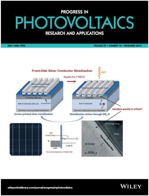
The cover image is based on the Research Article Tellurium-based screen-printable conductor metallizations for crystalline silicon solar cells by Kurt R. Mikeska et al., https://doi.org/10.1002/pip.3185. Cover image ©Jiangxi Jiayin Science and Technology Ltd. Images
ISSUE INFORMATION
RESEARCH ARTICLES
Potential of very thin and high-efficiency silicon heterojunction solar cells
- Pages: 1061-1070
- First Published: 08 August 2019

The potential of very thin c-Si solar cells is examined by fabricating and characterizing silicon heterojunction solar cells with a thickness range from 40 to 400 μm. The impact of the wafer thickness on photovoltaic parameters is evaluated and analyzed with simulation. A high efficiency of 22% is achieved using a very thin wafer (46 μm), demonstrating a high potential for flexible high-efficiency c-Si solar cells.
Tellurium-based screen-printable conductor metallizations for crystalline silicon solar cells
- Pages: 1071-1080
- First Published: 30 August 2019
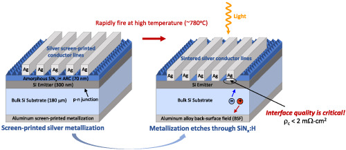
Tellurium-based screen-printable metallization pastes containing multiple inorganic solid-state frits (pastes containing two or more discrete tellurium-based frits) were prepared with varying ratios of tellurium and lead cations and evaluated on c-Si PERC wafers. Cells fabricated from pastes containing multiple frits had state-of-the-art electrical properties (Eff = 21.1%). Multiple frit systems allow for the fine-tuning of the final metallization chemistry to further improve solar cell performance, which is essential for advanced c-Si devices and continued reductions in processing costs.
Plasma-immersion ion implantation: A path to lower the annealing temperature of implanted boron emitters and simplify PERT solar cell processing
- Pages: 1081-1091
- First Published: 19 August 2019
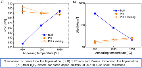
We report a new way to activate implanted boron emitter at low temperature that is the use of plasma-immersion ion implantation(PIII) from B2H6 plasma. A full activation of the emitter at 950°C was observed even for a high implantation dose corresponding to a sheet resistance of 112 Ω/sq. Promising performances while being integrated in n-PERT solar cells fully doped by PIII were demonstrated with efficiency of 20.8%.
Modified laser-fired contact process for efficient PERC solar cells
- Pages: 1092-1103
- First Published: 30 August 2019
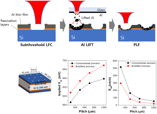
We developed a modified LFC process by combining conventional LFC and LIFT technologies to reduce laser damage and enhance local BSF at the local contact holes while maintaining low contact resistances. The modified LFC process comprises three steps: (a) subthreshold LFC step, (b) LIFT step, and(c) PLF step, providing enhanced implied Voc and lower contact resistances in comparison with a conventional LFC process.
Tunnel oxide passivating electron contacts for high-efficiency n-type silicon solar cells with amorphous silicon passivating hole contacts
- Pages: 1104-1114
- First Published: 16 October 2019
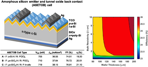
High-efficiency hybrid silicon solar cell was achieved by combining twopassivating contact structures, a heterojunction and a polysilicon passivating contact. The efficiency of 21.8% was achieved and the simulation showed that the efficiency can be reached to 26%.
Influences of buffer material and fabrication atmosphere on the electrical properties of CdTe solar cells
- Pages: 1115-1123
- First Published: 11 September 2019
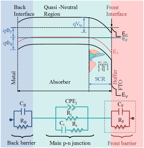
A three-subcircuit model with explicit representation of the front contact barrier is developed to measure the front and back contact barrier heights as well as energy levels and densities of defects at interface and in absorber of CdTe thin-film solar cells using impedance spectroscopy.
LITERATURE SURVEY
PHOTOVOLTAICS LITERATURE SURVEY (No. 154)
- Pages: 1125-1130
- First Published: 22 November 2019