Optical Nanolinks With Yagi–Uda-Loop and Dipole Antennas Fed by Gaussian Beam
Abstract
This work presents a theoretical comparative analysis of wireless optical nanolinks with different cylindrical plasmonic nanoantennas fed by a Gaussian beam. The nanolinks considered are Yagi–Uda-loop/dipole, Yagi–Uda/dipole and dipole/dipole, where the operating wavelength is λ = 1153 nm. The numerical analysis of these nanolinks was performed by the linear moment method with an equivalent surface impedance of the conductors. With this method, the following parameters were evaluated by each nanlolink: current along the antennas, near field distributions and the power transmission in the receiving antenna. The results show that the Yagi–Uda-loop/dipole nanolink presents an improvement of approximately 5 dB in relation to the dipole/dipole nanolink and 3.2 dB in relation to the Yagi–Uda/dipole nanolink.
1. Introduction
In recent years, optical nanoantennas have been the subject of great interest in the scientific community thanks to their ability to amplify, manipulate, and confine optical fields beyond the diffraction limit of light [1]. Due to these characteristics, they offer unique opportunities for applications in more efficient photovoltaic devices [2], optical sensors [3, 4], optical circuits [5], fiber optics [6], and wireless optical nanolinks [7–11], which can be used, for example, to interconnect different devices in an integrated nanophotonic circuit.
Optical wireless communications have recently emerged as a promising alternative for chip-scale interconnects, particularly through the use of plasmonic nanoantennas that allow subwavelength field confinement and highly directional radiation. Among the proposed architectures, Yagi–Uda nanoantennas stand out as efficient optical analogs of traditional radio-frequency antennas, offering high directivity and front-to-back ratios [12]. In [12], Maksymov et al. provided a comprehensive review of the design and application of these antennas in the optical regime, emphasizing the necessity to adapt classical design strategies due to plasmonic resonance effects. Building on this foundation, Damasceno et al. [13] proposed a systematic optimization strategy for chip-scale Yagi–Uda nanoantennas, considering variations in the length and spacing of metallic elements. Furthermore, Damasceno et al. [14] introduced reconfigurable magnetoplasmonic nanoantennas whose emission direction can be controlled magnetically, enabling active and tunable links on integrated platforms. Another significant contribution came from Elsaid et al. [15], who proposed rhombic nanoantennas with broadband response and high efficiency at 1550 nm, making them attractive candidates for optical telecommunication systems. In addition, Solís et al. [16] demonstrated that matched directive nanoantennas significantly outperform omnidirectional structures and plasmonic waveguides by reducing absorption losses and improving coupling efficiency. Despite these advances, comparative studies involving different plasmonic nanoantenna topologies in wireless nanolinks excited by spatially confined optical beams, such as Gaussian beams, remain scarce, a gap this work aims to address.
This work presents a comparative analysis of nanolinks formed by transmitting and receiving cylindrical plasmonic nanoantennas, where the transmitting antennas are fed by a Gaussian beam, which is a more realistic power source, with a wavelength equal to λ = 1153 nm. The antennas used in the links are Yagi–Uda-loop, Yagi–Uda, and dipole, where the first consists of a Yagi–Uda antenna coupled to a cylindrical parasitic loop. These nanoantennas have already been analyzed in isolated situations, being fed by a voltage source. However, this work investigates these nanoantennas for the first time in wireless nanolinks and fed by a Gaussian beam.
Three nanolinks are analyzed: Yagi–Uda-loop/dipole, Yagi–Uda/dipole and dipole/dipole, where the dipole is the receiving antenna in all cases. The analysis of these electromagnetic problems was performed by the linear Method of Moments (MoMs), in the same way as was done in [17, 18]. The results show the current along the antennas and the near field distributions. Also, the relation between the power received by the load connected in the terminals of the receiving antenna and the Gaussian beam power is investigated as a function of the distance between transmitter and receiver. This relation we call here transmission power. Section 2 presents the theoretical development, Section 3 shows the numerical results, and Section 4 discusses the conclusions.
2. Theoretical Development
2.1. Geometries of the Nanolinks
Three models of nanolinks are investigated, each with different antenna configurations for transmission and reception: the first model consists of Yagi–Uda-loop/dipole antennas, with a Yagi–Uda-loop antenna for transmission and a dipole for reception (Figure 1(a)); the second model is composed of Yagi–Uda/dipole antennas, with a Yagi–Uda antenna for transmission and a dipole for reception (Figure 1(b)); and the third model employs dipole/dipole antennas, where both the transmitting and receiving antennas are of the dipole type (Figure 1(c)).
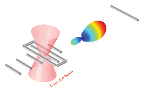
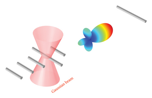
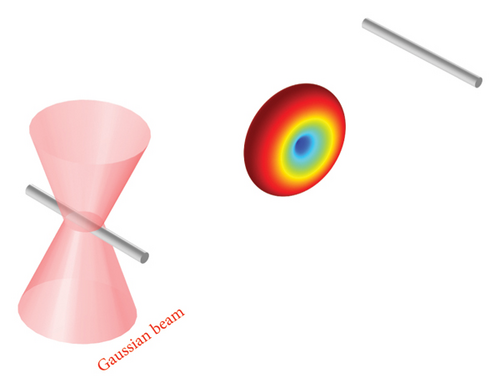
Figure 2(a) shows the geometry of the Yagi–Uda-loop/dipole nanolink. A Gaussian beam is used to feed the nanoantenna located on the left side (Yagi–Uda-loop antenna), which acts as the transmitter. This antenna converts the near field receiving from the Gaussian beam into optical radiation (scattered field), which propagates through free space. The nanoantenna positioned on the right serves as the receiver (dipole antenna), capturing the radiation emitted by the transmitting antenna and converting it into received power across the load ZC.
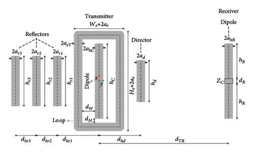
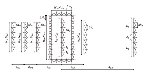
The antennas are made by cylindrical gold conductors positioned in free space. The transmitting nanoantenna is composed by one central dipole, one director, three reflectors, and a rectangular loop (Figure 2(a), left side). The central dipole is located in the z = 0 plane, along the x axis and centered at the origin, with length hC and radius ahC. The director has length hd and radius ad. The reflectors (first, second, and third) have lengths hr1, hr2, and hr3 and radii ar1, ar2, and ar3, respectively.
The rectangular loop has length He + 2ae, width We + 2ae, radius ae, and the parameters dW and dH are the distances between the surfaces of the dipole and the loop. The parameters dhd, dhr1, dhr2, and dhr3 are the distances between the elements of the Yagi–Uda antenna (Figure 2(a) left). The receiving antenna is a dipole (Figure 2(a) right), located in the plane z = 0 and displaced by a distance dTR with respect to the axis of the dipole of the transmitting antenna, of total length 2hR + dR, radius ahR, and size dR of the center gap where the load ZC is connected.
The geometry of the Yagi–Uda/dipole and dipole/dipole nanolinks is based on the Yagi–Uda-loop/dipole link model (Figure 2(a)), with simplifications. The geometry of the Yagi–Uda/dipole link is the same as the Yagi–Uda-Loop/dipole, but without the loop element. The geometry of the dipole/dipole link uses only simple dipoles in transmission and reception, removing the reflectors, the director, and the loop element.
2.2. MoMs Model
To analyze the nanolink configurations depicted in Figure 1, we employ the linear MoMs to solve the one-dimensional integral equation governing the electric field. The solution is obtained using a linear approximation of the longitudinal current, with sinusoidal basis functions and rectangular pulse testing functions, as described in [17].
The nanoantennas are modeled using gold as the conducting material, whose complex permittivity is described by the Lorentz–Drude model [19]. A detailed implementation of this model, including the specific parameters used for gold in the optical frequency range, can be found in [17].
2.3. Gaussian Beam
3. Numerical Results
In this section, we initially discuss the accuracy of the MoM code developed in MATLAB, based on the mathematical model presented in Section 2, by comparing a simulation example performed using the MoM and the Comsol Multiphysics software [22]. Subsequently, we analyze the proposed nanoantennas alone and later the wireless nanolinks. The numerical results for the isolated nanoantennas and wireless nanolinks are presented considering their excitation by a Gaussian beam with a wavelength of λ = 1153 nm.
3.1. Theoretical Validation of the MoM Model
To verify the theoretical accuracy of MoM, this section presents a simulation example, performed by MoM and the Comsol Multiphysics software [22], of a cylindrical gold nanorod located in free space, positioned along the x-axis and centered at the origin. The nanoantenna of length hC and radius ahC = 27 nm is illuminated by an ideal Gaussian beam (power source) polarized on the x-axis and propagating in the +z direction. The beam has radius w, beam waist w0, power P, and operating wavelength λ. The Gaussian beam model is shown in detail in chapter 9 of reference [21]. In this example, a fixed Gaussian beam was used, with power P = 10−12 W, wavelength λ = 1153 nm, and beam waist w0 = 340 nm.
Figure 3 shows the variation of the current amplitude at the center (IC) of the cylindrical nanobar as a function of the length hC and radius ahC = 27 nm, simulated by MoM and Comsol software. The figure shows good agreement between the two methods, which reflects excellent accuracy and convergence of MoM. The difference between the results occurs because MoM uses a 1D current element approximation for the cylindrical conductor, while Comsol uses 3D elements.
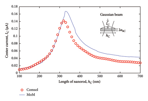
MoM discretizes only the conductor and Comsol discretizes the conductor and the domain around the conductor. Therefore, MoM uses a smaller number of elements, which results in computational gains in terms of memory and processing time.
Other comparisons of results between the MoM model and the Comsol software for cylindrical structures are found in [17, 18, 23, 24]. In [23], the structure is a dipole-loop nanoantenna fed by a two-wire optical transmission line; in [24], a dipole fed by a voltage source; in [18], an optical nanocircuit fed by a Gaussian beam; and in [17], are nanobar and nanodipole fed by a plane wave and optical nanocircuit fed by a voltage source.
3.2. Transmitting Antennas
In this section, the Yagi–Uda-loop, Yagi–Uda, and dipole antennas are analyzed separately. For this analysis, the antenna parameter values are those shown in Table 1, where with these values the main resonance is around 260 THz (λ ≈ 1153 nm). The parameters of the transmitting antennas are based on [25], where the author used the optimization method called adaptive fuzzy GAPSO, to find the best geometry for the nanoantennas.
| Dipole | 1streflector | ||||||
|---|---|---|---|---|---|---|---|
| Length (hC) | Radius (ahC) | Length (hr1) | Distance (dr1) | Radius (ar1) | |||
| 550 nm | 27 nm | 285 nm | 291 nm | 30 nm | |||
| Director | 2ndreflector | ||||||
| Length (hd) | Distance (dd) | Radius (ad) | Length (hr2) | Distance (dr2) | Radius (ar2) | ||
| 254 nm | 267 nm | 29 nm | 281 nm | 283 nm | 30 nm | ||
| Rectangular loop | 3ndreflector | ||||||
| dW | dH | Length (He) | Width (We) | Radius (ae) | Length (hr3) | Distance (dr3) | Radius (ar3) |
| 50 nm | 20 nm | 630 nm | 194 nm | 20 nm | 280 nm | 290 nm | 28 nm |
The excitation beam used to feed the transmitting antennas is focused on the transmitting dipole with polarization along the dipole axis (x-axis), the propagation direction is +z, the beam axis is along the z axis, and the minimum beam waist (w0) is located at z = 0, which is the plane of the nanoantennas. In all analyses a fixed Gaussian beam will be used, with power P = 10−12W, wavelength λ = 1153 nm, and beam waist w0 = 340 nm. The beam parameters are based on [18].
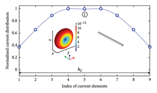
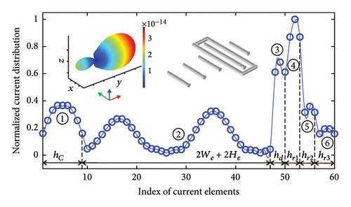
Figure 4 presents the results of current distribution and 3D far-field radiation (radiation intensity) diagram for the isolated nanodipole (Figure 4(a)), Yagi–Uda (Figure 4(b)), and Yagi–Uda-loop (Figure 4(c)). For the isolated nanodipole (Figure 4(a)), it is possible to observe the 3D diagram with the conventional omnidirectional radiation pattern of the dipole and the expected current distribution, presenting the half-wavelength λ/2 format.
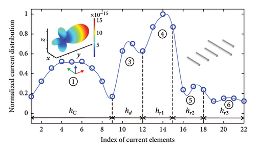
In the case of the isolated Yagi–Uda nanoantenna (Figure 4(b)), the directional radiation diagram is observed, with the main lobe (+y direction) and three small side lobes. In the current distribution, some limits are drawn to identify the current of each element of the Yagi–Uda nanoantenna, from left to right, they are dipole (hC), director (hd), reflector 1 (hr1), reflector 2 (hr2), and reflector 3 (hr3).
In the case of the Yagi–Uda-loop nanoantenna (Figure 4(c)), the directional radiation diagram is observed, with the main lobe (+y direction), and a small secondary lobe in the −y direction. In the current distribution, some limits are drawn to identify the current of each element of the Yagi–Uda-loop nanoantenna, from left to right, they are dipole (hC), loop (2We + 2He), director (hd), reflector 1 (hr1), reflector 2 (hr2), and reflector 3 (hr3). It can be observed that all elements of the Yagi–Uda-loop antenna have a dipolar current distribution pattern, approaching half a wavelength λ/2. In addition, the current amplitude is smaller in the reflectors furthest from the dipole.
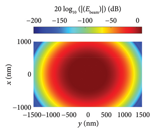
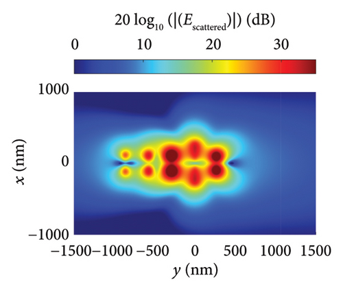
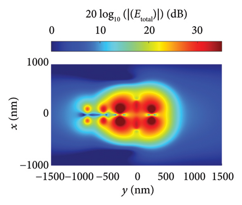
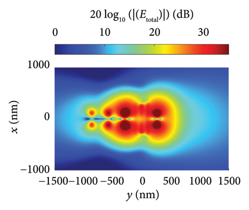
Figures 5(a), 5(b), and 5(c) illustrate the distribution of the incident, scattered, and total near fields, respectively, for the isolated nanodipole. Similarly, Figures 6(a), 6(b), and 6(c) present the distribution of the incident, scattered, and total near fields for the Yagi–Uda nanoantenna. Figures 7(a), 7(b), and 7(c) show the same field distributions for the Yagi–Uda-loop nanoantenna. It can be observed in Figures 5(b), 5(c), 6(b), 6(c), 7(b), and 7(c) that regions with higher electric field intensity are located near the nanoantennas, indicating strong coupling between the Gaussian beam and the transmitting nanoantennas. In other words, the Gaussian beam is effectively exciting these nanostructures.
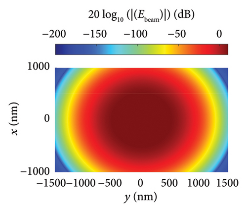
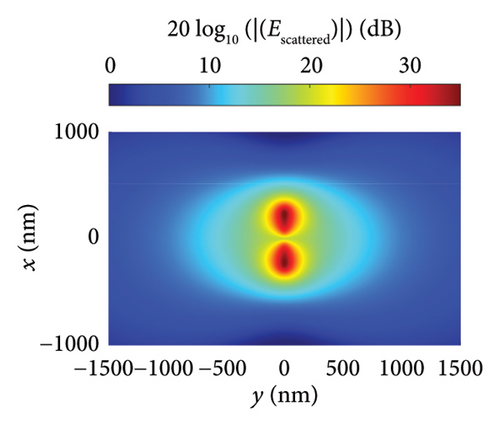
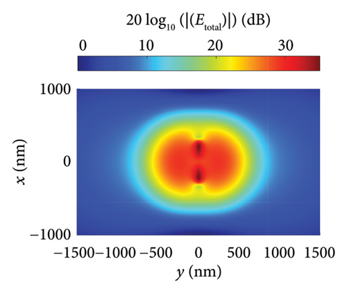
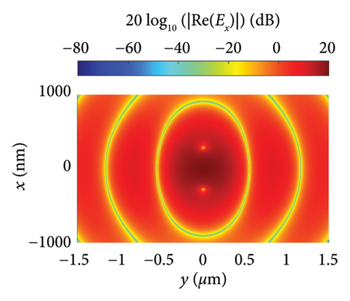


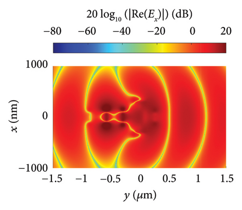
Figures 5(d), 6(d), and 7(d) show the magnitude and phase of the near-field electric field distribution, E = 20 log10 (|Re (Ex)|), for the dipole, Yagi–Uda, and Yagi–Uda-loop antennas, respectively, in the z = ahC + 20 nm plane. In this result, a more spherical wavefront is observed in Figure 7(d) mainly due to the loop, which has a more spherical geometry in this plane.
3.3. Wireless Optical Nanolinks
This section presents the results obtained in the analysis of the dipole/dipole nanolink (Figure 2(a), without director, reflectors, and loop), Yagi–Uda/dipole (Figure 2(a) without the loop), and Yagi–Uda-loop/dipole (Figure 2(a)). The parameters used for the transmitting antennas are the same as in the previous section and for the receiving antennas, the parameters used were hR = 260 nm, dR = 30 nm, and adR = 27 nm. For each nanolink, a load ZC = 50 Ω was used and connected to the terminals of the receiving dipole antenna.
The power transfer between transmitter–receiver links can be investigated by calculating the power transmission (or power transfer function). This parameter can be calculated approximately using the Friis analytical transmission equation [26], as was done in [7, 9, 10], or more precisely by the numerical model of MoM [8, 17, 23]. The definition of this parameter is the ratio between the power delivered to the load ZC and the power delivered to the transmitting antenna. In MoM, this power can be given by PZC/Pin = (0, 5) |IC| Re (ZC)/(10−12), where the Pin used was the power of the Gaussian beam (Pin = 10−12 W). The calculation of transmission power using the MoM model offers significant advantages over other methods, such as the finite difference time domain (FDTD) and the finite element method (FEM). In these methods, analyzing large distances would be computationally impractical, as it would require an enormous amount of memory to discretize the entire analysis domain. In contrast, the MoM overcomes this limitation by discretizing only the geometry of the antenna, significantly reducing computational demands [23].
Figure 8 shows the power transmission behavior, as a function of distance, for the dipole/dipole, Yagi–Uda/dipole, and Yagi–Uda-loop/dipole nanolinks. In addition, the figure also presents the power transmission characteristics of a bifilar cylindrical optical transmission line (OTL), which connects the transmitting and receiving nanoantennas shown in Figure 2(a), but without the inclusion of directors, reflectors, or the loop element, thus forming a basic optical nanocircuit. The transmitting nanoantenna is excited by the same Gaussian beam used in the wireless nanolinks. The OTL has a conductor radius of 15 nm and a total length of 5 μm.
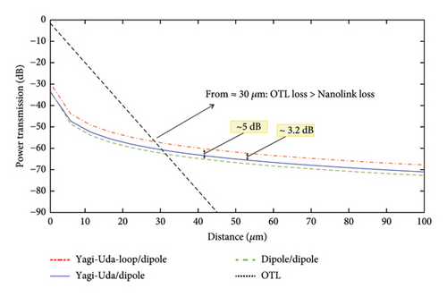
The losses in the OTL are estimated using the same methodology described in [18] and further supported by [27]. In this approach, the loss constant α, which remains approximately constant for the dominant propagation mode in the OTL, is determined by the average slope of the current amplitude in decibels (dB) as a function of distance along the transmission line. Mathematically, this is expressed as α = ΔI/ΔL, where ΔI represents the average current decay in dB over a distance ΔL. For the configuration analyzed, the estimated value of α was approximately 0.0019954 dB/nm for an OTL of length L = 5 μm.
Figure 8 shows that wireless optical nanolinks can have lower loss compared with wired nanolinks, from a certain distance, which for the considered cases is from 30 μm. This shows that optical nanolinks based on nanoantennas are more suitable than OTL for communication at distances above approximately 30 μm. In addition, the Yagi–Uda-loop/dipole nanolink presents an improvement of approximately 5 dB compared with the dipole/dipole nanolink and 3.2 dB compared with the Yagi–Uda/dipole nanolink. The Yagi–Uda/dipole nanolink presents an improvement of 1.7 dB compared with the dipole/dipole nanolink.
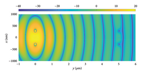
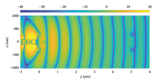
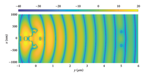
Figure 9 shows the near-field electric field distribution, E = 20 log10 (|Re (Ex)|), of the dipole/dipole (Figure 9(a)), Yagi–Uda/dipole (Figure 9(b)), and Yagi–Uda-loop/dipole (Figure 9(c)) nanolinks, in the z = ahC + 20 nm plane, for a distance between the transmitting and receiving antennas of 5 μm. In the three nanolinks shown in this figure, one can observe the electric field propagating from the transmitting antennas to the receiving antennas. Furthermore, the decay of the electric field intensity of the wave front with distance is observed. We observe that the case of Yagi–Uda-loop/dipole (Figure 9(c)) presents higher field intensities near de receiving antennas. This is in accordance with the best power transmission presented in Figure 8.
4. Conclusions
This work presented a comparative analysis of nanolinks formed by Yagi–Uda-loop, Yagi–Uda, and dipole plasmonic nanoantennas fed by Gaussian beam. The linear MoMs with equivalent surface impedance were used to model the scattering problems, where a simulation example was compared with finite element calculations and a good agreement was observed. The results obtained were the near field and current distributions for the three isolated antennas and three nanolinks and the transmission power of the proposed nanolinks. The results showed that the Yagi–Uda-loop/dipole case presents an improvement of approximately 5 dB in relation to the dipole/dipole case and 3.2 dB in relation to the Yagi–Uda/dipole case. Also, we proved that the wireless nanolinks analyzed present better transmission over distances larger than 30 μm, when compared with wired nanolinks of bifilar OTL type. This result is of great importance for future applications in wireless communication at the nanoscale. In future works, nanolinks with Yagi–Uda-loop in both transmitter and receiver can be used to improve the power transmission.
Conflicts of Interest
The authors declare no conflicts of interest.
Funding
This work was supported by Fundação Amazônia Paraense de Amparo à Pesquisa; Pró-Reitoria de Pesquisa e Pós-Graduação, Universidade Federal do Pará.
Acknowledgments
The authors would like to thank the Brazilian agencies Amazon Foundation for Studies and Research Support (FAPESPA) and the Pro-Rectory of Research and Postgraduate Studies of the Federal University of Pará (PROPESP/UFPA) for providing funding for this research work.
Open Research
Data Availability Statement
The data that support the findings of this study are available from the corresponding author upon reasonable request.


