Gain Improvement of Bidirectional Substrate-Integrated Waveguide-Based Circular Cavity-Backed Hexagonal Split Ring-Shaped Slotted Antenna Using Metamaterial as Superstrate
Abstract
A low profile substrate-integrated waveguide (SIW)-based circular cavity-backed slotted antenna is proposed at an operating frequency of 5.42 GHz for wireless applications in U-NII-2B band in the TM010 fundamental mode. Two hexagonal split ring-shaped slots of 7 and 4 mm radius are placed on the patch as well as on the ground plane, resulting in bidirectional radiation. The reflection coefficient (S11) and gain for the single split ring-shaped hexagonal slotted antenna (Antenna-I) resonating at a frequency of 5.52 GHz is obtained as −23.4 and 6 dBi, respectively, having impedance bandwidth of 5.48–5.57 GHz while −29.8 dB and 7.2 dBi values of reflection coefficient and gain are obtained for double split ring hexagonal-shaped slotted SIW cavity-backed antenna (Antenna-II) operating at 5.42 GHz. Furthermore, a band pass metamaterial operating in the frequency band of 5.19–5.57 GHz is used as a superstrate to augment the characteristics of the antenna and it is found that the gain is improved by 3.8 dBi as compared with Antenna-I and 2.6 dBi as compared with Antenna-II. The antenna–metamaterial composite structure is designed and fabricated on Arlon AD270 and Arlon AD320 substrate, respectively. Parametric studies are performed on the composite structure with respect to reflection coefficient, gain and metamaterial layer placement on the antenna to achieve the best results. Simulations are performed on HFSS v19.0 and show resemblance with the measured results.
1. Introduction
Substrate-integrated waveguides (SIWs) have been adopted as a widespread choice for microwave components and antennas due to their superior performance and power-handling capabilities. Unlike conventional waveguides, SIW structures offer consistent electrical shielding, making them ideal for various applications. Circular cavities and waveguides within SIW structures support multiple operational modes, providing flexibility in design. For cost-effective, low-profile antennas, cavity-backed [1, 2] designs are a popular option. These antennas are known for their high gain, unidirectional radiation patterns and ability to handle high power levels. SIW-based cavity-backed antennas provide the possibility of fabrication on a single substrate, offering advantages such as reduced cost, planar integration, and excellent radiation performance. Compared with traditional slot antennas, SIW-based slot antennas often exhibit lower front-to-back ratios and reduced mutual coupling, tailoring them for wireless communication applications [3–5]. The compact size and economic benefits of SIW-based cavity-backed antennas make them an attractive choice for integrating planar circuits. Various SIW structures such as oscillators, mixers, amplifiers, slotted waveguides and antenna types resembling leaky-wave and cavity-backed antenna structures have been mentioned in the existing literature [6, 7]. The versatility of SIW technology has contributed to its widespread adoption in microwave and antenna design. A triband Y-shaped slot antenna [8] operates at three frequencies of 5.7, 6 and 6.4 GHz, using three feed lines. It offers high isolation (over 24 dB) and gain (around 6 dBi) between ports. Gain enhancement for circular SIW cavity antennas can be achieved through various methods like multiple cavity-backed slot antennas [9], which demonstrates that using a single, two or 2 × 2 array on TLY031 material, composite feeding elements which combines SIW and coplanar waveguide [10] or SIW and microstrip lines [11] can enhance performance. Dual-band configurations presented in [12] can also be used to enhance the gain, where the design with nested circular and rectangular cavities and individual radiating slots are presented. In [13], a microstrip-to-SIW transition is proposed on a triangular slotted antenna which achieves 6 dBi gain over 20.2–21.1 GHz on FR4 substrate. A dual-band planar antenna with modified split ring resonator slots on the patch of the antenna is designed [14] with partial ground structure for GSM and WiMAX applications. Square-shaped split ring resonators are used to dual-band antenna operating at 900 MHz with reflection coefficient of 22.26 dB and 18.97 dB for 3.3 GHz. On the other hand, the authors in authors [15] have designed a fractal antenna with square SRR using the square Sierpinski fractal technique to obtain multiple resonating modes. The antenna resonates at a dual frequency for global system for mobile communication and sub−6 GHz 5G applications. Dual T-shaped slot with shorted via was used in the proposed design by Chaturvedi [16] to enhance the bandwidth while exciting the three higher modes, that is, TE110, TE120, and TE130 modes on a SIW cavity of size 0.86 λg × 0.86 λg mm2. Circular-shaped cavity resonator with squared slot was placed on the patch to excite the two modes, that is, slot mode and inset patch mode using probe feed to reduce the cross polarisation in antennas [17]. SIW cavity-backed slotted antenna with folded grounded coplanar waveguide feeding system was designed [18] to excite the cavity in three higher modes, resulting in enhanced bandwidth of 1.4 GHz. When the researchers in [19] have placed rectangular cavity on the ground surface, leading to TE210 mode excitation in even and odd modes, the slot shape is modified to ‘I’ resulting in enhancement of bandwidth by 17.2%. A mixture of hexagonal and rectangular slots enhances the bandwidth by 21.6% for applications in the X band frequency range [20]. It excites TE110 and TE120 modes for bandwidth enhancement.
Frequency selective surfaces (FSSs) have been extensively studied for over 6 decades due to their wide-ranging applications in communications. FSS layers are planar arrays of patches or dipoles, often fabricated on rigid substrates. They can act as passband or stopband filters based on their design. FSS have various uses, including Antenna reflectors that helps in improving gain [21], in radomes which provides dual-band bandpass transmission [22] and as shielding that controls electromagnetic wave transmission. Split ring-shaped resonators, patches, holes and crossed structures are some of the common FSS structures. The quality factor can be adjusted by controlling the element size and spacing [23]. Researchers are exploring the areas of fractal FSSs [24] and metamaterials [25]. Some of the examples of FSS applications reported in literature are discussed. Single-layer FSS finds its usage in a dual-band antenna operating at 2.4 and 5.8 GHz and enhances the gain to 7.54 and 6.8 dBi, respectively, as given in [26]. The gain enhancement and directivity can be achieved by placing the FSS as a superstrate given in [27–31]. Also, dual dielectric resonators [32] demonstrate gain enhancement by placing FSS over them. As discussed in [33], FSS can be used on a square-shaped DD patch antenna for operations in high frequency range while the high gain can be achieved by integrating FSS with HIS to achieve a value of 10.4 dBi gain as given in [34]. The authors in [35] have proposed a composite antenna–FSS that helps in gaining enhancement by using FSS as superstrate. Some of the self-triplexing SIW antennas and leaky antennas are discussed in [36–39]. Mondal et al. [40] proposed a partially reflecting hexagonal-shaped FSS as superstrate. It was found that the decoupled system resulted in better performance as compared with the coupled system.
The authors have proposed a SIW-based circular cavity-backed antenna with hexagonal shaped slots on both the metallic surfaces and it operates at 5.42 GHz frequency in U-NII-2B band for wireless communication. The hexagonal slot is initially placed on the ground surface and the antenna resonates at 5.52 GHz with a gain of 6 dBi. Furthermore, the design is modified with the intrusion of hexagonal slot on the patch and now, and the antenna resonates at 5.42 GHz having a gain of 7.1 dBi. Finally, when the FSS is placed over the proposed antenna structure and now, the antenna–FSS structure improves the gain to 9.8 dBi at 5.42 GHz. The proposed antenna is designed and fabricated using Arlon AD270 substrate while Arlon AD320 is used for fabrication of FSS layers. Simulation results generated from ANSYS HFSS v19.0 closely matched the measured results.
2. Materials and Methods
2.1. Antenna Composition
SIW-based circular shaped cavity-backed antenna with hexagonal shaped slots is proposed to function at a frequency of 5.42 GHz in the dominant mode.
The cavity design is altered by incorporating metallic vias on the circumference of the circular cavity, leading to the perfect electric conducting (PEC) walls. It is seen that the metallic vias of diameter (s) = 1 mm and centre-to-centre distance (p) of 1.5 mm are drilled in such a way that they connect the upper and lower metallic surfaces fulfiling the mandatory conditions of s < λg/5 and p < 2s [6], where λg is the guided wavelength, s is the via diameter and p is the centre-to-centre distance between vias to prevent leakage of waves. This structure of metallic vias with cavity results in a structure that resembles to SIW. The trapped electromagnetic waves due to the vias are released using the slots. In this case, two hexagonal slots are used in such a way that one slot is placed on the above metallic surface (patch) and another slot is placed on the bottom surface (ground). The hexagonal-shaped slots offer better magnetic coupling and uniform current distribution. Hence, the hexagonal-shaped slots are chosen to design the proposed antenna.
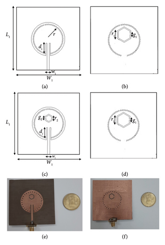
The proposed antenna consisting of a circular patch (r = 16 mm, ϵr = 2.7 and h = 0.79 mm) on Arlon AD270 substrate is described in this paper, having a dimensions of 1.1 λ0 × 1.1 λ0 × 0.01 λ0. Since Arlon provides the advantage of low insertion loss and low tangent loss, it is used to design the proposed antenna. Due to the presence of PEC wall, the radius extending till the metallic vias is 13.4 mm, where 16 −(1.6 + 1) = 13.4 mm, as depicted in Figure 1(a) with its fabricated prototype. A hexagonal split ring shaped slot of radius = 7 mm, width of strip = 0.8 mm and split gap between two rings = 1 mm is initially placed on the ground plane as shown in Figure 1(b) to release the electric and magnetic energies from the enclosed cavity. The SIW circular cavity finds its application as frequency stabiliser element in feedback loop. The depth of inset feed di = 11.85 mm and width wi = 2.13 mm is placed at the centre line to excite the cavity in the fundamental mode, that is, TM010 mode. The proposed antenna emits in the backward direction due to the insertion of slot on the ground surface. Another hexagonal slot is placed on the above surface as shown in Figure 1(c). Proposed antenna dimensions with hexagonal slots are given in Table 1.
| L1 | W1 | r | di | wi | g1 | g2 | r1 | r2 | s1 | s2 |
|---|---|---|---|---|---|---|---|---|---|---|
| 60 | 60 | 16 | 11.85 | 2.13 | 1 | 1 | 7 | 4 | 2 | 2 |
Since the second split ring slot is placed at the top surface, the antenna now resonates in both the directions. Hence, the designed antenna resonates at 5.42 GHz that is approximately near to the mathematically derived frequency of 5.22 GHz using equation (2) in the dominant mode.
2.2. FSS
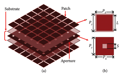
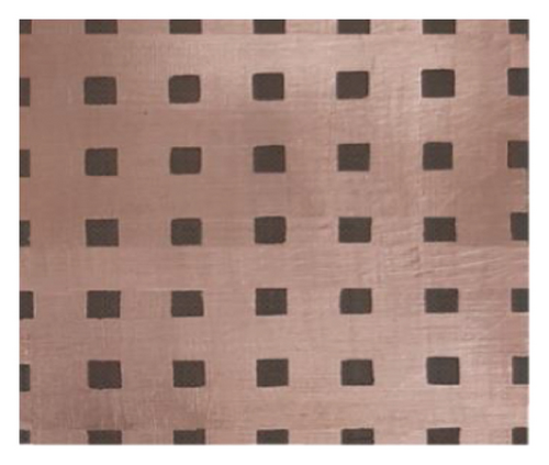
A FSS screen exhibiting bandpass filter response with the transmission coefficient near 0 dB at 5.5 GHz is required to be placed as a superstrate above the antenna. A patch-type FSS exhibits capacitance whereas aperture-type FSS exhibits inductance, so a combination of the two should form a parallel resonator with a transmission pole. The proposed multilayered FSS is composed of square-shaped patch-type layers with an aperture-type layer in between as can be seen from Figure 2(a). The FSS layers are based on 0.8 mm thick Arlon AD320 substrate whose dielectric constant is 3.2 and loss tangent is 0.002. Such a material of low loss is chosen to minimize the dielectric loss in the superstrate. The unit cell dimension for both patch- and aperture-type FSSs is Px × Py = 16 × 16 mm and the patch has a length of L = 13.8 mm with a spacing of 2.2 mm between the patches whereas the slot in the aperture-type FSS has a length of S = 3.7 mm as shown in Figure 2(b). The operation of the proposed multilayered FSS can be easily understood from an equivalent circuit model that can be constructed from transmission response of the individual FSS layers, as shown in Figure 3(a). In each case, the transmission response reveals nonresonant behaviour of the FSS at the operating frequency of 5.2 GHz. The simplified circuit in Figure 3(a) thus consists of two capacitors (Cp) and one inductor (La) [42]. The dielectric substrates between the FSS layers accounts for two short pieces of transmission line sections having impedances , where Z0 is the free space impedance = 377 Ω and εr = 3.2. Both ends of the circuit represents source and load having impedances Z01 = Z0r1 and Z02 = Z0r2, respectively, where r1 and r2 are normalized source and load impedances and for air, r1 = r2 = 1. The circuit can be modified with the transmission line sections represented by series inductance LS and shunt capacitance CS as shown in Figure 3(b). The T-network in this circuit can be converted to a π-network as shown in Figure 3(c), where two parallel resonators (L1C1 and L2C2) can be observed that are coupled via the inductor Lm.
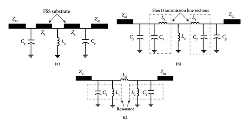
In the modified circuit, C1 and C2 both are parallel combination of Cp and CS. As can be seen from Figure 3(c), the circuit is basically a coupled resonator bandpass filter and this can be verified from the transmission response of the cascaded FSS.
2.3. Antenna–FSS Composite Structure
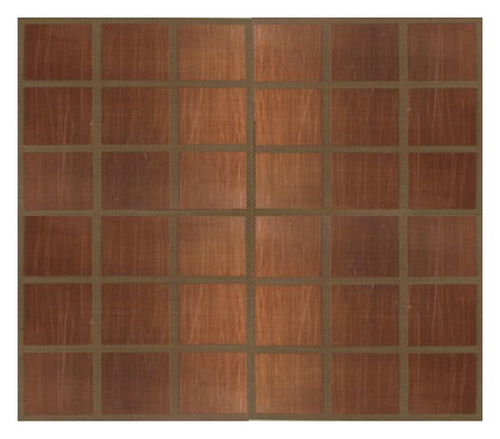
Three-layered frequency selective surface is placed over the SIW cavity-backed slotted antenna (Antenna-II) as superstrate to improve the radiation characteristics of the antenna. The three-layered structure designed and fabricated prototype along with the antenna structure is given in Figure 4.
3. Results and Discussion
The integrated antenna–FSS structure is developed and fabricated to function at a frequency of 5.42 GHz having narrow impedance bandwidth of 5.41–5.43 GHz.
3.1. Proposed Antenna Results
Parametric studies in terms of variation of reflection coefficient with changes in radius of the hexagonal split ring-shaped slot (r1, r2) and spacing between the open ends of slots (g1, g2) are performed on the proposed parent antenna designed to operate at a resonating frequency of 5.42 GHz in the TM010 dominant mode. Initially, the single split ring-shaped hexagonal slot is placed on the ground plane and the antenna (Antenna-I) now resonates at 5.52 GHz with an impedance bandwidth of 5.48–5.57 GHz. The plots for reflection coefficient variation with the alteration in radius (r1) and spacing between open ends of slot (g1) is shown in Figures 5(a) and 5(b), respectively. Figure 5(a) shows the deviation of reflection coefficient with respect to the radius and it depicts that as the radius varies from 6 to 8 mm, the results degrade, that is, for radius of 8 mm, the antenna’s reflection coefficient is even above −10 dB. Figure 5(b) depicted that the gap between the open ends of the split ring resulted in lower reflection coefficient for lesser gap ranging from 0.5 to 1.5 mm and as the gap was increased, the results improved for Antenna-I.
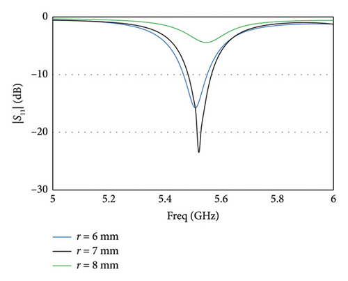
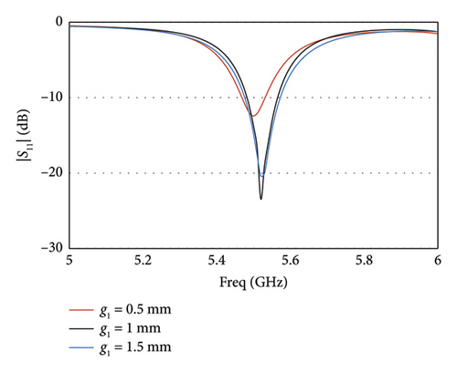
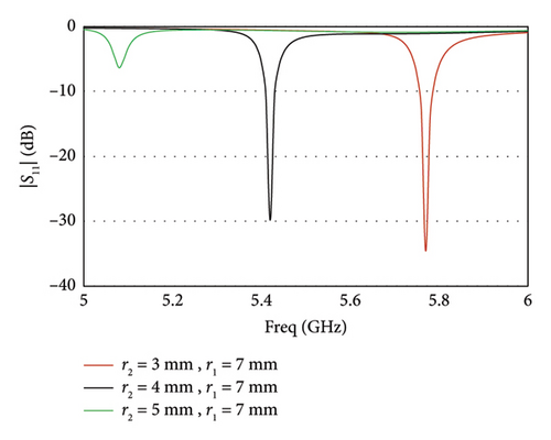
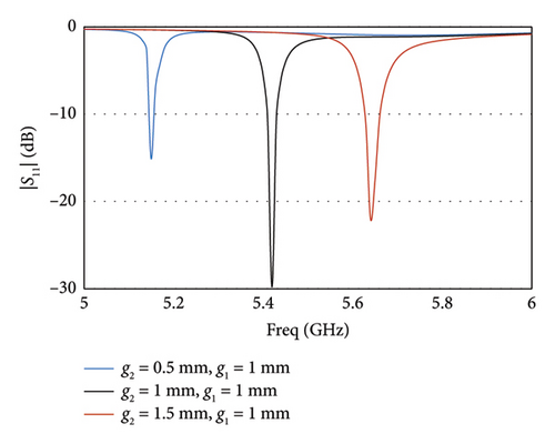
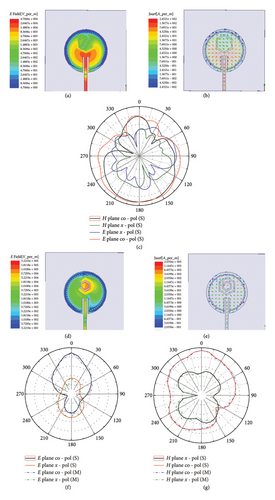
From the graphs, the best results are obtained for r1 = 7 mm and g1 = 1 mm. Reflection coefficient is simulated to be −23.4 dB at 5.42 GHz as shown in Figure 6(a). The simulated electric field copolarized antenna gain was 6 dBi, and the H-field copolarized gain was 5.8 dBi, as illustrated in Figure 7(c). The cross-polarised gains are found to be 20–30 dBi lower than their counterparts. Antenna-I design is modified with the inclusion of another hexagonal-shaped split ring slot on the patch and the radius (r2) and spacing between open ends (g2) are varied for best results with respect to reflection coefficient and gain of the antenna. The radius (r2) of the Antenna-II is altered from 0.5 to 1.5 mm, keeping radius (r1) fixed at 7 mm. It is seen from the graph in Figure 5(c) that as the radius of the inner slot on the patch is altered from 3 to 5 mm, there is a shift in frequency in the results. Though the reflection coefficient of −34 dB is obtained for r2 = 3 mm but at a frequency of 5.77 GHz which is far away from the resonating frequency of the Antenna-II while for the radius of 5 mm, antenna does not resonate. Thus, the best results are obtained for the radius of 4 mm, keeping r1 fixed at 7 mm. Figure 5(d) depicts the change of reflection coefficient with the change in gap between the open ends of the split ring-shaped slot from 0.5 to 1.5 mm, retaining the values of other parameters constant. It is seen that changing the dimensions results in frequency shift away from the operating frequency. Hence, the best result is g2 = 1 mm for Antenna-II.
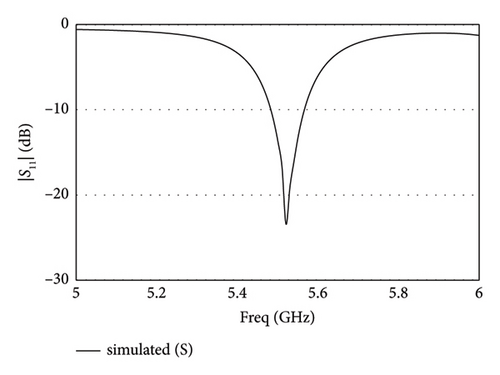
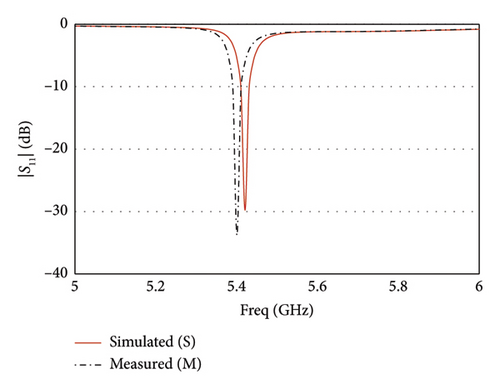
The simulated and measured reflection coefficients are obtained as −29.8 and −33.7 dB at 5.42 and 5.4 GHz, respectively, as given in Figure 6(b). The measurements are performed using Anritsu make VNA model MS205B. The modifications in the results occur due to the manufacturing intolerance in the material or the issues in SMA connector.
Electric field distribution for Antenna-I and Antenna-II are portrayed in Figures 7(a) and 7(d), respectively, at 5.52 GHz and 5.42 GHz in the fundamental mode while Figures 7(b) and 7(e) show the surface current distributions for both the antennas. The electric field copolarized simulated gain obtained is 7.2 dBi, while its measured value is 7.1 dBi at θ = 0° for 5.42 GHz in the TM010 mode. Similarly, the H-field cpolarised gains are found to be 7 dBi and 7.2 dBi at 5.42 GHz. Hittite HMC-T2100 microwave signal generator (10 MHz–20 GHz) and a Krytar 9000B power metre are used to measure the radiation characteristics for Antenna-II.
3.2. FSS Results
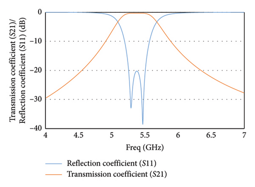
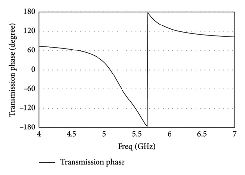
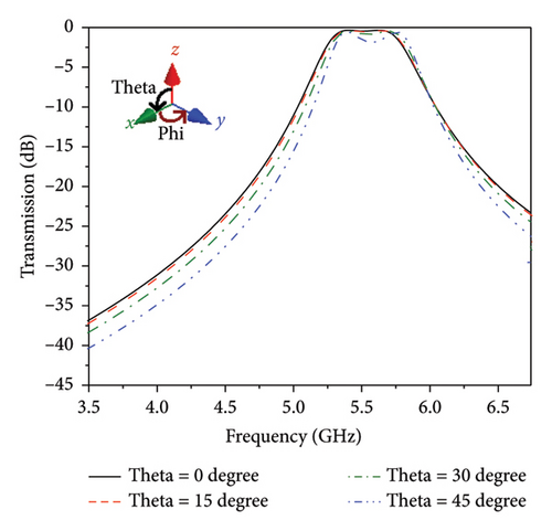
The characteristics of the FSS are investigated using ANSYS HFSS. Transmission as well as reflection characteristics of the FSS achieved using ANSYS HFSS are shown in the Figure 8(a). It can be observed from Figure 8(a) that the FSS exhibits a passband around 5.5 GHz with two closely spaced transmission poles at 5.4 and 5.6 GHz, for L = 13.8 mm. The electrical equivalent circuit of the FSS as shown in Figure 3 can be well justified from the characteristics, especially the transmission and reflection coefficient. Each transmission pole in the S21 response occurs due to one shunt LC resonator. As observed, the modified circuit in Figure 3(c) consists of two such LC resonators composed of L1, C1 and L2, C2 that are coupled via a mutual inductance Lm. These two LC resonators justify the occurrence of the two transmission poles at 5.4 and 5.6 GHz, resulting in the occurrence of the reflection zeroes at these two frequencies. The inductors L1, L2 and Lm are achieved by T to π network conversion from the combination of two Ls in the series path and one La in the shunt path. Thus, the presence of Ls and Cs is also justified. Moreover, Ls and Cs are representing the dielectric substrates. The insertion loss observed in the transmission response is controlled by this substrate material chosen. The closely spaced transmission poles in the characteristics that results in the desired passband justifies the significant coupling between the two shunt LC resonators through Lm. The FSS exhibits 3 dB bandwidth of 12% and an insertion loss of about 0.35 dB at the transmission poles, for L = 13.8 mm and S = 3.7 mm. Parametric studies are performed on FSS for better understanding of their behaviour. The transmission phase response is shown in the same plot and it varies linearly between 0° and −180°. All the parametric studies are performed for normal incidence of plane wave that is theta = 0°, so a study is carried out for oblique incidence. Transmission coefficients of the FSS for different values of theta are plotted in Figure 9 in the transverse electric (TE) plane (XZ plane), with electric field along y-axis. It is observed that the proposed design exhibits angular stability up to 45° with a small amount of addition in the insertion loss. The structure is symmetric with respect to linear polarization so the same studies are not performed in the transverse magnetic (TM) plane.
3.3. Antenna–FSS Composite Structure Results
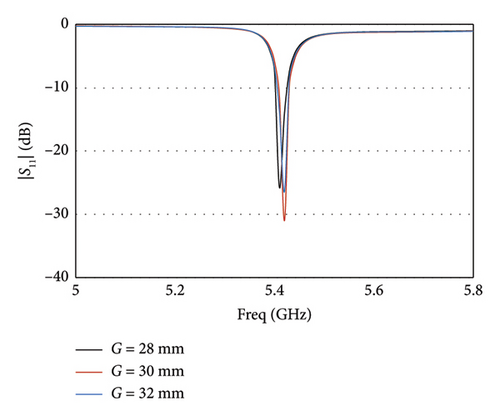
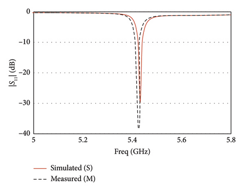
Parametric study is performed on the composite framework with respect to variation of the gap between antenna and FSS (G) for optimum results of reflection coefficient and gain. The optimized results are found at G = 30 mm as portrayed in Figure 10(a). The simulated and measured reflection coefficient for the composite structure is obtained as −31.01 dB at 5.42 GHz and −37.2 dB at 5.41 GHz respectively in the dominant TM010 mode. Figure 10(b) depicts a contrast in simulated and measured values. The slight variation in the reflection coefficient is caused by the reflection from the SMA connector or due to the manufacturing defects. Simulated and measured field patterns are given in Figure 11.
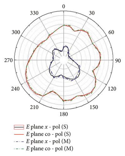
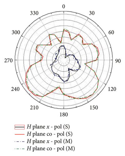
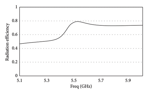
From the Figure 11(a), it is seen that the simulated E field co-polarised gain is 9.8 dBi while the measured result is obtained as 9.6 dBi at 5.42 GHz. Likewise, the H field simulated and measured copolarised gains are 9.6 and 9.4 dBi, respectively, at the same frequency of operation depicted in Figure 11(b). Their corresponding gain counterparts are below 20–30 dBi as compared with the copolarised gains. The isolation between the antenna and the FSS is maintained in order to ensure cancelation between the linearly decreasing transmission phase (Figure 8(b)) of the FSS and linearly increasing phase of rotational wave between antenna and FSS. The variation in isolation between antenna and FSS for adequate gain enhancement is performed that helps to choose an optimum isolation of 30 mm leading to an antenna gain of 9.8 dBi. Table 2 shows the complete study of reflection coefficients and gains for Antenna-I, Antenna-II and composite structure while the existing literature is compared with the proposed prototype in Table 3. Figure 12 portrays the graph of efficiency of the proposed design. It is seen that the radiation efficiency of the proposed structure is found to be 79.2%.
| Antenna type | Frequency (GHz) | Reflection coefficient (dB) | Impedance bandwidth (GHz) | Gain | |||||
|---|---|---|---|---|---|---|---|---|---|
| E field | H Field | ||||||||
| S | M | S | M | S | M | S | M | ||
| Antenna-I | 5.52 | — | −23.4 | — | 5.48–5.57 | 6 | — | 5.8 | — |
| Antenna-II | 5.42 | 5.4 | −29.8 | −33.7 | 5.40–5.43 | 7.2 | 7.1 | 7 | 7.2 |
| Antenna–FSS structure | 5.42 | 5.41 | −31.01 | −37.2 | 5.41–5.43 | 9.8 | 9.6 | 9.6 | 9.4 |
| Antenna–FSS structure | Substrate used | Frequency in GHz | Reflection coefficient in dB | Gain in dBi | Height in mm | Antenna area in mm2 |
|---|---|---|---|---|---|---|
| Patch antenna with FSS for dual-band antenna [26] | FR4 | 2.4/5.8 | −17/−25 | 7.9/8.1 | 35.3 | 40 × 40 |
| Patch antenna with bow tie-shaped slot with FSS [29] | FR4 | 4.2 | −23.51 | 4.20 | 1.59/3.14 | 30 × 30 |
| Patch antenna with dual polarization and FSS [30] | FR4 | 5.5 | Less than −10 | 17.7 | 35.2 | 106 × 106 |
| Triangular-shaped HMSIW antenna with superstrate of FSS [31] | Arlon AD270 | 6.5 | −31 | 8.7 | 22.6 | 60 × 60 |
| DRA antenna with FSS superstrate [32] | Arlon AD270 | 6.57 | −28 | 8.9 | — | — |
| Slotted SIW antenna with FSS [35] | Arlon AD270/Arlon AD320 | 5.38 | −32 | 7.1 | 28 | 60 × 60 |
| Proposed work | Arlon AD270/Arlon AD320 | 5.42 | −31.01 | 9.8 | 30 | 60 × 60 |
4. Conclusion
SIW-based circular cavity-backed antenna with hexagonal shaped slots on both the metallic surfaces and it operates at frequency of 5.42 GHz in U-NII-2B band for wireless communication. The hexagonal slot is initially placed on the ground surface and the antenna operates at 5.52 GHz with a gain of 6 dBi. Furthermore, the design is modified with the intrusion of hexagonal slot on the patch and now, the antenna resonates at 5.42 GHz with a gain of 7.1 dBi. Finally, the FSS is placed over the antenna structure and now, the antenna–FSS structure improves the gain to 9.8 dBi at 5.42 GHs. The proposed antenna, shielded by the FSS structure, is suitable for wireless communications near other conductors. It offers potential applications in various wireless networks, including WLAN, WiMAX, 5G Unlicensed band and marine radar. This antenna could be valuable for researchers worldwide seeking to integrate it with other electronic devices.
Conflicts of Interest
The authors declare no conflicts of interest.
Funding
The work was funded by University of Engineering and Management, Kolkata under the Grant-in-Aid project scheme (Project grant no. IEMT(N)/2024/A/08-G34).
Open Research
Data Availability Statement
The data used to support the findings of this study are available from the corresponding author upon reasonable request.


