Design and Performance Analysis of a Novel Asymmetrical Multilevel Inverter Structure With Reduced Components Using the Half-Height Modulation Technique
Abstract
This paper presents a novel single-phase 37-level asymmetrical multilevel inverter with fewer components and less voltage stress at the switches which reduces the cost of the inverter and increases efficiency. Existing multilevel inverters utilize a higher number of components to provide better output quality which increases the cost and the complexity. The proposed inverter circuit generates 37 levels of output voltage by utilizing only four DC sources and thirteen IGBT switches. Reduction of the total harmonic distortion (THD) and improvement of the output quality of the proposed structure are performed by implementing the half-height modulation technique. The number of components, cost factor, THD, and efficiency of the proposed structure have been compared to those of the inverter structures that are currently in use. The performance of the proposed structure is evaluated by MATLAB/Simulink and simulation results show that the proposed circuit produces higher-level output voltage with reduced THD by utilizing less components/levels and low-rated devices which makes the proposed topology cost-effective and efficient compared to other existing topologies. Also, the proposed structure offers stable performance under a variety of load conditions. Multiple input sources and less distorted output of the proposed topology make it appropriate for renewable energy generating systems which contribute to the reliable, efficient, and sustainable generation of electricity.
1. Introduction
In the growth of sustainable and reliable power systems, multilevel inverter (MLI) technology is essential as it meets the demands of power electronics’ applications. A MLI is such an inverter technology which produces an output voltage in the form of AC by taking several DC voltage levels at its input. By providing high-quality AC voltage with reduced harmonic distortion, MLIs become applicable in renewable energy systems [1], uninterruptible power supply systems [2], electric vehicles (EVs), high-voltage motor drives, and grid-tied inverters for distributed power generation [3]. Despite several advantages, conventional MLIs require a large number of components while producing more level of voltage at the output and face challenges related to switching losses, harmonic distortion, and higher stress on switches, which increases cost, reduces efficiency, and thus creates a hindrance to providing better performance for modern power systems [4, 5]. To overcome these issues, many research studies are being performed for meeting the requirements of diverse applications.
Flying capacitor (FC), neutral point clamped (NPC), and cascaded H-bridge (CHB) MLIs are the three commonly used conventional MLI topologies [6]. Of these, the CHB MLI structure has the additional advantage of not requiring any clamping diodes or capacitors and it provides high output voltage by cascading several single-phase converter modules which are simple in modular architecture [7]. CHB MLIs are categorized into two types viz. symmetrical and asymmetrical CHB MLIs. Symmetrical CHB MLIs possess the same magnitudes of the DC voltage sources, whereas asymmetrical CHB MLIs have unequal magnitudes of the DC voltage sources [8]. Besides this, in the case of asymmetrical CHB MLIs, the magnitude of the DC voltage sources can be selected in accordance with the need of achieving higher voltage levels [9]. While implementing a MLI structure, it is necessary to use a lower number of semiconductor devices for generating a higher level of voltage, which reduces the circuit complexity and thus increases the inverter’s reliability.
A single-phase asymmetrical MLI structure has been demonstrated in [10] for medium voltage application which uses twelve unidirectional switches and three DC sources for producing 23 levels of output voltage. However, employing additional gate driver circuits and switches brings about a rise in the inverter circuit’s cost. In [11], the presented topology is an asymmetric 21-level MLI which consists of ten unidirectional switches and three power sources. According to the required voltage level, it uses more switches and its switches also experience high-voltage stress due to the high total standing voltage (TSV) which are the disadvantages of this topology. Optimal utilization of the switching devices and voltage sources helps to simplify these issues. The authors in reference [12] present a new 17-level asymmetrical MLI which is applicable to photovoltaic systems. This MLI circuit has ten switches and four DC sources and 40% of its switches experience maximum voltage stress, which increases the inverter’s cost. Besides this, the total harmonic distortion (THD) of the output voltage is also high, that is, 7.78%. In [13], a novel 17-level CHB asymmetrical MLI architecture is described. It creates 17 different levels of output voltage through the use of two bidirectional and twelve unidirectional switches and four capacitors and four DC sources. However, the usage of more number of total components results in an increase in the inverter circuit’s cost. The same problem of increased cost for the use of more components while producing lower output voltage also exists in topologies [14, 15]. A 17-level MLI is built in [16] with an emphasis on component reduction and voltage boosting via switched-capacitor methods. Although the topology provides justifiable performance, its usefulness for high-voltage applications is limited by its greater THD (4.85%) and TSV (4.5 pu). Some MLIs which produce higher voltage levels at the output with less switches are presented in [17, 18]. These topologies use less switches while producing higher output voltage, so they are cost-effective for the usage of lower switches, but in [17], the output voltage has more harmonic contents with 2.53% of THD, and in [18], the topology of the switches experiences higher voltage stress. References [19–36] explore several new MLI circuits that utilize fewer switches and DC sources to provide a higher output voltage with lower THD, and the switches used in these circuits experience lower TSV. Modulation techniques such as unipolar trapezoidal pulse width modulation (PWM), carrier overlapping (CO), phase disposition (PD), alternative phase opposition and disposition (APOD), variable frequency (VF), and altered carrier PWM have been studied in various topologies [37, 38]. These approaches aim to reduce harmonics but often require complex control and are less scalable for high-level inverters, emphasizing the need for more simple and adaptable techniques. Self-balanced capacitor voltages, inherent voltage gain, and single DC source operation are some of the benefits of switched-capacitor MLIs (SC-MLIs) [39, 40]. However, these benefits come with significant challenges. Due to its high inrush current and current stress on switches and capacitors, SC-MLIs are only suitable for low- or medium-power applications. This results in higher power losses. To address inrush currents, additional components such as inductors are used, but this raises switching losses and overall circuit complexity [39]. Furthermore, under different load situations, performance decreases and complex control methods are needed to maintain capacitor voltage balance [40]. Although SC-MLIs are effective in certain applications, further study is required to develop inverter topologies that can operate efficiently at higher power ratings and with reduced switching losses. As the existing solutions do not meet the requirements of developing technologies, so novel MLI topologies are required to create higher output voltage with less components, reduced THD, and lower TSV. These features will decrease the cost of the MLIs and make it more efficient.
A novel 37-level asymmetrical MLI circuit is presented and designed in this work. The proposed topology uses lower components per level for generating higher output voltage with reduced THD, lower switching loss, and enhanced efficiency. Also, the proposed topology’s switches experience lower voltage stress which makes the inverter circuit cost-effective. MATLAB/Simulink is employed to simulate the proposed MLI structure. To assess the effectiveness of the proposed structure, its features are contrasted with those of a few other topologies. EVs and renewable energy generating systems find the proposed MLI convenient.
The rest of the paper is organized as follows. Section 2 describes the designed structure of the developed 37-level MLI circuit with design equations, its switching states, and modulation techniques. Features of the proposed MLI structure, voltage stress on switches, efficiency calculation, dynamic load variation effects and cost function determination are discussed in Section 3. In Section 4, a comparison of the proposed structure with a few existing structures and the detailed explanations of the graphical representations of the comparative analysis are presented. The application of the proposed topology is stated in Section 5. Finally, in Section 6, the conclusion and future scope are stated.
2. Proposed Inverter Circuit Configuration
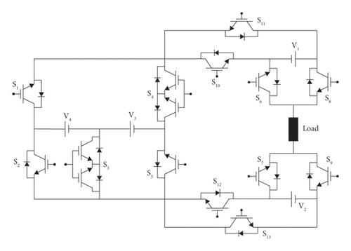
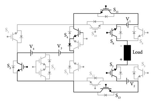
While designing the proposed 37-level MLI, various parameters should be considered to ensure the desired system’s performance, reliability, and efficiency. The proposed 37-level asymmetrical MLI circuit is shown in Figure 1, which consists of thirteen IGBT switches and four DC voltage sources. Among them, eleven switches, S1, S2, S5, S6, S7, S8, S9, S10, S11, S12, and S13, are unidirectional and two switches, S3 and S4, are bidirectional. This proposed 37-level MLI circuit can generate a stepped output waveform with 37 distinct voltage levels. With a VDC value of 22.22 V, the magnitudes of the DC sources, V1, V2, V3, and V4, are chosen in the proportion of 1:3:7:7 for the purpose of producing the required amount of output power. Under these circumstances, the proposed inverter circuit is capable of producing 18 positive voltage levels from +VDC to + 18 VDC, zero voltage level, and 18 negative voltage levels from −VDC to − 18 VDC.
2.1. Switching States of Operation of the Proposed Topology
MLIs operate in several switching states to produce the necessary output voltage waveform depending on the exact needs of the application. In this proposed 37-level asymmetrical inverter topology, there are thirty-seven operating states to generate 37 levels of output voltage. Table 1 shows switches’ switching patterns for producing different output voltage levels. The state value “1” indicates the conduction state of the switches, whereas the state value “0” specifies the nonconduction state. Based on the gate signals, six IGBT switches turn on each time, which are connected to respective voltage sources to create the different voltage levels.
| S1 | S2 | S3 | S4 | S5 | S6 | S7 | S8 | S9 | S10 | S11 | S12 | S13 | Vout | |
|---|---|---|---|---|---|---|---|---|---|---|---|---|---|---|
| Positive levels | 1 | 0 | 0 | 0 | 1 | 0 | 0 | 1 | 1 | 1 | 0 | 1 | 0 | 18 VDC |
| 1 | 0 | 0 | 0 | 1 | 1 | 0 | 0 | 1 | 1 | 0 | 1 | 0 | 17 VDC | |
| 1 | 0 | 0 | 0 | 1 | 1 | 0 | 0 | 1 | 0 | 1 | 1 | 0 | 16 VDC | |
| 1 | 0 | 0 | 0 | 1 | 0 | 1 | 1 | 0 | 1 | 0 | 1 | 0 | 15 VDC | |
| 1 | 0 | 0 | 0 | 1 | 1 | 1 | 0 | 0 | 1 | 0 | 1 | 0 | 14 VDC | |
| 1 | 0 | 0 | 0 | 1 | 1 | 1 | 0 | 0 | 0 | 1 | 1 | 0 | 13 VDC | |
| 1 | 0 | 0 | 0 | 1 | 0 | 1 | 1 | 0 | 1 | 0 | 0 | 1 | 12 VDC | |
| 1 | 0 | 1 | 0 | 0 | 0 | 0 | 1 | 1 | 1 | 0 | 1 | 0 | 11 VDC | |
| 1 | 0 | 1 | 0 | 0 | 1 | 0 | 0 | 1 | 1 | 0 | 1 | 0 | 10 VDC | |
| 1 | 0 | 1 | 0 | 0 | 1 | 0 | 0 | 1 | 0 | 1 | 1 | 0 | 9 VDC | |
| 1 | 0 | 1 | 0 | 0 | 0 | 1 | 1 | 0 | 1 | 0 | 1 | 0 | 8 VDC | |
| 1 | 0 | 1 | 0 | 0 | 1 | 1 | 0 | 0 | 1 | 0 | 1 | 0 | 7 VDC | |
| 1 | 0 | 1 | 0 | 0 | 1 | 1 | 0 | 0 | 0 | 1 | 1 | 0 | 6 VDC | |
| 1 | 0 | 1 | 0 | 0 | 0 | 1 | 1 | 0 | 1 | 0 | 0 | 1 | 5 VDC | |
| 0 | 0 | 0 | 1 | 1 | 0 | 0 | 1 | 1 | 1 | 0 | 1 | 0 | 4 VDC | |
| 0 | 0 | 0 | 1 | 1 | 1 | 0 | 0 | 1 | 1 | 0 | 1 | 0 | 3 VDC | |
| 0 | 0 | 0 | 1 | 1 | 1 | 0 | 0 | 1 | 0 | 1 | 1 | 0 | 2 VDC | |
| 0 | 0 | 0 | 1 | 1 | 0 | 1 | 1 | 0 | 1 | 0 | 1 | 0 | 1 VDC | |
| 0 | 0 | 0 | 1 | 1 | 1 | 1 | 0 | 0 | 1 | 0 | 1 | 0 | 0 | |
| Negative levels | 1 | 1 | 0 | 0 | 0 | 0 | 0 | 1 | 1 | 0 | 1 | 0 | 1 | 0 |
| 0 | 1 | 0 | 1 | 0 | 1 | 1 | 0 | 0 | 0 | 1 | 0 | 1 | −1 VDC | |
| 0 | 1 | 0 | 1 | 0 | 0 | 1 | 1 | 0 | 0 | 1 | 0 | 1 | −2 VDC | |
| 0 | 1 | 0 | 1 | 0 | 0 | 1 | 1 | 0 | 1 | 0 | 0 | 1 | −3 VDC | |
| 0 | 1 | 0 | 1 | 0 | 1 | 0 | 0 | 1 | 0 | 1 | 0 | 1 | −4 VDC | |
| 0 | 1 | 0 | 1 | 0 | 0 | 0 | 1 | 1 | 0 | 1 | 0 | 1 | −5 VDC | |
| 0 | 1 | 0 | 1 | 0 | 0 | 0 | 1 | 1 | 1 | 0 | 0 | 1 | −6 VDC | |
| 0 | 1 | 0 | 1 | 0 | 1 | 0 | 0 | 1 | 0 | 1 | 1 | 0 | −7 VDC | |
| 0 | 0 | 1 | 1 | 0 | 1 | 1 | 0 | 0 | 0 | 1 | 0 | 1 | −8 VDC | |
| 0 | 0 | 1 | 1 | 0 | 0 | 1 | 1 | 0 | 0 | 1 | 0 | 1 | −9 VDC | |
| 0 | 0 | 1 | 1 | 0 | 0 | 1 | 1 | 0 | 1 | 0 | 0 | 1 | −10 VDC | |
| 0 | 0 | 1 | 1 | 0 | 1 | 0 | 0 | 1 | 0 | 1 | 0 | 1 | −11 VDC | |
| 0 | 0 | 1 | 1 | 0 | 0 | 0 | 1 | 1 | 0 | 1 | 0 | 1 | −12 VDC | |
| 0 | 0 | 1 | 1 | 0 | 0 | 0 | 1 | 1 | 1 | 0 | 0 | 1 | −13 VDC | |
| 0 | 0 | 1 | 1 | 0 | 1 | 0 | 0 | 1 | 0 | 1 | 1 | 0 | −14 VDC | |
| 1 | 1 | 0 | 0 | 0 | 1 | 1 | 0 | 0 | 0 | 1 | 0 | 1 | −15 VDC | |
| 1 | 1 | 0 | 0 | 0 | 0 | 1 | 1 | 0 | 0 | 1 | 0 | 1 | −16 VDC | |
| 1 | 1 | 0 | 0 | 0 | 0 | 1 | 1 | 0 | 1 | 0 | 0 | 1 | −17 VDC | |
| 1 | 1 | 0 | 0 | 0 | 1 | 0 | 0 | 1 | 0 | 1 | 0 | 1 | −18 VDC | |
The proposed inverter system generates 37-level output voltages from −18 VDC to + 18VDC. The proposed 37-level MLI’s switching states define which IGBT switches and voltage sources are active to create particular output voltages from −18 VDC to + 18VDC. In each switching state, the current flow path can be determined by the connected voltage sources and the active switches. The IGBT switches include body diodes, which allow current to flow forward even when the switches are switched off. This enables smooth current flows and makes the switch protection possible, especially for circuits with inductive loads. In addition to providing a path channel for this current, the body diode protects from dangerous spikes that may damage the components. In this way, the body diode maintains the inverter functioning consistently.
Table 2 specifies the different states of switching for each switch with a load current flowing path. Among all the switching states, eight switching states are explained as follows.
| Switching states | Load current flow path | Output voltage |
|---|---|---|
| State-1 | S5 − V3 − V4 − S1 − S10 − V1 − S8 − Load − S9 − V2 − S12 | 18 VDC |
| State-2 | S5 − V3 − V4 − S1 − S10 − S6 − Load − S9 − V2 − S12 | 17 VDC |
| State-3 | S5 − V3 − V4 − S1 − S11 − V1 − S6 − Load − S9 − V2 − S12 | 16 VDC |
| State-4 | S5 − V3 − V4 − S1 − S10 − V1 − S8 − Load − S7 − S12 | 15 VDC |
| State-5 | S5 − V3 − V4 − S1 − S10 − S6 − Load − S7 − S12 | 14 VDC |
| State-6 | S5 − V3 − V4 − S1 − S11 − V1 − S6 − Load − S7 − S12 | 13 VDC |
| State-7 | S5 − V3 − V4 − S1 − S10 − V1 − S8 − Load − S7 − V2 − S13 | 12 VDC |
| State-8 | S3 − V4 − S1 − S10 − V1 − S8 − Load − S9 − V2 − S12 | 11 VDC |
| State-9 | S3 − V4 − S1 − S10 − S6 − Load − S9 − V2 − S12 | 10 VDC |
| State-10 | S3 − V4 − S1 − S11 − V1 − S6 − Load − S9 − V2 − S12 | 9 VDC |
| State-11 | S3 − V4 − S1 − S10 − V1 − S8 − Load − S7 − S12 | 8 VDC |
| State-12 | S3 − V4 − S1 − S10 − S6 − Load − S7 − S12 | 7 VDC |
| State-13 | S3 − V4 − S1 − S11 − V1 − S6 − Load − S7 − S12 | 6 VDC |
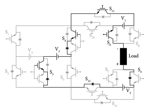
| State-14 | S3 − V4 − S1 − S10 − V1 − S8 − Load − S7 − V2 − S13 | 5 VDC |
| State-15 | S5 − S4 − S10 − V1 − S8 − Load − S9 − V2 − S12 | 4 VDC |
| State-16 | S5 − S4 − S10 − S6 − Load − S9 − V2 − S12 | 3 VDC |
| State-17 | S5 − S4 − S11 − V1 − S6 − Load − S9 − V2 − S12 | 2 VDC |
| State-18 | S5 − S4 − S10 − V1 − S8 − Load − S7 − S12 | 1 VDC |
| State-19 | S5 − S4 − S10 − S6 − Load − S7 − S12 | 0 |
| State-20 | S1 − S2 − S13 − S9 − Load − S8 − S11 | 0 |
| State-21 | S1 − S2 − S13 − S9 − Load − S6 − V1 − S11 | −1 VDC |
| State-22 | S1 − S2 − S13 − V2 − S7 − Load − S8 − V1 − S10 | −2 VDC |
| State-23 | S1 − S2 − S13 − V2 − S7 − Load − S8 − S11 | −3 VDC |
| State-24 | S1 − S2 − S13 − V2 − S7 − Load − S6 − V1 − S11 | −4 VDC |
| State-25 | S4 − V3 − S3 − S12 − V2 − S9 − Load − S6 − V1 − S11 | −5 VDC |
| State-26 | S4 − V3 − S3 − S13 − S9 − Load − S8 − V1 − S10 | −6 VDC |
| State-27 | S4 − V3 − S3 − S13 − S9 − Load − S8 − S11 | −7 VDC |
| State-28 | S4 − V3 − S3 − S13 − S9 − Load − S6 − V1 − S11 | −8 VDC |
| State-29 | S4 − V3 − S3 − S13 − V2 − S7 − Load − S8 − V1 − S10 | −9 VDC |
| State-30 | S4 − V3 − S3 − S13 − V2 − S7 − Load − S8 − S11 | −10 VDC |
| State-31 | S4 − V3 − S3 − S13 − V2 − S7 − Load − S6 − V1 − S11 | −11 VDC |
| State-32 | S4 − V3 − V4 − S2 − S12 − V2 − S9 − Load − S6 − V1 − S11 | −12 VDC |
| State-33 | S4 − V3 − V4 − S2 − S13 − S9 − Load − S8 − V1 − S10 | −13 VDC |
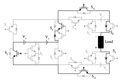
| State-34 | S4 − V3 − V4 − S2 − S13 − S9 − Load − S8 − S11 | −14 VDC |
| State-35 | S4 − V3 − V4 − S2 − S13 − S9 − Load − S6 − V1 − S11 | −15 VDC |
| State-36 | S4 − V3 − V4 − S2 − S13 − V2 − S7 − Load − S8 − V1 − S10 | −16 VDC |
| State-37 | S4 − V3 − V4 − S2 − S13 − V2 − S7 − Load − S8 − S11 | −17 VDC |
| State-38 | S4 − V3 − V4 − S2 − S13 − V2 − S7 − Load − S6 − V1 − S11 | −18 VDC |
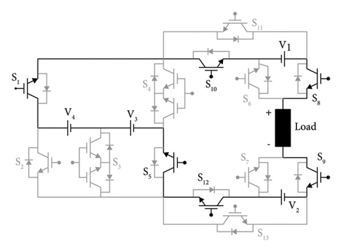
1st Switching state: S1, S5, S8, S9, S10, and S12 switches are kept active, while the remaining switches are left off during the first switching state. To provide an output of 18VDC, V1, V2, V3, and V4 voltage sources are also active with the switches S1, S5, S8, S9, S10, and S12. Figure 2(a) shows the current circulation path for this state.
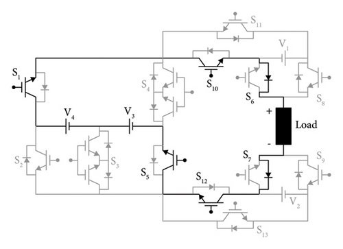
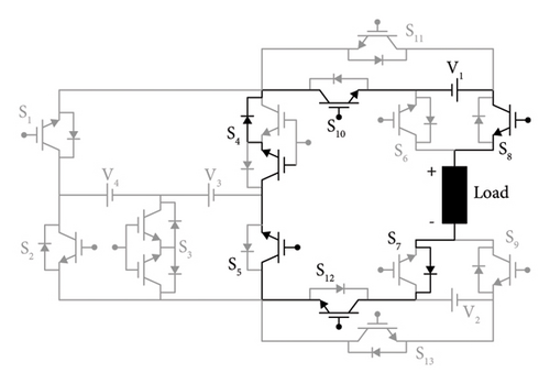
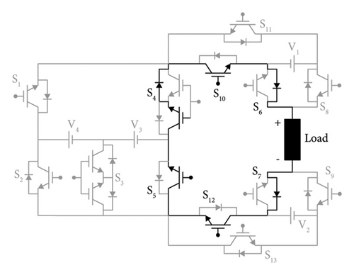
5th Switching state: S1, S5, S6, S7, S10, and S12 switches are kept active, while the remaining switches are left off during the fifth switching state. To provide an output of 14VDC, V3 and V4 voltage sources are also active with the switches S1, S5, S6, S7, S10, and S12. Figure 2(b) shows the current circulation path for this state.
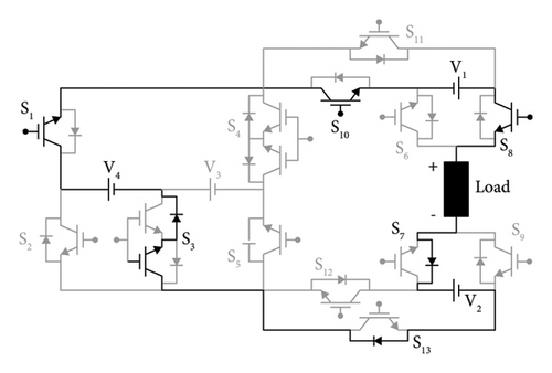
14th Switching state: S1, S3, S7, S8, S10, and S13 switches are kept active, while the remaining switches are left off during the 14th switching state. To provide an output of 5VDC, V1, V2, and V4 voltage sources are also active with the switches S1, S3, S7, S8, S10, and S13. Figure 2(c) shows the current circulation path for this state.
18th Switching state: S4, S5, S7, S8, S10, and S12 switches are kept active, while the remaining switches are left off during the 18th switching state. To provide an output of 1VDC, V1 voltage source is also active with the switches S4, S5, S7, S8, S10, and S12. Figure 2(d) shows the current circulation path for this state.
19th Switching state: S4, S5, S6, S7, S10, and S12 switches are kept active, while the remaining switches are left off during the 19th switching state. As no voltage source is active with S4, S5, S6, S7, S10, and S12 switches, there is no available path for the input voltage, so the output is zero. Figure 2(e) shows the current circulation path for this state.
25th Switching state: S3, S4, S6, S9, S11, and S12 switches are kept active, while the remaining switches are left off during the 25th switching state. To provide an output of −5VDC, V1, V2, and V3 voltage sources are also active with the switches S3, S4, S6, S9, S11, and S12. Figure 2(f) shows the current circulation path for this state.
34th Switching state: S2, S4, S8, S9, S11, and S13 switches are kept active, while the remaining switches are left off during the 34th switching state. To provide an output of −14VDC, V3 and V4 voltage sources are also active with the switches S2, S4, S8, S9, S11, and S13. Figure 2(g) shows the current circulation path for this state.
38th Switching state: S2, S4, S6, S7, S11, and S13 switches are kept active, while the remaining switches are left off during the 38th switching state. To provide an output of −18 VDC, V1, V2, V3, and V4 voltage sources are also active with the switches S2, S4, S6, S7, S11, and S13. Figure 2(h) shows the current circulation path for this state.
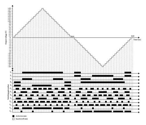
The typical 37-level staircase output waveform and the respective gate pulses are shown in Figure 3.
2.2. Design Equations of the Proposed 37-Level MLI Structure
A 37-level MLI structure is ingeniously designed to produce an output power of better quality while minimizing the number of components required. One of the standout features of this type of MLI is its ability to generate highly refined output with reduced THD, better voltage quality, and enhanced efficiency. The MLIs’ high-quality output power is essential to the systems that generate renewable energy. Various MLI topologies have some individual unique equations for representing their operation. These equations help in the determination of a number of components such as switches, sources, and gate driver circuits, which are essential to fulfill the necessary performance requirements.
2.3. Modulation Technique
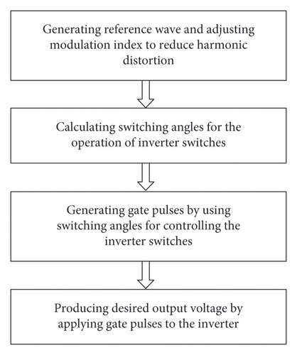
MLIs generate higher-level output voltage waveforms by using multiple levels of DC voltage. The half-height modulation technique is employed for creating output signals with low harmonic components for the proposed MLI structure. In this technique, a reference sine wave is generated and adjusted by fine-tuning the modulation index (MI) to ensure that the peak value of the reference sine wave is precisely half of the DC voltage level to minimize distortion. In order to control the inverter switches properly which are represented in Tables 3, 4, 5, and 6, the output waveform is then split into four quadrants for an entire cycle (0–360°) and switching angles are calculated by using the formulas [20] of equations (5)–(8) for each section. Finally, the gate pulses are applied to the inverter, which combines the DC voltage levels to produce a low-distortion AC output waveform that closely matches the reference sine wave. The entire process of the half-height modulation technique, including the calculation of switching angles, gate pulse generation, and output waveform creation, is illustrated in the flowchart shown in Figure 4.
| Symbol | Angle |
|---|---|
| A1 | 1.592 |
| A2 | 4.780 |
| A3 | 7.984 |
| A4 | 11.212 |
| A5 | 14.478 |
| A6 | 17.792 |
| A7 | 21.168 |
| A8 | 24.624 |
| A9 | 28.179 |
| A10 | 31.855 |
| A11 | 35.685 |
| A12 | 39.709 |
| A13 | 43.983 |
| A14 | 48.590 |
| A15 | 53.664 |
| A16 | 59.442 |
| A17 | 66.444 |
| A18 | 76.464 |
| Symbol | Angle |
|---|---|
| A19 | 103.536 |
| A20 | 113.556 |
| A21 | 120.558 |
| A22 | 126.336 |
| A23 | 131.410 |
| A24 | 136.017 |
| A25 | 140.291 |
| A26 | 144.315 |
| A27 | 148.145 |
| A28 | 151.821 |
| A29 | 155.376 |
| A30 | 158.832 |
| A31 | 162.208 |
| A32 | 165.522 |
| A33 | 168.788 |
| A34 | 172.016 |
| A35 | 175.220 |
| A36 | 178.408 |
| Symbol | Angle |
|---|---|
| A37 | 181.592 |
| A38 | 184.780 |
| A39 | 187.984 |
| A40 | 191.212 |
| A41 | 194.478 |
| A42 | 197.792 |
| A43 | 201.168 |
| A44 | 204.624 |
| A45 | 208.179 |
| A46 | 211.855 |
| A47 | 215.685 |
| A48 | 219.709 |
| A49 | 223.983 |
| A50 | 228.590 |
| A51 | 233.664 |
| A52 | 239.442 |
| A53 | 246.444 |
| A54 | 256.464 |
| Symbol | Angle |
|---|---|
| A55 | 283.536 |
| A56 | 293.556 |
| A57 | 300.558 |
| A58 | 306.336 |
| A59 | 311.410 |
| A60 | 316.017 |
| A61 | 320.291 |
| A62 | 324.315 |
| A63 | 328.145 |
| A64 | 331.821 |
| A65 | 335.376 |
| A66 | 338.832 |
| A67 | 342.208 |
| A68 | 345.522 |
| A69 | 348.788 |
| A70 | 352.016 |
| A71 | 355.220 |
| A72 | 358.408 |
In the half-height modulation technique, in order to determine the switching angles, the output waveform is split into four quadrants for an entire cycle (0–360°). Switching angles determined by the half-height modulation technique are represented in Tables 3, 4, 5, and 6. By using the formulas [20] of equations (5)–(8), the switching angles are computed.
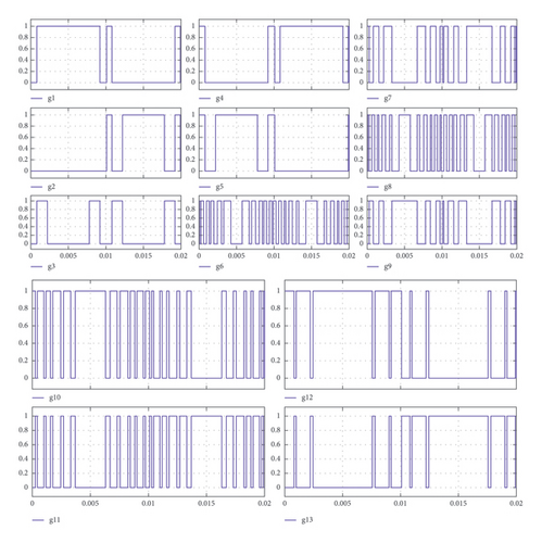
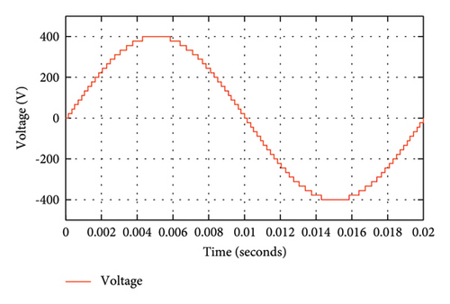
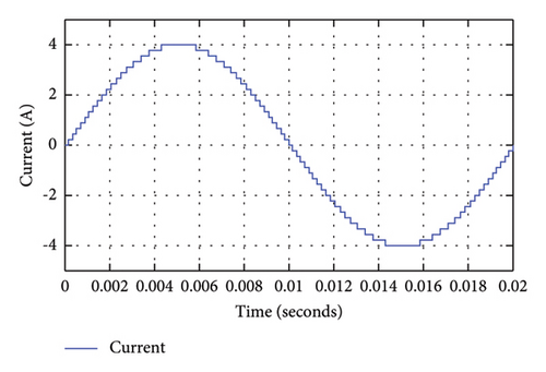
The gate pulses given to each of the switches to produce the required output through the half-height modulation technique are shown in Figure 5. In order to validate that the proposed circuit can generate 37 levels of voltage at the output, simulation is performed through MATLAB/Simulink using the half-height modulation technique. The voltage and current output waveforms of the proposed MLI circuit, determined by the simulation, are displayed in Figure 6.
3. Features of the Proposed MLI
Assessment of different features of a MLI is necessary while designing the inverter as it ensures that the inverter meets the requirements to function effectively. While assessing the proposed MLI, several features should be taken into consideration such as voltage stress across the switches, efficiency, and cost function of the proposed MLI as these features help to evaluate the overall performance and reliability of the proposed MLI. The following features are used to assess the effectiveness of the MLI.
3.1. Voltage Stress Estimation
To design and optimize a MLI, the knowledge of TSV is crucial, as TSV helps in selecting suitable switches with voltage ratings that can handle the maximum standing voltage, which ensures the reliability and longevity of the inverter and thus contributes to the overall efficiency and cost-effectiveness. TSV also helps in preventing damage to the inverter during abnormal operating conditions. Any inverter circuit’s cost is decreased by reducing the stress across switches.
The TSV is the total of each of the switch’s maximum voltage stresses. There are eleven unidirectional switches (S1, S2, S5, S6, S7, S8, S9, S10, S11, S12, and S13) and two bidirectional switches (S3 and S4) in the proposed MLI circuit.
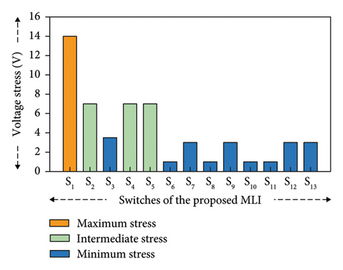
The amount of stress distribution can be represented by a term called normalized voltage stress (NVS). NVS refers to the voltage experienced by a component or a switch normalized to a reference value. It is the ratio of the actual voltage stress on a single switch to the maximum voltage stress on any switch in the circuit of a MLI. In the proposed MLI circuit, switch S1 experiences the maximum voltage stress among all the switches, which is 14 VDC. Thus, for the proposed MLI circuit, the NVS of all the switches is expressed in Table 7 and the stress distribution on the proposed MLI switches is expressed in Table 8
| Switches | Voltage stress on each switch | Maximum voltage stress among all the switches | Normalized voltage stress (NVS) calculation | Percentage of stress on switches (%) |
|---|---|---|---|---|
| S1 | 14 VDC | 14 VDC | 14 VDC/14 VDC | 100 |
| S2 | 7 VDC | 7 VDC/14 VDC | 50 | |
| S3 | 3.5 VDC | 3.5 VDC/14 VDC | 25 | |
| S4 | 7 VDC | 7 VDC/14 VDC | 50 | |
| S5 | 7 VDC | 7 VDC/14 VDC | 50 | |
| S6 | 1 VDC | 1 VDC/14 VDC | 7.14 | |
| S7 | 3 VDC | 3 VDC/14 VDC | 21.43 | |
| S8 | 1 VDC | 1 VDC/14 VDC | 7.14 | |
| S9 | 3 VDC | 3 VDC/14 VDC | 21.43 | |
| S10 | 1 VDC | 1 VDC/14 VDC | 7.14 | |
| S11 | 1 VDC | 1 VDC/14 VDC | 7.14 | |
| S12 | 3 VDC | 3 VDC/14 VDC | 21.43 | |
| S13 | 3 VDC | 3 VDC/14 VDC | 21.43 |
| Stress distribution | Switches | Percentage of switches under stress (%) |
|---|---|---|
| Maximum stress | S1 | 7.69 |
| Intermediate stress | S2, S4 , and S5 | 23.08 |
| Minimum stress | S3, S6, S7, S8, S9, S10, S11, S12, and S13 | 69.23 |
Different voltage stress levels experienced by the switches of the proposed MLI are represented in Figure 7. In this proposed MLI, switches S6, S8, S10, and S11 experience the lowest voltage stress among all the switches, which is 1VDC, and the lowest NVS, which is 7.14%. Switches S7, S9, S12, and S13 experience three times greater than the lowest stress among all the switches, which is 3 VDC, and NVS of 21.43%. The stress on the switch S3 is 3.5 VDC with a NVS of 25% which is much less than the intermediate NVS. Switches S2, S4, and S5 experience intermediate voltage stress which is 7 VDC and NVS of 50% which is exactly half of the maximum voltage stress and maximum NVS. Only one switch of the proposed MLI, S1, experiences the highest voltage stress of 14 VDC and a maximum NVS of 100%.
The percentage of switches under different stress levels is represented in Figure 8. The performance of a MLI circuit is greatly affected by the equal stress distribution on the switches, as in this situation, switches operate under similar conditions, which makes more efficient use of power, minimizes loss, and improves overall efficiency. Equal stress distribution on the switches of the MLI also helps to produce an output waveform with low harmonic distortion. So, achieving an equal voltage stress distribution is a key design consideration while designing a MLI. In this proposed MLI, although the voltage stress is not distributed in equal amounts among all the switches, 69.23% of the switches experience minimum voltage stress, 23.08% of switches experience intermediate stress, and only 7.69% of the switches experience high stress.
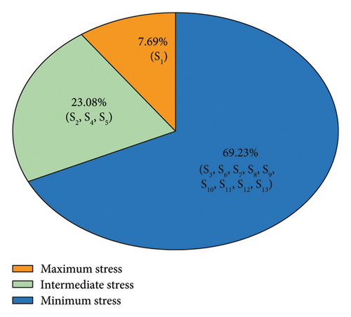
According to the voltage stress distribution throughout the switches, it is obtained that among the 13 switches of the proposed MLI, 9 switches experience less stress, 3 switches experience intermediate stress, and only one switch experiences maximum stress. The proposed MLI’s reduced voltage stress on switches results in low switching loss and low thermal stress which improves reliability, provides a longer lifespan for the switches, and thus leads to increased system efficiency. Besides this, reduced voltage stress–able switches are low voltage–rated switches, which potentially reduce the overall system cost.
3.2. Efficiency Calculation for Different Loads
Determination of the power losses of the inverter circuit is essential for calculating the efficiency of the MLI. Conduction and switching power losses are the two types of power losses which occur in the MLI topologies. IGBT of the model STGW60V60F is chosen as the power switch, and from the datasheet of the IGBT STGW60V60F, necessary values are obtained for calculating these power losses.
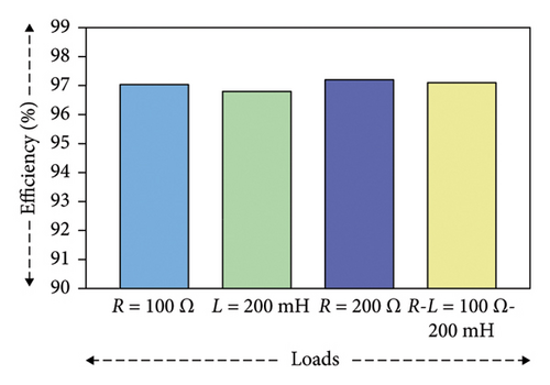
For different loads, the determined power loss and efficiency are tabulated in Table 9. With the change of loads, the variations of efficiency are shown in Figure 9. So, the improved efficiency of the proposed topology makes it increasingly attractive for various high-power and high-voltage applications.
| Parameters | Loads | |||
|---|---|---|---|---|
| R load (100 Ω) | L load (200 mH) | R load (200 Ω) | R-L load (100 Ω-200 mH) | |
| Vrms (V) | 282.84 | 282.84 | 282.84 | 282.84 |
| Irms (A) | 2.828 | 4.502 | 1.414 | 2.395 |
| Conduction losses, PC (W) | 1.88 | 3.17 | 0.894 | 1.57 |
| Turn on switching loss, Eon (W) | 0.005 | 0.008 | 0.003 | 0.004 |
| Turn off switching loss, Eoff (W) | 0.013 | 0.021 | 0.007 | 0.011 |
| Switching losses, PS (W) | 0.018 | 0.029 | 0.01 | 0.015 |
| Total losses, PT (W) | 24.67 | 41.59 | 11.75 | 20.61 |
| Output power, Pout (W) | 799.87 | 1273.35 | 399.94 | 677.40 |
| Input power, Pin (W) | 824.54 | 1314.94 | 411.69 | 698.01 |
| Efficiency, η (%) | 97.01 | 96.84 | 97.15 | 97.05 |
3.3. Cost Function Determination
The MLI’s cost function is a key consideration in its design, depending on the specific objectives of the application. Higher voltage level inverters usually require more components, such as switches, capacitors, diodes, and sources, and high voltage–rated devices increase the inverter’s cost. Besides this, the higher-quality components increase reliability and reduce maintenance and replacement costs over the inverters lifecycle. While designing a MLI, it should be taken into account that the inverter generates higher level voltage with less components and low-rated devices so that the reduction of cost of the inverter can be performed. That is why, the determination of cost function is most crucial.
3.4. Dynamic Load Variation Analysis
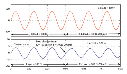
In order to evaluate the effectiveness of the proposed MLI structure in case of an abrupt load change, a dynamic load variation analysis is necessary. Figure 9 shows the dynamic load variation analysis of the proposed MLI structure. The inverter is initially loaded with a resistive load of R = 100 Ω, and in this condition, the output voltage obtained is 400 V and the output current is 4 A. After a while, the MLI is suddenly loaded with an inductor of value L = 200 mH, and as a result, the MLI feeds an R-L load of 100 Ω and 200 mH, which results in the same output voltage of 400 V, and the load current decreases to 3.38 A as shown in Figure 10(a).
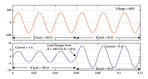
Furthermore, it can be seen from Figure 10(b) that the output voltage stays the same but the current rises to 8 A when the load resistance changes from R = 100 Ω to R = 50 Ω. Consequently, based on these findings it can be said that the proposed MLI structure’s output voltage remains constant even when the load varies. This is advantageous as it ensures a stable and reliable power supply for the connected load, and thus results in high-quality output power and a lower chance of damage to the equipment.
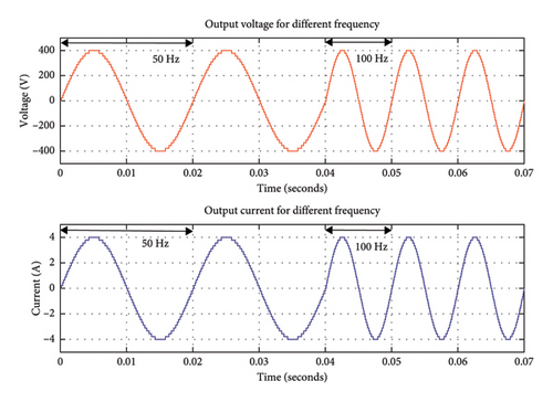
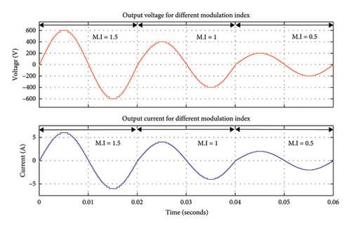
In addition, more dynamic tests for higher frequency applications, variations to the MI, and using nonlinear loads are also performed in order to determine the effectiveness of the proposed inverter. With the change of frequency from 50 Hz to 100 Hz, the output voltage remains the same as shown in Figure 10(c); however, due to the increase of the high-frequency switching losses, the THD of the MLI increases to 1.28%. In order to further investigate the effects of MI fluctuations, simulations with various MI values, ranging from 0.5 to 1.5, are conducted. Initially, the proposed inverter is loaded with a resistive load of R = 100 Ω. Under these conditions, the output voltage and current are 400 V and 4 A, respectively, with a MI of 1 and the THD obtained is 1.09%. With a higher MI of 1.5, the inverter continued to provide high-quality power with an acceptable THD of 1.53%, even though the output voltage (600V) and current (6A) were raised proportionally. Again, the output voltage (200 V) and current (2A) decrease proportionally at a lower MI of 0.5, but the inverter continues to perform well with a little increase in THD of 2.42%. Based on these findings, it can be observed that the proposed MLIs perform consistently over a wide range of MIs as shown in Figure 10(d).
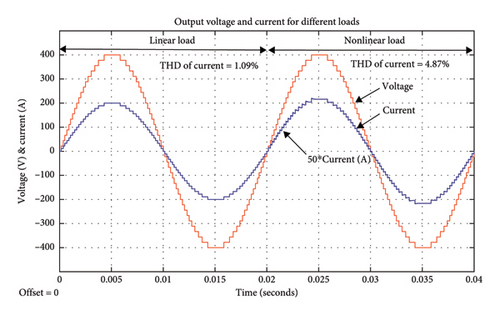
Again, from Figure 10(e), it can be seen that, with the change of load from linear load to nonlinear load (H-bridge diode rectifier), the output voltage waveform remains the same and it does not change its shape, but the shape of the output current waveform changes, which raises the THD (4.87%) due to the nonlinear nature of diode rectifier. As the proposed topology maintains a stable output voltage with low harmonic distortion, it reflects the proposed topology’s effective handling of nonlinear loads. These findings indicate that the proposed MLI is flexible in a variety of operating conditions and it provides excellent power quality despite the effects of changing frequency, MIs, and load conditions.
4. Comparative Analysis With the Existing MLI Topologies
To assess the proposed MLI circuit’s performance and determine whether it meets specific requirements for producing better results, a comparison of it is made with some existing MLI circuits currently in use. Depending on the number of components per voltage level, THD, cost factor per level, TSV, and efficiency, the proposed 37-level MLI structure is compared with several identical output voltage level topologies [27, 29] along with some varying output voltage level asymmetrical MLI topologies [19, 21, 23, 25, 31–36]. Table 10 outlines and displays the comparison variables required to perform a comparative evaluation of the proposed MLI structure with the structures that are currently in use.
| Topologies | Parameters | |||||||||||||
|---|---|---|---|---|---|---|---|---|---|---|---|---|---|---|
| NL | NDC | NSW | NGD | ND | NC | NDC/NL | NSW/NL | CC/NL | THD% | η (%) | TSV (pu) | CF/NL (α = 0.5) | CF/NL (α = 1.5) | |
| [31] | 21 | 2 | 11 | 11 | — | 5 | 0.10 | 0.52 | 1.38 | 3.67 | — | — | — | — |
| [32] | 21 | 3 | 10 | 6 | 2 | — | 0.14 | 0.48 | 1.00 | 3.99 | 95.7 | 2.45 | 1.06 | 1.18 |
| [33] | 27 | 3 | 11 | 11 | 2 | 4 | 0.11 | 0.41 | 1.15 | — | 97.28 | 5.3 | 3.5 | 4.1 |
| [34] | 51 | 2 | 8 | 8 | — | — | 0.04 | 0.16 | 0.35 | 1.17 | 96.98 | — | — | — |
| [35] | 31 | 6 | 10 | 10 | 6 | — | 0.19 | 0.32 | 1.03 | 1.82 | — | — | — | — |
| [36] | 31 | 4 | 10 | 10 | — | — | 0.13 | 0.32 | 0.77 | — | — | — | — | — |
| [19] | 31 | 4 | 14 | 14 | — | — | 0.13 | 0.45 | 1.03 | 3.32 | 92.32 | 2.4 | 1.07 | 1.15 |
| [21] | 33 | 4 | 12 | 12 | — | — | 0.12 | 0.36 | 0.85 | 2.03 | 94.10 | 3.31 | 3.11 | 3.51 |
| [23] | 35 | 6 | 12 | 12 | — | — | 0.17 | 0.34 | 0.86 | 1.9 | — | — | 1.74 | 3.51 |
| [25] | 35 | 5 | 12 | 12 | — | — | 0.14 | 0.34 | 0.83 | 1.88 | 93.37 | 3.2 | 1.6 | 3.18 |
| [27] | 37 | 6 | 13 | 13 | — | — | 0.16 | 0.35 | 0.86 | 3.64 | — | — | — | — |
| [29] | 37 | 10 | 12 | 12 | — | — | 0.27 | 0.32 | 0.92 | 1.98 | 97.2 | — | — | — |
| Proposed | 37 | 4 | 13 | 13 | — | — | 0.11 | 0.35 | 0.81 | 1.09 | 97.01 | 3.03 | 0.85 | 0.93 |
4.1. Number of Components Per Voltage Level
The number of components while designing a MLI is influenced by the output voltage level that the MLI is required to generate. To generate higher voltage levels, MLIs generally require higher components such as power semiconductor switches, gate drivers, diodes, capacitors, and DC sources. However, the higher number of components with high power–rated devices will make the designed inverters more costly and increase complexity. Figure 11 compares the suggested 37-level MLI with several MLI topologies. The number of components relies on the number of switches, gate drivers, diodes, capacitors, and DC sources. All of these features are taken into consideration while evaluating. The number of voltage levels obtained at the output by various inverter topologies is shown in Figure 11(d).
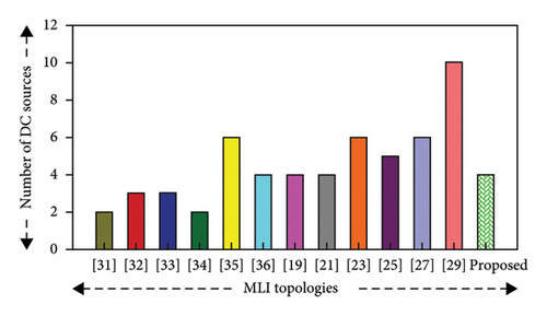
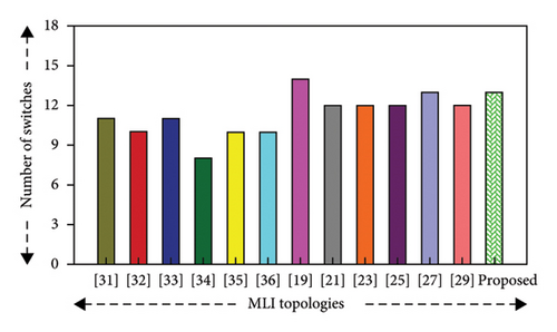
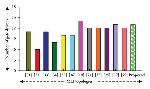
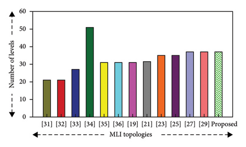
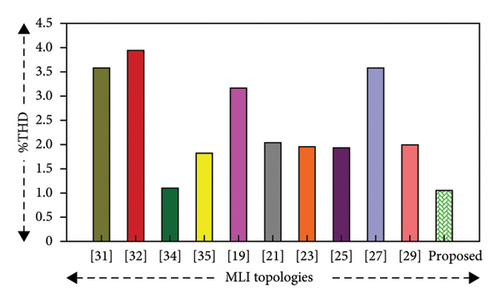
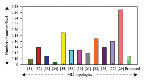
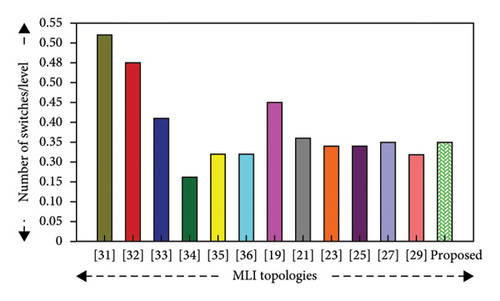
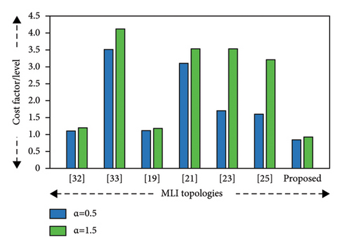
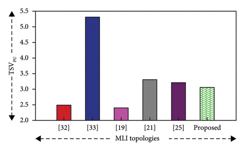
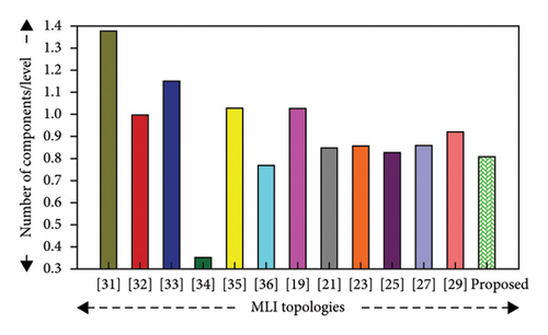
Table 10 illustrates that the proposed MLI structure utilizes less DC sources per level compared to the current topologies [19, 21, 23, 25, 27, 29, 32, 35, 36], although it produces a higher voltage level at the output, which influences the component count in the inverter, thus resulting in low cost. Although the voltage stress on the switches typically increases when the number of DC sources is reduced, this issue is effectively managed in the suggested circuit by using bidirectional switches. These switches reduce the voltage stress across the switches, which allows the use of low voltage–rated devices, so the cost and complexity are reduced. Although some topologies, such as [33, 36], require fewer sources/levels than the proposed topology, but in [33], switches suffer from high-voltage stress and [36] also introduce challenges related to voltage stress and control complexity by using only 2 DC sources producing 51 voltage level with an EPDB controller. The suggested MLI achieves a higher number of levels while using the same number of DC sources/levels as [32], indicating better utilization of available DC resources. On the other hand, in order to generate the same voltage level [27, 29], there is a need for more DC sources (6 and 10, respectively), whereas the suggested topology requires only 4.
The graphical representations of a number of sources and a number of sources/levels of the inverter topologies are shown in Figures 11(a) and 11(f), respectively.
Again, from Table 10, it can be seen that, while the proposed MLI uses slightly more switches per level than some topologies [23, 25, 29, 34–36], it still uses fewer switches/levels than others [19, 21, 31–33]. Even though the proposed MLI uses more switches per level compared to [23, 25, 29, 35], it requires fewer overall components per level. Besides this, although it [36] utilizes less components per level compared to the proposed topology, it produces a smaller number of voltage levels. On the other hand, although [34] it reduces hardware complexity by using less components while producing higher voltage levels than the proposed topology, using an EPDB controller to produce 51 levels shows challenges related to voltage stress and control complexity, which requires advanced computational resources to manage switching angles. So, the proposed topology is capable of producing higher voltage levels with fewer components, which offers more power without complicating the system.
The graphical representation of the number of switches, number of switches/level, and number of gate drivers of the MLI structure is shown in Figure 11(b), 11(c), and 11(g), respectively.
In order to show the improvements of the proposed design in comparison to the topologies which have comparable or closer output voltage levels such as [21] (33) and [25] (35), it can be found that the proposed topology achieves the highest number of voltage levels (37) while maintaining the same number of DC sources (4) as [21] and fewer than [25] (5). This results in a lower number of DC sources per level (NDC/NL = 0.11) compared to [21] (0.12) and [25] (0.14). Again, the proposed structure has switches per level (NSW/NL) of 0.35, which is less than [21] 0.36 and slightly higher than [25] 0.34, but this slight increase is balanced by achieving a reduced number of components per level (CC/NL = 0.81) compared to both [21] 0.85 and [25] 0.83. These enhancements indicate that the proposed topology is more efficient and less complex than existing topologies [21, 25] which emphasizes the novelty of the proposed MLI.
So, it can be observed from Table 10 that although the proposed MLI has a slightly higher number of switches/levels than some topologies, it requires less components/levels compared to all these existing topologies [19, 21, 23, 25, 27, 29, 31–33, 35] shown in Figure 11(j), which reduces the inverter’s overall cost. Besides this, MLIs with less components per level make the design of the topology simple which contributes to the improved reliability and ease of maintenance.
4.2. THD
The aim of the proposed MLI is to generate such an output voltage waveform which is closer to a sinusoidal waveform which means a waveform with reduced THD. THD is a measure of how much the waveform deviates from a perfect sine wave due to the presence of harmonics. Ideally, the output should be a pure sine wave with only the fundamental frequency, but in reality, inverters often generate additional frequencies known as harmonics. In order to reduce the amplitude of these higher-order harmonics, a half-height modulation technique is used in the proposed circuit which reduces half of the amplitude of the reference waveform. The fundamental frequency’s dominance and the suppression of higher-order harmonics confirm the MLI’s effectiveness in producing high-quality and efficient power, which is vital for renewable energy applications. The harmonic spectrum in Figure 12 demonstrates the effectiveness of the proposed MLI in reducing unwanted harmonics. The spectrum shows that these harmonics are significantly lower in amplitude compared to the fundamental frequency, indicating that the technique is effective and results in a very low THD.
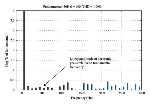
The need for 37 levels in our proposed asymmetrical MLI is to reduce THD and enhance the output waveform’s quality. The MLI with the higher number of voltage level might decrease harmonic distortion, but the actual THD depends on a number of factors, such as operating conditions, component parameter fluctuations, switching strategy, and more. With the same number of levels, different THDs of the MLIs can be obtained due to these factors. In addition, higher-level MLIs would need more components and make the design more complex and increase costs, whereas lower-level MLIs would result in higher THD and decreased power quality. The obtained THD of the proposed topology is compared with other existing topologies [19, 21, 23, 25, 27, 29, 31, 33, 34, 36], and it is obtained that the proposed MLI has the lowest THD value of 1.09%, which is better compared to all others, and is shown graphically in Figure 11(e). Topologies [23, 25] also have comparatively low THD values of 1.9% and 1.88%, respectively, but they still have higher distortion compared to the proposed MLI. Our designed 37-level MLI achieves a significant reduction in THD without requiring additional components as shown in Figure 11(j), which reduces system complexity and cost. Hence, the selection of the 37-level MLIs is appropriate as it provides the best possible balance between reducing THD, controlling system complexity, and maintaining low cost.
4.3. Cost Effectiveness
A MLI should be designed in such a way that it fulfills its required application with reduced cost. The proposed topology has a cost factor per level of 0.85 for a weight coefficient of α = 0.5 and 0.93 for α = 1.5, which is compared with other topologies [19, 21, 23, 25, 32, 33], and it was found to be less costly, which makes the proposed topology economically viable. The graphical representation of the cost factor/level of the inverter topologies is shown in Figure 11(h). Besides this, TSVpu also influences the cost by determining the voltage stress across switches as the rating of the switches depends on voltage stress. The proposed MLI structure has a TSVpu value of 3.03, which is less compared to the existing topologies [21, 25, 33], which indicates that the switches of the proposed topology experience lower voltage stress, so low-rated devices can be used; thus, it can be said that the proposed structure is cost-effective. Although the TSV of the proposed topology is more than [19, 32], it utilizes a lower number of components per level while generating 37 levels of output voltage with a reduced cost factor per level. So, in overall considerations, the proposed topology holds better results. The comparison is graphically represented in Figure 11(i).
4.4. Efficiency
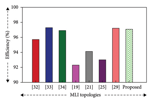
The proposed 37-level MLI optimizes a number of crucial features that impact MLI efficiency, such as switching losses, conduction losses, THD, and component count. As compared to other topologies in Table 10, the suggested MLI outperforms several existing designs, such as the topology in [19, 21, 25, 32, 34] with an efficiency of 97.01%. Although certain additional designs, including [29] (97.2%) and [33] (97.28%), provide similar efficiency, they do so with either a higher component count or increased THD. By lowering THD to just 1.09%, decreasing switching losses, and maintaining high efficiency with fewer components per level, the suggested MLI achieves an ideal balance. As seen in Table 9, where the losses are low even under varied load situations, this efficiency is further enhanced by decreased conduction and switching losses during power conversion. The efficiency of the proposed MLI is compared to different topologies in Figure 13, indicating its excellent balance between high efficiency, minimal THD, and optimal component utilization. Thus, the proposed MLI achieves improved utilization of energy, which increases its reliability and cost-effectiveness.
Thus, from the above mentioned comparisons, it can be said that the proposed structure generates 37 levels of output voltage by using a lower number of components per level with lower harmonic contents in the output of only 1.09% THD, reducing switching losses during power conversion, and the switches experience reduced voltage stress by better utilizing the DC voltage source. These features help to reduce the cost of the inverter and thus contribute to better efficiency of the MLI, which are the prominent benefits of the proposed MLI. So, in many applications including renewable energy generation systems, EV drives, and control of electric machines, the proposed MLI can be a replacement for conventional MLIs.
5. Application
The proposed asymmetrical MLI is particularly well-suited for applications in renewable energy systems and EVs. Renewable energy sources, such as solar panels and wind turbines, frequently provide DC voltage that fluctuates according to the atmosphere. This variable DC voltage may be converted at different voltage levels by MLIs into high-quality AC voltage. Since various voltage levels may be needed for transmission or distribution, this flexibility is essential for the efficient integration of renewable energy sources into the grid. Besides this, MLIs can operate at higher voltages. As a result, the system’s current flow is decreased, which lowers resistive losses (I2R losses) and increases efficiency. In addition, MLIs provide a number of benefits that make them suitable for EVs. Electrical components in EVs operate more smoothly because MLI reduces electromagnetic interference. MLIs’ compact scalable structural design not only reduces both weight and space but also allows for the integration of EVs with different power ratings and voltage requirements, which are important factors in the efficiency and performance of EVs. So, the proposed MLIs’ features, which include greater voltage capabilities, enhanced efficiency, less harmonics, scalability, and dependability, make it an excellent choice for renewable energy systems and EVs.
6. Conclusion
A novel asymmetrical MLI structure has been designed in this paper which utilizes less components/levels to produce 37-level output voltage. The distribution of the stresses on the switches of the proposed inverter is visualized in detail which shows that only 7.69% of switches experience maximum stress which results in the use of lower high-rated devices and thus the cost of the components of the inverter circuit gets reduced. A comparison is made to evaluate the performance of the proposed MLI with some current topologies on the basis of a number of components per voltage level, THD, TSV, cost factor per level, and efficiency. Comparison results show that the proposed structure generates 37 levels of output voltage using fewer components per level, which is significantly lower than that of conventional designs, ensuring less power losses. In addition, the reduction in component count minimizes design complexity and overall cost. The proposed MLI has less TSV (3.03 pu) and the cost factor is less as well which is 0.85 for α = 0.5 and 0.93 for α = 1.5 in comparison to other current topologies; thus, it can be said that the proposed structure is cost-effective. The MLI has been evaluated in dynamically loaded conditions and it is found to be stable overall. The half-height modulation technique is used for calculating the switching angles by which higher quality output waveform is achieved with a THD of 1.09%, which is much less compared to current topologies. These factors contribute to the MLI’s high system efficiency of 97.01%, which is one of the key benefits of the proposed design. Design and simulation of the proposed 37-level MLI have been performed in MATLAB/Simulink. In order to achieve better performance in the future, future research may involve developing an improved version of the proposed structure with fewer switches, lower THD, and less switch voltage stress with a higher level of voltage at the output. For EVs and renewable energy systems, the proposed MLI is excellently fitted.
Conflicts of Interest
The authors declare no conflicts of interest.
Funding
This research received no external funding.
Open Research
Data Availability Statement
The data that support the findings of this study are available from the corresponding author upon reasonable request.


