Volume 2025, Issue 1 2587682
Review Article
Open Access

Structural Analysis by X-Ray Diffraction Technique of Transition Metal Doped Zinc Oxide and Its Applications in Energy Storage Systems: A Critical Review

Hao Li

Hao Li

Energy Materials Research Group (EMRG) , School of Materials and Mineral Resources Engineering , Universiti Sains Malaysia , Pulau Pinang , Malaysia , usm.my

Key Laboratory of Micro-Nano Materials for Energy Storage and Conversion of Henan Province , College of Chemical and Materials Engineering , Institute of Surface Micro and Nano Materials , Xuchang University , Henan , China , xcu.edu.cn

Search for more papers by this author
Uzair Naeem

Uzair Naeem

Energy Materials Research Group (EMRG) , School of Materials and Mineral Resources Engineering , Universiti Sains Malaysia , Pulau Pinang , Malaysia , usm.my

Search for more papers by this author
Pin-Jiang Li

Pin-Jiang Li

Key Laboratory of Micro-Nano Materials for Energy Storage and Conversion of Henan Province , College of Chemical and Materials Engineering , Institute of Surface Micro and Nano Materials , Xuchang University , Henan , China , xcu.edu.cn

Search for more papers by this author
Li-Jun Wu

Li-Jun Wu

Key Laboratory of Micro-Nano Materials for Energy Storage and Conversion of Henan Province , College of Chemical and Materials Engineering , Institute of Surface Micro and Nano Materials , Xuchang University , Henan , China , xcu.edu.cn

Search for more papers by this author
Hong-Wei Yue

Hong-Wei Yue

Key Laboratory of Micro-Nano Materials for Energy Storage and Conversion of Henan Province , College of Chemical and Materials Engineering , Institute of Surface Micro and Nano Materials , Xuchang University , Henan , China , xcu.edu.cn

Search for more papers by this author
Adil Alshoaibi

Adil Alshoaibi

Department of Physics , College of Science , King Faisal University , Hofuf , Saudi Arabia , kfu.edu.sa

Search for more papers by this author
Dawei Wang

Dawei Wang

School of Instrumentation Science and Engineering , Harbin Institute of Technology , Harbin , China , hit.edu.cn

Search for more papers by this author
Bahri Deghfel

Bahri Deghfel

Department of Physics , Faculty of Sciences , University of Mohamed Boudiaf-M’Sila , M’Sila , Algeria , univ-usto.dz , s

Search for more papers by this author
Soorathep Kheawhom

Soorathep Kheawhom

Department of Chemical Engineering , Faculty of Engineering , Chulalongkorn University , Bangkok , Thailand , chula.ac.th

Search for more papers by this author
Ahmad Azmin Mohamad

Corresponding Author

Ahmad Azmin Mohamad

Energy Materials Research Group (EMRG) , School of Materials and Mineral Resources Engineering , Universiti Sains Malaysia , Pulau Pinang , Malaysia , usm.my

Search for more papers by this author
First published: 26 May 2025
Citations: 1
Academic Editor: Hu Li

Abstract

X-ray diffraction (XRD) is a versatile, nondestructive technique widely used for the analysis of crystalline materials. It provides detailed insights into structural characteristics, including phase identification, crystal orientation, grain size, crystallinity, strain, and defects. Zinc oxide (ZnO) demonstrates exceptional chemical and thermal stability as an n-type semiconductor, facilitating its use in applications such as supercapacitors, batteries, biosensors, photocatalysis, and medical devices. This review systematically examines recent advancements in the study of transition metals (TMs; e.g., Co, Fe, Mn, and Ni) doped ZnO materials for supercapacitors and lithium-ion batteries (LIBs). Emphasis is placed on employing XRD to explore how different dopants influence key structural parameters, such as lattice constants, grain size, defect concentration, and defect types. Through in situ XRD, real-time monitoring of structural changes is used to analyze the energy storage mechanisms, electrode optimization, and cycling performance of doped ZnO materials. The potential applications of co-doped ZnO and zinc-based high-entropy materials in energy storage are highlighted, providing valuable guidance for future research.

1. Introduction

The development of advanced energy storage systems is crucial for meeting the growing global energy demands and transitioning towards renewable energy sources. Among the various materials investigated for their potential applications in energy storage, zinc oxide (ZnO) has garnered significant attention due to its unique properties, such as high electron mobility, wide bandgap, and excellent chemical stability [13]. With the advancement of nanotechnology, various techniques such as sol–gel processing [47], magnetron sputtering [8, 9], electrochemical deposition [10, 11], and hydrothermal methods [1214] have been optimized to produce ZnO with desirable characteristics. These methods enable precise control of nanostructure properties, including particle size, shape, and surface area, which are critical for enhancing performance in energy storage devices.

In the field of energy storage, ZnO nanostructures have shown considerable promise, particularly in the development of supercapacitors and lithium-ion batteries (LIBs). Supercapacitors, renowned for their high power density, stability, and eco-friendliness, can significantly benefit from the incorporation of ZnO nanostructures [15, 16]. ZnO-based supercapacitors exhibit enhanced capacitance and cycling stability, especially when combined with other materials such as graphene and carbon. For instance, ZnO–graphene composites leverage the outstanding electrical conductivity and mechanical properties of graphene, resulting in superior supercapacitor performance [17, 18]. Similarly, ZnO–carbon materials, including carbon nanotubes and activated carbon, have been utilized to overcome the limitations of pure ZnO, such as volume expansion during electrochemical reactions and insufficient electrical conductivity [1921].

The integration of ZnO nanostructures into LIBs has garnered significant interest. LIBs are pivotal for numerous applications, including personal electronic devices, electric transport systems, and energy storage platforms, owing to their superior energy and power densities, long cycle life, and reliability [2225]. ZnO nanostructures, with their outstanding electrochemical characteristics and compatibility with other battery materials, have been explored to improve the efficiency of LIBs [2628]. The high surface area and distinctive electronic characteristics of ZnO nanostructures facilitation transport and storage efficiency, leading to improved battery capacity and stability.

ZnO has achieved significant advancements in supercapacitors and LIBs, substantially improving performance and sustainability. These developments have promoted energy storage technologies and facilitated the wider adoption of renewable energy. However, several critical challenges remain to be addressed. In supercapacitors, ZnO undergoes significant volume expansion during cycling, which induces mechanical stress and accelerates the electrode material degradation. Additionally, the relatively low electrical conductivity of ZnO limits its effectiveness in high-power density applications [2931]. In LIBs, although ZnO offers an outstanding theoretical capacity of 978 mAh g−1, it suffers from low intrinsic electrical conductivity and experiences significant volume changes during charge/discharge cycles [27, 32, 33]. Therefore, it is essential to improve not only the electrical conductivity of ZnO but also to increase the active sites and enhance mechanical stability to fully optimize its performance. The incorporation of ZnO with carbon materials or conductive polymers can enhance its conductivity; however, it also introduces nonactive materials, reducing the overall energy density. Despite the advantages of introducing a conductive phase, the combination of materials with different phases can lead to issues such as dense composition and high interfacial resistance. Additionally, defect engineering through mechanical treatment, thermal processing, or irradiation in the ZnO matrix can increase the specific surface area or enhance active sites [34, 35]. However, these methods often require specialized equipment, are costly, and have difficulties in controlling the defects. Moreover, excessive stress or high levels of defects may cause the ZnO structure to collapse.

To overcome these problems, doping ZnO with transition metals (TMs) has proven to be an effective strategy. TMs (e.g., Co, Fe, Mn, and Ni) play a pivotal role in enhancing the electrical conductivity and electrochemical performance of ZnO by introducing additional d-orbital energy levels [3639]. These dopants can provide extra redox-active sites, which boost the pseudocapacitive behavior of ZnO. Moreover, TMs doping can enhance the structural stability of ZnO, mitigating volume changes during charge–discharge cycles and improving cycling life and capacity retention. By optimizing the electronic and crystal structures of ZnO, TMs doping presents significant application potential, offering new insights for high-performance supercapacitors and batteries.

Comprehending the structural characteristics of ZnO is essential for optimizing its performance in various applications. To investigate the structure–performance relationship of TMs-doped ZnO in supercapacitors and batteries, key structural parameters must be examined. These include lattice parameters, doping concentration, stoichiometry, defect concentration and types, morphology, size, electrical conductivity, and band structure. X-ray diffraction (XRD) is a powerful analytical technique widely used to investigate the crystal structure, phase composition, and crystallite size of ZnO materials [40, 41]. This analysis method provides critical insights into the arrangement of atoms within the crystal lattice, which directly affects the physical and chemical properties of the material.

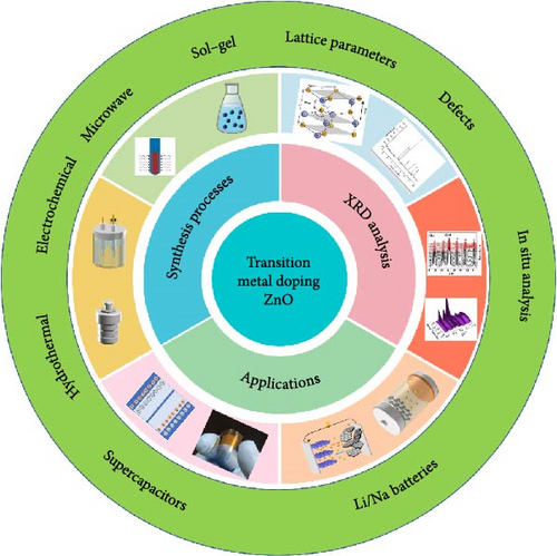
Previous reviews on doped ZnO have predominantly addressed applications in optics [42], photocatalysis [43], gas sensing [44], photoelectric conversion [45], and medicine [46]. However, reviews on doped ZnO in the field of energy storage are scarce, and the only available review concentrates on ZnO/carbon composites, as detailed in Khairundin et al. [47]. The present review systematically evaluates peer-reviewed studies (2015–2024) on TMs-doped ZnO for energy storage applications, with journal selection criteria emphasizing publications in impact factor >3.0 periodicals. Additionally, it emphasizes the application of XRD techniques in the structural analysis of doped ZnO and electrochemical analysis for energy storage. It covers various synthesis methods, the utilization of XRD techniques and other relevant aspects (Figure 1). The primary objectives are outlined as follows:
Details are in the caption following the image
Illustration of synthesis, XRD analysis, and applications of TMs-doped ZnO materials.
  • i.

    The role of XRD techniques in the analysis of TMs-doped ZnO will be thoroughly examined, focusing on the detection of critical parameters such as crystal structure, lattice constants, grain size, and defect analysis. Additionally, in situ XRD will enable real-time monitoring of structural changes, offering valuable insights into energy storage mechanisms, electrode design optimization, and the cycling performance of doped ZnO materials.

  • ii.

    Comprehensively summarize the research progress on TMs-doped ZnO, including single-ion doping and multi-ion co-doping techniques, for energy storage applications, with a specific focus on supercapacitors and LIBs. Furthermore, the potential application of zinc-containing high-entropy materials in energy storage will be introduced, emphasizing their significant promise for advancing the performance and development of supercapacitor and LIB technologies.

2. Detailed Analysis of XRD Measured Parameters

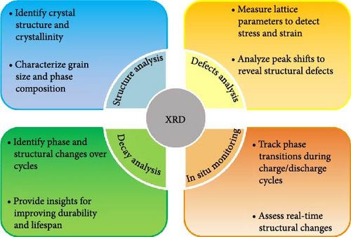
XRD is a critical tool in energy storage research, particularly for supercapacitors and batteries, enabling comprehensive material characterization. It provides essential insights into crystalline and nanostructural properties, including phase identification, grain size determination, and nanoscale features, foundational for optimizing electrochemical properties [48]. Its in situ monitoring capabilities allow real-time tracking of phase transitions and structural changes during charge/discharge cycles, which is crucial for designing stable and high-performance materials. Additionally, lattice parameter and stress–strain analysis via XRD reveal lattice variations, peak shifts, and stress effects that impact material performance and longevity [49]. Finally, XRD aids in degradation and failure mechanism analysis, uncovering irreversible phase changes and structural deterioration over cycles, supporting durability and lifespan improvements in energy storage devices (Figure 2). The significance of these parameters, their calculation processes, and their relevance to the field of energy storage will be discussed herein.
Details are in the caption following the image
Application of XRD in energy storage materials research.

2.1. Lattice Parameters

Analysis:
  • XRD provides valuable information about the crystal structure and lattice constants (a, b, c) by analyzing the angles and intensities of diffracted beams. To achieve this, the Bragg Law formula is utilized, which is expressed as Equation (1) [50, 51].

(1)

where n is the order of diffraction (usually 1), λ is the X-ray wavelength, d is the lattice spacing, and θ is the Bragg angle. This equation is essential for calculating the lattice spacing d. The lattice parameters of ZnO can be determined through XRD by measuring d value and combining it with the Miller indices.

Importance:
  • Changes in lattice parameters indicate the incorporation of dopants and the resultant strain in the crystal structure.

2.2. Crystallite Size

Analysis:
  • The Scherrer equation (Equation (2)) is an essential tool in XRD analysis for estimating the size of nanocrystals. It specifically measures the crystallite or particle size of materials by analyzing the broadening of diffraction peaks. The equation is expressed as follows [52, 53]:

(2)
where D is the average crystallite size, K is the shape factor, λ is the wavelength of X-ray, β corresponds to the full width at half maximum (FWHM) of the diffraction peak, and θ is the Bragg angle.
Importance:
  • Smaller crystallite sizes generally have higher surface areas, enhancing the electrochemical reactivity and overall performance.

2.3. Defect Concentration and Types

In addition to crystallite size, lattice strain plays a significant role in the broadening of XRD peaks, making it crucial to understand its impact. Since the Scherrer method does not consider the effects of strain, the Williamson–Hall (W–H) method is often employed to provide a more comprehensive analysis of both crystallite size and lattice strain.

Analysis:
  • Defects such as vacancies and interstitials cause peak broadening and shifts in XRD patterns.

  • The W–H (Equation (3)) can be used to separate size-induced and strain-induced broadening [54]:

(3)
where β is the FWHM of the peak, θ is the Bragg angle, K is the shape factor, λ is the X-ray wavelength, D is the average crystallite size, and ɛ is the microstrain.
Importance:
  • Quantifying defect concentration helps in understanding material imperfections that affect electrical and mechanical properties.

2.4. Doping Concentration

Analysis:
  • Doping changes the position and intensity of XRD peaks, and excessive doping concentrations can lead to the formation of secondary phases.

  • Shifts in peak positions can be correlated with changes in lattice parameters, which are influenced by the size and concentration of the dopant ions relative to host atoms.

Importance:
  • Understanding the doping concentration is critical for tailoring the electronic and ionic properties of the material to achieve its better performance.

2.5. Stoichiometry

Analysis:
  • XRD can detect phase purity and the presence of secondary phases, which arise due to deviations from the ideal stoichiometry.

  • The appearance of additional peaks in the diffraction pattern suggests the formation of compounds or phases with different stoichiometric ratios.

Importance:
  • Accurate stoichiometry is crucial for consistent electrochemical behavior and material stability.

While XRD provides critical insights into the structural parameters of TM-doped ZnO, such as lattice constants, crystallite size, and defect concentration, these parameters directly influence the electrochemical performance of ZnO-based energy storage devices. For instance, lattice strain induced by doping can enhance ion diffusion kinetics, while defect engineering can create additional active sites for redox reactions. In the following sections, how these XRD-derived structural characteristics translate into improved performance in supercapacitors and LIBs will be explored, with a focus on specific examples and mechanisms.

3. Pure ZnO Nanomaterials

3.1. Crystal Structure Analysis of Pure ZnO

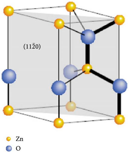
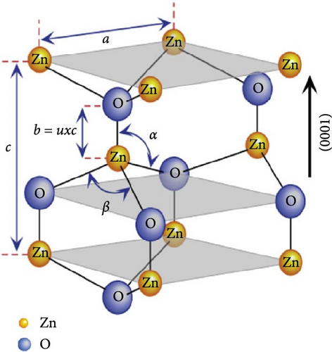
ZnO is a widely studied material that crystallizes in a hexagonal wurtzite structure under ambient pressure and temperature. This structure is characterized by two interpenetrating hexagonal close-packed (hcp) sublattices, each consisting of either Zn or O atoms, which are displaced relative to each other along the three-fold c-axis [55, 56]. The ZnO structure can be represented schematically as alternating layers of tetrahedrally coordinated Zn2+ and O2− ions arranged along the c-axis. The sp3 covalent bonding and tetrahedral coordination create polar symmetry along the hexagonal axis. This symmetry is a crucial factor affecting various ZnO properties, such as piezoelectricity, spontaneous polarization, crystal growth, etching behaviors, and defect generation (Figure 3a) [57].
Details are in the caption following the image
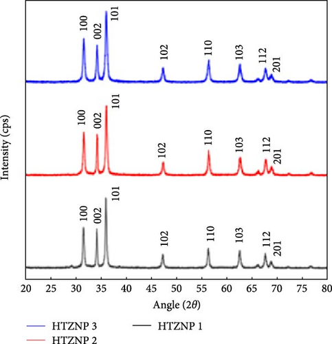
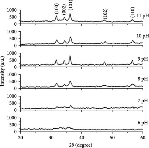
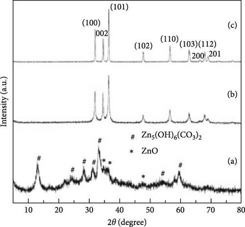
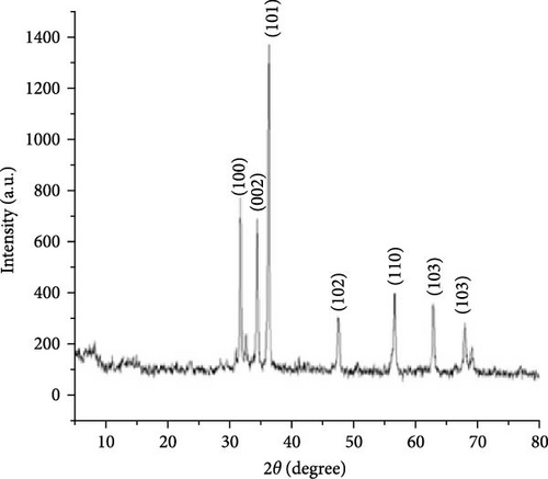
(a) ZnO wurtzite stick and ball structures, (b) schematic representation with lattice constants, reproduced with permission from [57]; (c) comparison of the main synthesis methods used for ZnO production, reproduced with permission from [58]; XRD patterns of samples obtained under different synthesis methods: (d) with different hydrothermal temperatures, reproduced with permission from [59]; (e) using sol having different pH value, reproduced with permission from [60]; (f) at 1 A dm−2 electrodeposited current density, reproduced with permission from [10]; and (g) eco-friendly synthesized ZnO-NPs, reproduced with permission from [61].

Additionally, the Zn–O bond exhibits significant ionic character, positioning ZnO on the borderline between covalent and ionic compounds, with an ionicity factor of fi = 0.616. The hexagonal unit cell of ZnO has lattice parameters of a = 3.2495 Å and c = 5.2069 Å, with a density of 5.605 g cm−3 (Figure 3b). This unique combination of structural, chemical, and physical properties makes ZnO an important material in various applications and a subject of extensive research [62].

Numerous physical, chemical, and biological methods for the synthesis of ZnO nanostructures have been thoroughly documented in the literature [52, 63, 64]. The primary preparation techniques for ZnO include electrochemical methods, hydrothermal methods, sol–gel processes, and biogenic approaches, each offering distinct advantages and limitations (Figure 3c) [58]. For example, hydrothermal methods offer significant advantages in controlling ZnO morphology and purity, but they often require high-temperature, high-pressure equipment and extended reaction times. In contrast, sol–gel processes operate under milder conditions but frequently involve toxic solvents and numerous side reactions. Therefore, researchers must select the most suitable preparation method based on the specific requirements of ZnO in their application field.

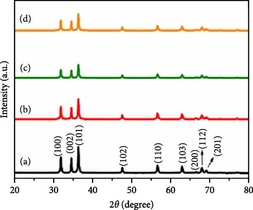
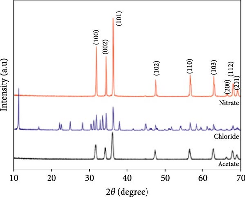
Regardless of the method chosen, XRD remains an indispensable analytical technique due to its speed, cost-efficiency, and effectiveness in analyzing ZnO crystallinity, particle size, and purity. For example, XRD analysis can quickly detect the purity and crystalline phase of ZnO. Strong diffraction peaks at 2θ values of 31.83, 34.42, 36.27, 47.48, 56.52, 62.70, and 66.81, correspond to the crystal planes of (100), (002), (101), (102), (110), (200), and (201) of the hexagonal wurtzite structure of ZnO, respectively [65, 66]. A few examples of XRD applications in the analysis of ZnO sample will be discussed herein.

The hydrothermal method, known for its simplicity and environmental safety, effectively tailors nanomaterial size and morphology [12, 59, 67]. ZnO powder was synthesized via a hydrothermal method to investigate the effects of temperature (100°C, 125°C, and 150°C) and duration (120 s, 1.3 h, and 5 h) on its structure. XRD analysis revealed that higher temperatures reduced the grain size, resulting in smaller and more crystalline particles (Figure 3d) [59]. Similarly, temperature-controlled synthesis (100°C–200°C) with citric acid revealed morphology transitions: hexagonal rods at 100°C, flower-like structures at 110°C–120°C, flake-like roses at 160°C and disordered nanosized plates above 180°C [68]. These findings underscore the importance of precise control during hydrothermal synthesis in optimizing ZnO nanostructures, as their morphology and crystalline properties directly influence the electrochemical performance of ZnO-based energy storage devices.

The sol–gel technique, renowned for its simplicity, low decomposition temperature, and adaptability in chemical composition, provides precise control over nanoparticle size and morphology. Its cost-effectiveness and scalability make it ideal for industrial production of high-quality crystalline nanostructures [4, 5, 69]. ZnO nanoparticles were synthesized using this method with different precursors, including zinc acetate dihydrate, oxalic acid, and ethanol in one study [70], and zinc 2-ethylhexanoate, ethylene glycol monomethyl ether, and isopropanol in another [71]. The choice of precursor chemistry plays a critical role in determining the morphology of the resulting ZnO nanoparticles. Additionally, pH significantly influences crystallinity, with XRD analysis revealing the optimal crystallite size (14 nm) and sharpest peaks at pH 9. At higher pH levels, rapid precipitation and dissolution reduce crystallinity, leading to a decline in material quality (Figure 3e) [60].

Electrosynthesis, utilizing a sacrificial zinc anode under controlled conditions, has gained prominence in the last decade. This top-down approach is now widely adopted for nanostructure preparation in various laboratories due to its effectiveness and versatility in using a solid precursor [10, 11, 72]. Nanosized ZnO particles were synthesized using an electrochemical-thermal method with NaHCO3 electrolyte, eliminating the need for zinc salts, templates, or surfactants. During electrolysis, Zn2+ ions produced at the sacrificial Zn electrode were subsequently converted into ZnO (Figure 3f) [10]. The indexed powder XRD pattern shows that the broadening of diffraction lines diminishes as the current density increases, indicating enhanced crystallinity of ZnO nanoparticles. At current densities of 0.5, 1.0, and 1.5 A dm−2, the average crystallite sizes are 18, 32, and 42 nm, respectively, highlighting the direct influence of current density on particle size and crystallinity.

In the last 15 years, biosynthesis of ZnO nanostructures has emerged as a cost-effective and environmentally friendly alternative to traditional methods. Phytogenic ZnO nanostructures are biocompatible and suitable for biological and environmental applications. The scalable process involves adding zinc salts to plant extracts, followed by a reaction period and thermal treatment, making it appealing for industrial and technological uses [61, 73, 74]. For example, ZnO nanoparticles were synthesized using aqueous fruit extracts of Myristica fragrans through an eco-friendly process [61]. XRD analysis confirmed the crystalline structure, revealing nanoscale particles with peaks at specific angles indicating high crystallinity (Figure 3g). The Scherrer formula calculated the crystallite sizes to be around 29 nm, with an average size of 41.23 nm. No impurities were detected, confirming the purity of the synthesized ZnO particles. In summary, advancements in various synthesis methods have laid the foundation for the widespread applications of ZnO and its modified materials.

3.2. Application in Supercapacitors

ZnO is regarded as a highly promising active material for supercapacitors, providing an impressive energy density of 650 Ah g−1 [75, 76]. This is attributed to its numerous advantages, such as low cost, abundant availability, environmental friendliness, and significant electrochemical activity. However, the applicability of ZnO as an electrode material for supercapacitors is limited by its low rate capability and poor reusability due to slow redox kinetics and high resistivity, affecting cycle performance and power density. These challenges can be addressed by integrating ZnO with various carbon materials, enhancing electrochemical capacitor performance.

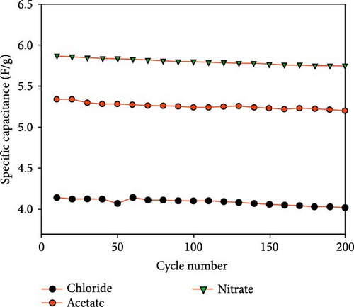
ZnO particles were synthesized via hydrothermal technique using zinc acetate, zinc chloride, and zinc nitrate precursors for supercapacitor electrodes [14]. XRD analysis revealed that ZnO from nitrate and acetate precursors has a hexagonal wurtzite structure, while those from chloride form a simonkolleite structure (Figure 4a). ZnO derived from nitrate exhibited superior crystalline quality and capacitance (5.87 F g−1) compared to those from acetate (5.35 F g−1) and chloride (4.14 F g−1), attributed to its larger specific surface area and smaller pores, which enhance electrolyte ion diffusion and capacitive performance (Figure 4b).
Details are in the caption following the image
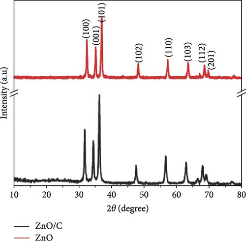
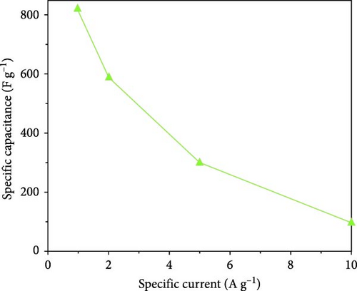
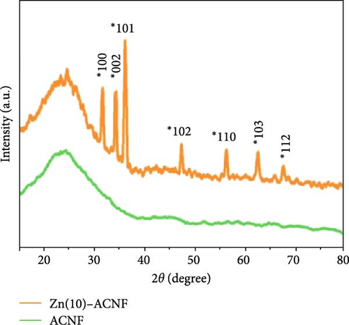
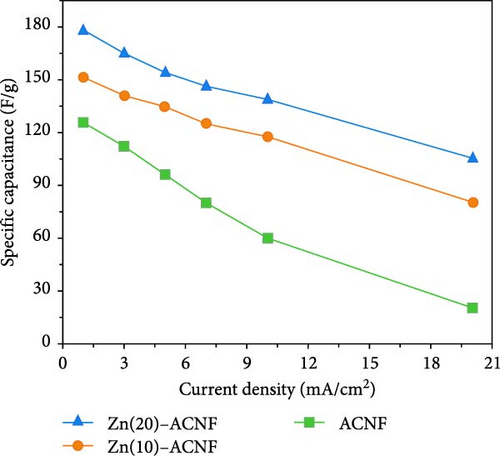
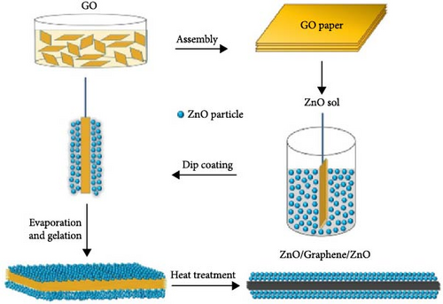
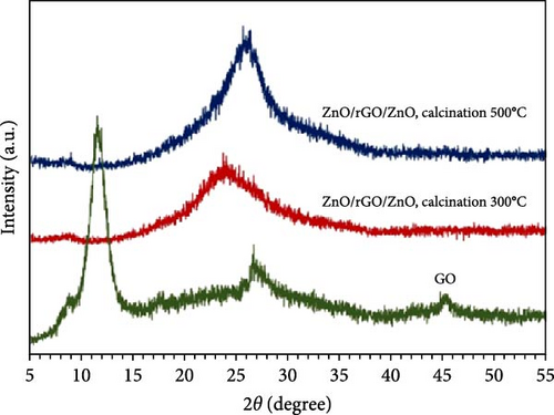
(a) XRD patterns and (b) cycling performance at a scan rate 5 mV s−1 of ZnO particles obtained at 140°C, reproduced with permission from [14]; (c) XRD patterns; (d) specific capacitance against applied current for ZnO/C electrode, reproduced with permission from [77]; (e) XRD patterns; (f) specific capacitances of Zn-ACNF and ACNF under different current densities, reproduced with permission from [21]; (g) schematic illustration of synthesis of sandwich ZnO/rGO/ZnO paper by dip coating method; and (h) XRD patterns of as prepared composites, reproduced with permission from [78].

A ZnO/C nanocomposite was synthesized via a sol–gel method, utilizing sucrose as a capping agent in accordance with green chemistry principles [77]. XRD analysis confirmed a hexagonal wurtzite structure with enhanced crystalline quality and an average grain size of 27.07 nm (Figure 4c). Electrochemical tests showed a maximum specific capacitance of 820 F·g−1 at 1 A·g−1, attributed to the composite’s optimized structural characteristics (Figure 4d). Similarly, ZnO/CNT nanocomposite electrode materials, fabricated using one-dimensional carbon nanotubes (CNTs), exhibited excellent capacitive performance [79]. These results indicate that the ZnO/C nanocomposite holds great promise as a high-performance supercapacitor electrode material, with significant potential for advancement in energy storage applications.

ZnO and activated carbon nanofiber composites (ZnO/ACNF) were synthesized via a single-step electrospinning method, utilizing polyacrylonitrile (PAN) in DMF with zinc acetate, followed by spontaneous sol–gel processing and physical activation [21]. XRD analysis confirmed the integration of ZnO and carbon nanofibers (CNFs), with Zn (10)-ACNF showing characteristic peaks of ZnO and disordered carbon (Figure 4e). Electrochemical analysis revealed Zn (20)-ACNF exhibited the highest capacitance due to synergistic effects between double-layer capacitance and redox reactions of ZnO (Figure 4f).

Developing flexible supercapacitors with improved energy and power densities is critical for advancing wearable electronics [80]. A cost-effective sol–gel method was developed to fabricate a freestanding sandwich-structured ZnO/rGO/ZnO paper electrode, with ZnO layers uniformly deposited on reduced graphene oxide (rGO) paper prepared via a modified Hummer’s method (Figure 4g) [78]. XRD analysis revealed effective GO reduction by ZnO and improved crystallinity at higher annealing temperatures (Figure 4h). The reduction mechanism involves Zn atoms reacting with oxygen functional groups on GO during heat treatment, forming ZnO. This process enhanced electrical conductivity by forming a conductive network within the ZnO/rGO/ZnO composites, essential for flexible supercapacitor performance. Similarly, CNT/ZnO/CNT composite electrodes were prepared via vacuum filtration, with the multilayer carbon structure enhancing conductivity and ensuring excellent electrochemical stability [81].

3.3. Application in Lithium Batteries

Due to its high theoretical capacity, strong chemical stability, and affordability, ZnO is regarded as a highly promising anode material for LIBs. There are three types of anode reactions in LIBs: intercalation, conversion, and alloying. Lithium storage in ZnO follows a reversible two-step process: the decomposition and formation of ZnO, along with the formation and decomposition of the Li–Zn alloy during discharge and charge cycles [26, 28, 32, 82, 83]. The specific reaction mechanism is described in Equations (4)–(6).

Conversion process:
(4)
Alloying–dealloying process:
(5)
Overall reaction:
(6)

Despite its excellent theoretical capacity of 978 mAh g−1, ZnO suffers from low intrinsic electrical conductivity and undergoes significant volume changes during charge and discharge processes. Compositing ZnO with various carbon materials effectively improves its conductivity and mitigates volume expansion [84].

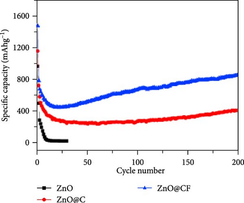
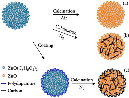
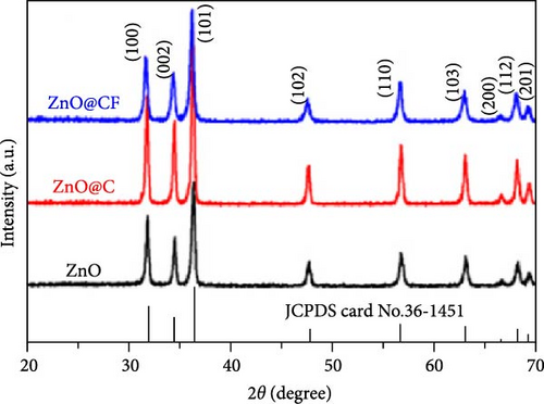
Three-dimensional (3D) ZnO structures, including microspheres, nanoflowers, and other complex architectures, exhibit diverse performance characteristics in LIBs, such as high specific surface area, excellent electrochemical conductivity, and good reversible capacity. ZnO nanoparticles enclosed in a 3D carbon framework (ZnO@CF) were prepared via a hydrothermal method followed by post-processing (Figure 5a) [83]. Dopamine coating and subsequent heat treatment in an N2 atmosphere decomposed zinc citrate into ZnO embedded in a carbon network, forming a 3D hierarchical structure. XRD analysis confirmed the hexagonal wurtzite ZnO phase and high crystallinity (Figure 5b). ZnO@CF electrodes achieved superior cycling stability, with reversible specific capacity increasing to 850 mAh g−1 after 200 cycles, outperforming ZnO@C (Figure 5c). Additionally, the core–shell and hollow ZnO/C microspheres were synthesized via a template-free method. Core-shell microspheres showed enhanced electrochemical performance due to their large surface area and internal voids, effectively mitigating active material deformation, slowing capacity fading, and extending battery lifespan [88].
Details are in the caption following the image
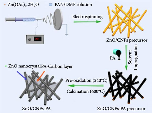
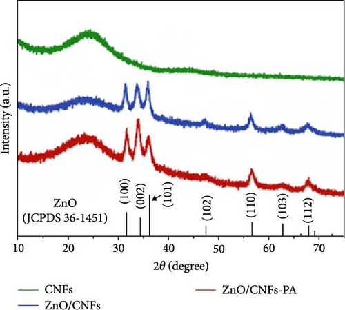
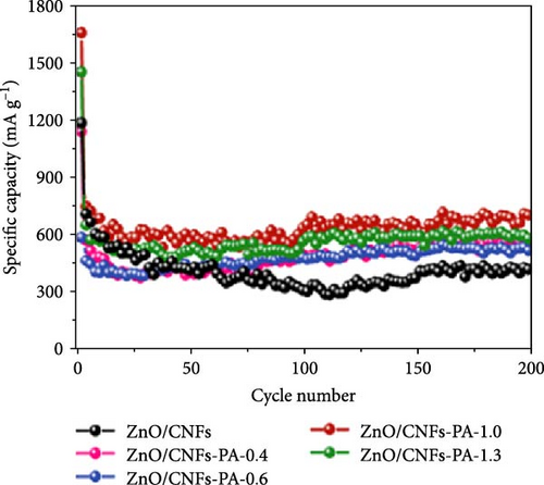
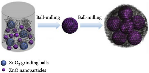
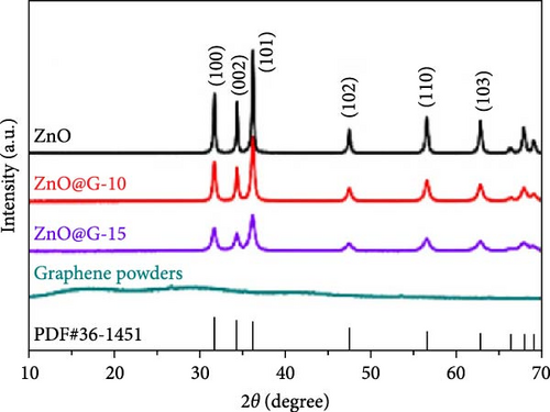
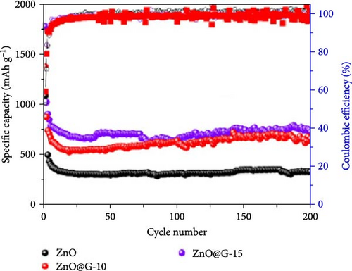
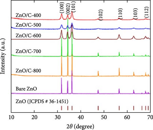
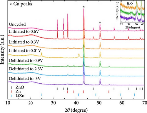
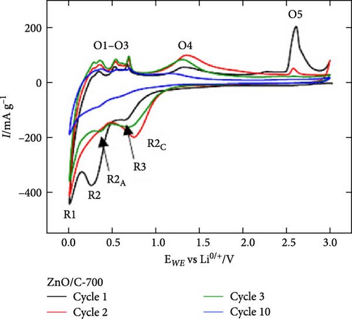
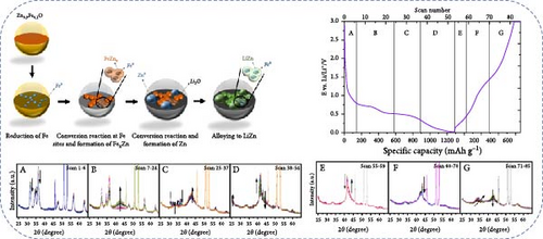
(a) Illustration for the synthesis of ZnO, ZnO@C, ZnO@CF, (b) corresponding XRD patterns, (c) cycle performance at the current of 0.1 A g−1, reproduced with permission from [83], (d) illustration for the synthesis of ZnO/CNFs-PA composites, (e) corresponding XRD patterns, (f) cyclic performance tests, reproduced with permission from [85], (g) illustration for the synthesis of ZnO@G by ball-milling method, (h) corresponding XRD patterns, (i) cycling stability at the current of 0.2 A g−1, reproduced with permission from [86], (j) XRD patterns of the ZnO/C composites, (k) ex situ XRD patterns of ZnO/C-700 electrode obtained at various stages of electrochemical Li+ in/desertion, and (l) CV of ZnO/C-700 at 0.1 mV s−1, reproduced with permission from [87].

Coupling nanostructured ZnO with 1D nanostructured CNFs not only buffers volume expansion but also improves electrical conductivity, thereby enhancing the overall electrochemical performance of the anode materials [89, 90]. Petroleum asphalt (PA) was used as the carbon processor, incorporated into ZnO/CNFs, followed by thermal treatments to form a 3D conductive network (Figure 5d) [85]. XRD analysis confirmed the average size of ZnO nanocrystals in the composites was around 17 nm, with the intercalation of PA not affecting the nanostructure (Figure 5e). Long-term performance evaluation revealed that ZnO/CNFs-PA electrodes maintained superior cycling stability and capacity, owing to the 3D network formed by the PA-based carbon layer (Figure 5f).

In recent years, two-dimensional (2D) nanomaterials have garnered significant interest due to their higher specific area and highly efficient planar channels, which facilitate lithium-ion transport. A ZnO-graphene composite (ZnO@G) was synthesized via a solid-state ball-milling method (Figure 5g) [86]. ZnO@G-10 and ZnO@G-15 exhibited sharp and intense peaks, indicating high crystallinity and reduced crystallite size, which decreased from 50 to 20 nm after ball milling (Figure 5h). Pristine ZnO electrodes experienced significant capacity decline to 323 mAh g−1 after 200 cycles due to pulverization caused by volume changes. Conversely, ZnO@G-15 electrodes maintained excellent cycling stability, retaining a capacity of 730 mAh g−1 after 200 cycles (Figure 5i). Additionally, a flexible ZnO/MXene film was developed via vacuum filtration to suppress lithium dendrite formation. ZnO nanoparticles reduced the nucleation barrier for lithium deposition while protecting the MXene substrate from degradation, demonstrating the potential of 2D materials in advanced LIBs technology [91].

Ex situ XRD, in situ XRD, and operando XRD techniques play crucial roles in LIBs research by revealing the crystal structure evolution of electrode materials at different cycling stages and dynamically monitoring changes during charge and discharge. For instance, in the study of ZnO/C composites, ex situ XRD showed that the ZnO/C-700 electrode retained the hexagonal ZnO phase without structural changes during solid electrolyte interphase (SEI) formation at 0.6 V. At 0.3 V, the ZnO phase transformed into Zn and Li2O, followed by the formation of the LiZn phase at 0.01 V. Upon charging to 0.9 V, the LiZn peak disappeared, and the Zn phase reappeared (Figure 5j–l) [87]. These findings provide direct evidence for the redox processes observed in CV, facilitating mechanistic studies. Furthermore, operando XRD was employed to investigate crystal structure changes in ZnO during SEI formation, providing deeper insights into reaction mechanisms [92]. These advanced techniques are invaluable for exploring performance optimization and understanding the reaction mechanisms of electrode materials.

4. Co-Doped ZnO Nanoparticles

4.1. Application in Supercapacitors

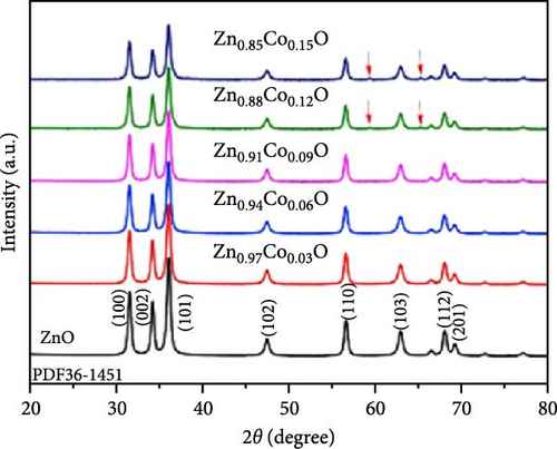
Because of the comparable ionic radius of Co2+ (0.72 Å) and Zn2+ (0.74 Å), Co ions can easily substitute at Zn interstitial sites, leading to high doping concentrations in the ZnO crystal structure. Zn1−xCoxO samples with nominal Co concentrations (1, 3, 5, 7, and 9 at.%) were synthesized using a conventional solid-state reaction technique (Figure 6a) [34]. The XRD patterns of the samples, displayed on a logarithmic scale to emphasize potential secondary phases, show only peaks corresponding to the wurtzite ZnO structure. Within the sensitivity range of the applied technique, these results suggest the absence of secondary phases and confirm the successful integration of dopants into the ZnO lattice.
Details are in the caption following the image
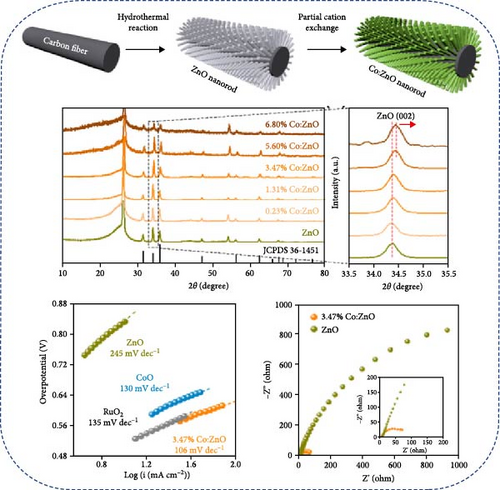
(a) XRD pattern of Zn1−xCoxO samples with different Co doping content, reproduced with permission from [34]; (b) schematic illustration, XRD patterns of Co/ZnO with various Co doping ratios, corresponding tafel slopes and electrochemical impedance spectroscopy (EIS), reproduced with permission from [93]; (c) XRD patterns of pristine ZnO and Co-doped ZnO; (d) CV of ZnO-based samples, reproduced with permission from [94]; (e) XRD patterns of pure and Co/ZnO nanoparticles; (f) enlarged view of (101) peak; and (g) galvanostatic charge/discharge (GCD) profiles at a current density of 1 A g−1, reproduced with permission from [95].

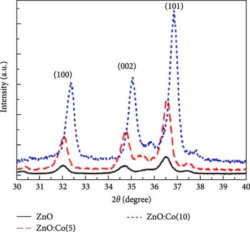
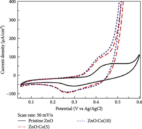
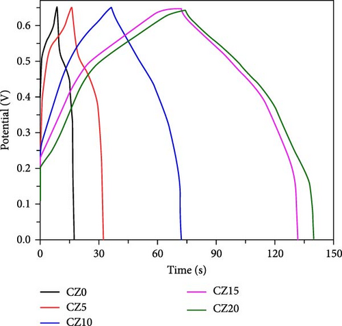
Co-doped ZnO materials exhibit excellent electrochemical catalytic and capacitive performance. Co-doped ZnO nanofibers were synthesized via a hydrothermal method followed by partial cation exchange (Figure 6b) [93]. XRD analysis confirmed that all Co/ZnO and ZnO samples exhibited a hexagonal ZnO structure. Increased Co doping caused the (002) diffraction peak to shift to higher angles, indicating minor lattice compression due to the smaller ionic radius of Co ions. The 3.47% Co/ZnO sample demonstrated superior catalytic activity compared to CoO and RuO2. Furthermore, Co-doped ZnO nanomaterials synthesized via chemical co-precipitation were employed as supercapacitor electrodes [94]. XRD analysis revealed an average grain size of 17–19 nm, with increasing Co content slightly enlarging grain size and shifting XRD peaks to higher angles. Cyclic voltammetry showed that Co-doped materials exhibited higher current density and enhanced electrochemical response speed at high scan rates (Figure 6c,d).

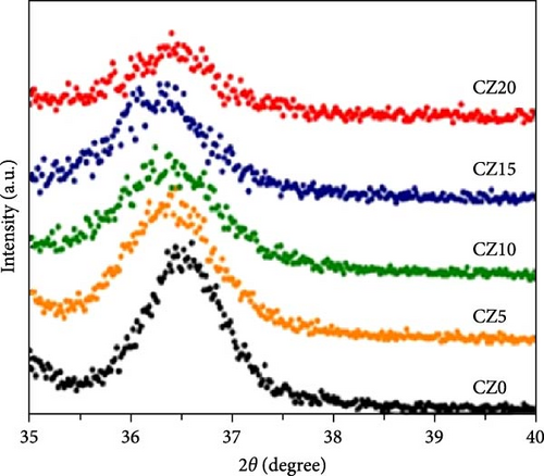
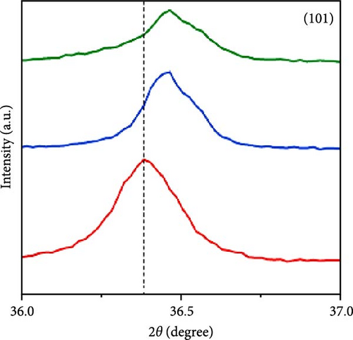
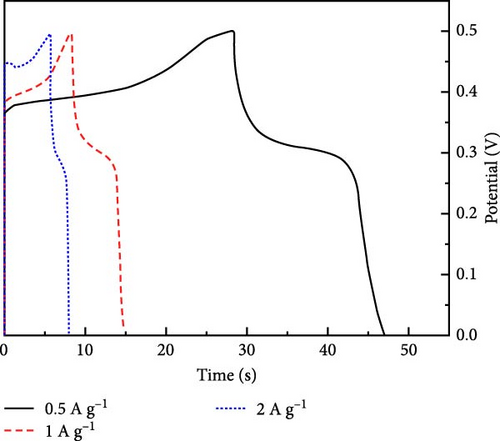
Co doping introduces Zn vacancies and polarons into the ZnO lattice, significantly enhancing its capacitance performance. Co-doped ZnO nanoparticles were synthesized via a low-temperature co-precipitation method, with XRD analysis confirming a wurtzite structure across all compositions (Figure 6e) [95]. Increased Co concentration caused a decrease and broadening of the (101) plane peak, indicating reduced crystallite size and distorted crystalline quality (Figure 6f). The ZnO electrode doped with 20 at.% Co exhibited a specific capacitance of 104.46 F g−1, significantly higher than the 13.23 F g−1 of pristine ZnO due to polarons and Zn vacancies (Figure 6g). ZnO quantum dots (ZnO QDs) further enhance performance through a high surface-to-volume ratio, reduced ion diffusion lengths, and quantum confinement effects. Zn1–xCoxO QDs (x = 0, 0.02, 0.04) synthesized via wet precipitation showed improved specific capacitance [96]. At 1 A g−1, Zn0.96Co0.04O achieved a specific capacitance of 697 F g−1, outperforming pristine ZnO (416 F g−1) and Zn0.98Co0.02O (554 F g−1).

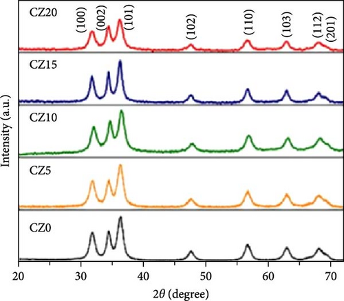
Unveroglu Abdioglu [94] demonstrated that increasing Co content reduces lattice parameters and volume, evident from XRD peak shifts to higher angles and an average crystallite size of 17–19 nm. Conversely, Ponnusamy et al. [95] reported that Co doping induced microstrain, zinc vacancies, and polaron formation, causing localized lattice expansion and smaller crystallite sizes of 6–10 nm. While one study identified 5 at.% as optimal for balancing conductivity and stability, the other achieved superior results at 20 at.% through defect engineering. Future research should standardize protocols and employ advanced techniques to clarify defect-structure relationships and optimize Co-doped ZnO for energy storage.

4.2. Application in Lithium Batteries

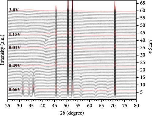
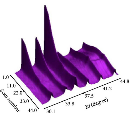
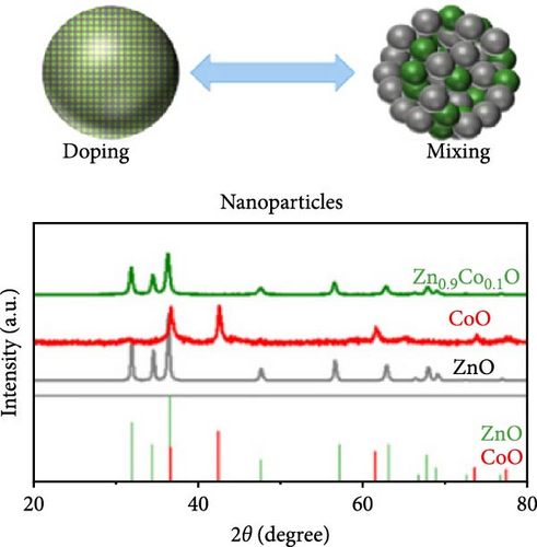
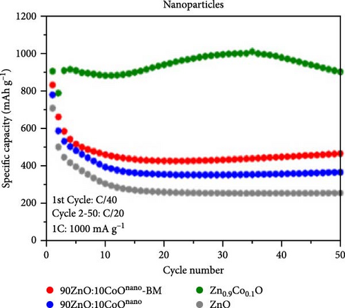
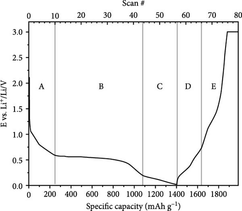
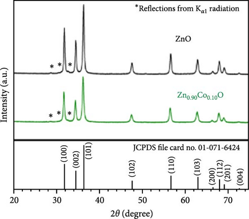
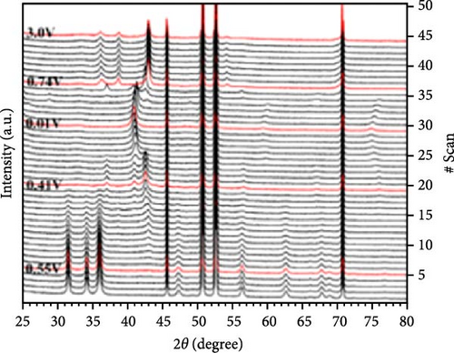
To address the challenges of poor performance and rapid capacity decay of ZnO as an anode material for LIBs, researchers have investigated Co-doped ZnO materials synthesized by different processes. Co-doped ZnO nanoparticles were synthesized via an aqueous solution method, followed by heat treatment and calcination. XRD confirmed a hexagonal wurtzite structure and successful Co doping. In situ XRD revealed that Co doping enhanced ZnO cycling stability by facilitating LixZn formation, suppressing zinc grain growth, and promoting reversible Li2O degradation during lithiation/delithiation (Figure 7a–c) [97]. Similarly, Co-doped ZnO was synthesized using a sol–gel method, with XRD analysis confirming successful Co incorporation up to 0.09 without the formation of secondary phases. In-situ XRD revealed Zn0.91Co0.09O lithiation/delithiation involved reduction, Li alloying, particle fragmentation, and partial regeneration with low crystallinity (Figure 7d–f) [98]. In another work, Zn0.9Co0.1O nanomaterials were synthesized using solution evaporation and calcination methods, with XRD analysis confirming the retention of the hexagonal wurtzite structure (Figure 7g) [99]. In-situ XRD confirmed that Co doping enhances lithiation mechanisms through reduction and alloying processes, thereby significantly improving the electrochemical performance of ZnO-based anodes (Figure 7h,i).
Details are in the caption following the image
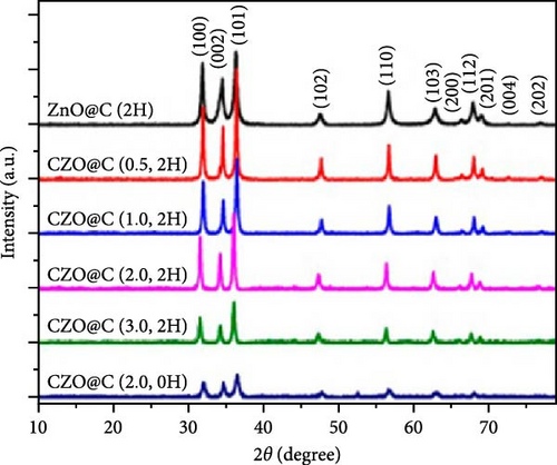
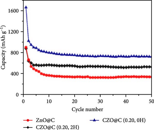
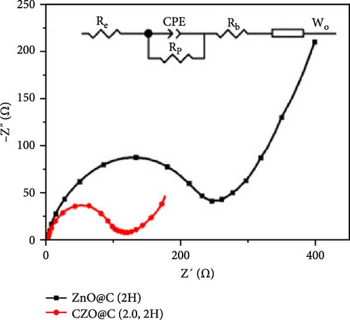
(a) XRD patterns of ZnO nanoparticles, (b) in situ XRD analysis of ZnO, (c) Zn0.9Co0.1O, reproduced with permission from [97], (d) XRD patterns of Zn1−xCoxO, (e) in situ XRD scans, (f) presented in 3D form, reproduced with permission from [98], (g) schematic illustration and XRD patterns of the Co-doped ZnO and the ZnO/CoO composites, (h) specific capacity for the nanosized materials/composite, (i) the dis/charge curve separated in five different regions, reproduced with permission from [99]; (j) XRD patterns, (k) cycling performances, and (l) EIS of ZnO@C and CZO@C products, reproduced with permission from [100].

Doping ZnO with carbon materials can alleviate volume expansion and enhance conductivity in electrode materials. Co-doped ZnO nanomaterials were modified using metal-organic frameworks (MOFs) as the carbon source to produce CZO@C composites [100]. XRD patterns revealed a shift in diffraction peaks to higher angles after Co doping, indicating lattice contraction due to Co ion incorporation (Figure 7j). Electrochemical tests showed that CZO@C maintained a high capacity (725 mAh g−1) after 50 cycles, significantly outperforming undoped ZnO@C (335 mAh g−1), with less capacity decay and better cycling stability (Figure 7k–l). These results indicate that carbon coating effectively mitigates volume expansion during charge/discharge, enhancing conductivity and structural stability, thereby significantly improving electrochemical performance [47, 87].

5. Fe Doped ZnO Nanoparticles

5.1. Application in Supercapacitors

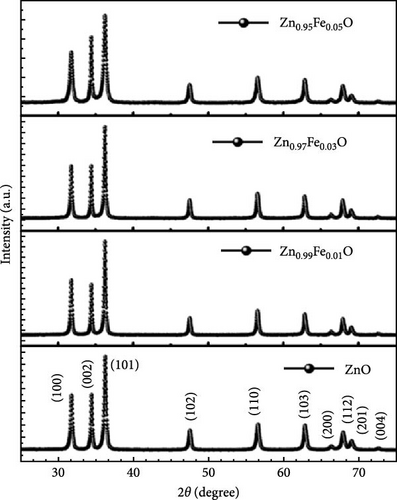
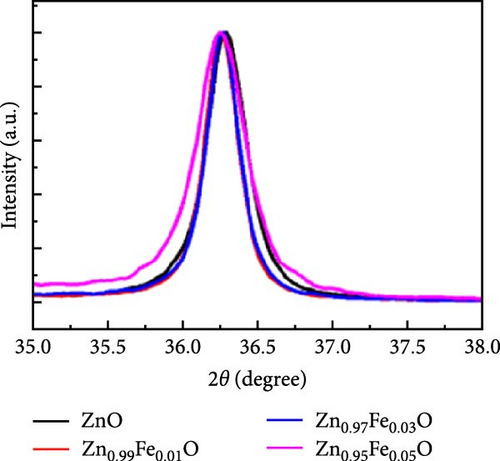
Fe doping affects the energy storage performance of ZnO nanostructures through multiple ways. Fe-doped ZnO nanostructures with varying Fe concentrations (1%–5%) were synthesized using a microwave irradiation method, demonstrating potential as supercapacitor electrode materials. XRD patterns showed a wurtzite structure for all samples, with no impurity peaks, eliminating the possibility of secondary phases (Figure 8a,b) [101]. As Fe doping increased, the diffraction peaks shifted to lower 2θ values, indicating lattice parameter expansion (a and c) due to lattice distortion [103]. Electrochemical tests showed that 3% Fe-doped ZnO electrodes exhibited a high specific capacitance of 286 F g−1 at a scan rate of 10 mV s−1 (Figure 8c), with a capacitance retention rate of 85% after 2000 cycles, demonstrating excellent cycling stability. However, this enhancement is not linear across doping concentrations. As Fe content increases beyond 3%, a decline in performance is observed due to excessive defect generation, which disrupts charge transport pathways and induces electrochemical instability.
Details are in the caption following the image
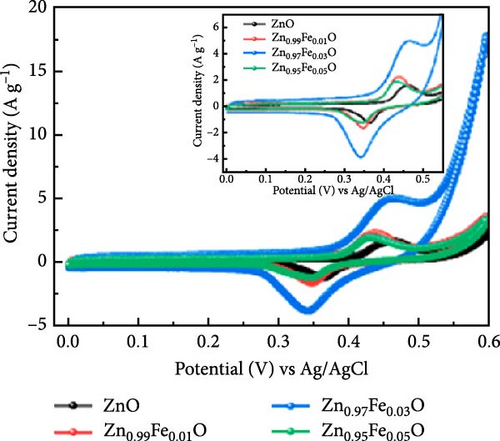
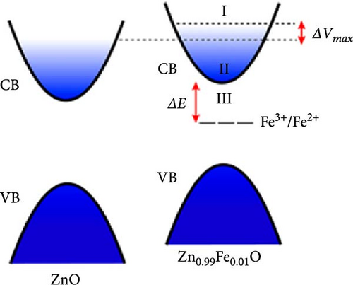
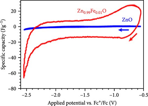
(a) XRD patterns of pure ZnO and Fe-doped ZnO nanostructures, (b) magnified view showing the shift of high-intensity towards lower 2θ values, (c) CV curves of Fe-doped ZnO nanostructures at 10 mV·s−1, reproduced with permission from [101], (d) differences in the electronic structures between ZnO and Zn1−xFexO nanocrystals, and (e) CV curves of drop-cast Zn0.99Fe0.01O and ZnO nanocrystals in a three-electrode cell, reproduced with permission from [102].

Doping Fe into ZnO nanocrystals can effectively enhance the charge storage capability of the corresponding electrodes. Fe-doped ZnO (Zn0.99Fe0.01O) nanocrystals with an average particle size of 8.7 nm were synthesized using a photodoping method [102]. The Zn0.99Fe0.01O nanocrystals exhibited an area capacitance of 33 μF cm−2 and a volumetric capacitance of 233 F cm−3, much higher than activated carbon (5–15 μF cm−2) [104] as well as advanced electrodes based on graphene (include values) [105] and MOFs [106]. The capacitance improvement is attributed to intermediate Fe (3d) orbitals within the nanocrystals, which store additional electrons. Fe doping not only enhances capacitance but also increases electron storage at low potentials, demonstrating potential for high-capacitance energy storage devices (Figure 8d,e).

5.2. Application in Lithium Batteries

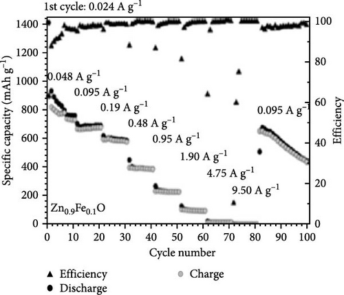
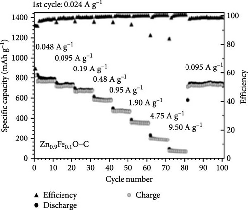
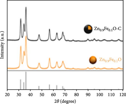
Fe-doped ZnO nanoparticles demonstrate outstanding electrochemical performance as anode materials for LIBs. Fe-doped ZnO nanoparticles (Zn0.9Fe0.1O) were synthesized using a sucrose-assisted wet chemical method, with performance further improved through a carbon coating [107]. XRD results confirmed that the doped and carbon-coated ZnO maintained a hexagonal wurtzite structure with no secondary phases (Figure 9a). The Zn0.9Fe0.1O material showed an initial reversible capacity of ~900 mAh g−1, but experienced significant capacity fading and poor cycling stability. In contrast, the carbon-coated Zn0.9Fe0.1O─C material exhibited a slightly reduced initial capacity of about 840 mAh g−1 but maintained a high capacity of ∼800 mAh g−1 in subsequent cycles (Figure 9b–d). The phase transitions and structural changes of Zn0.9Fe0.1O electrodes during lithiation and delithiation were further examined using operando XRD. Analysis of the XRD patterns revealed four distinct regions in the lithiation process (Figure 9e) [108].
Details are in the caption following the image
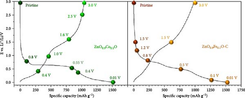
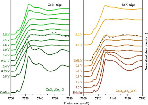
(a) XRD patterns of Fe-doped ZnO and cycle performance of different electrodes, (b) ZnO, (c) Zn0.9Fe0.1O, (d) Zn0.9Fe0.1O─C, reproduced with permission from [107], (e) schematic illustration of the initial lithiation mechanism and operando XRD analysis of Zn0.9Fe0.1O─C electrodes, reproduced with permission from [108], (f) first cycle dis/charge profiles of Zn0.9Co0.1O and Zn0.9Fe0.1O─C electrodes, and (g) ex situ XANES spectra at Co K-edge and Fe K-edge for electrodes derived from Zn0.9Co0.1O and Zn0.9Fe0.1O─C, reproduced with permission from [109].

X-ray absorption spectroscopy (XAS) revealed that the valence state of doped metals plays a crucial role in determining the electrochemical reaction mechanism [109, 110]. Fe-doped ZnO (Zn0.9Fe0.1O) and Co-doped ZnO (Zn0.9Co0.1O) exhibit different mechanisms during lithiation. The Co-doped ZnO lattice retains local stability similar to the wurtzite structure, with cobalt reduction occurring at lower potentials, forming a stable Co–Zn alloy [111]. In contrast, during the initial lithiation of Zn0.9Fe0.1O, Fe3+ is first reduced to Fe2+ and then to metallic Fe, with the resulting Fe nanoparticles acting as nucleation sites for Zn reduction and FexZn alloy formation. During delithiation, Fe gradually reoxidizes but to a limited extent. On the other hand, Zn0.9Fe0.1O exhibits superior initial capacities but faster capacity fading compared to Zn0.9Co0.1O, attributed to Fe-induced electrolyte decomposition and excessive LiF formation [110]. These findings are crucial for understanding the impact of metal doping on the electrochemical performance of ZnO materials (Figure 9f,g).

6. Mn-Doped ZnO Nanoparticles

6.1. Application in Supercapacitors

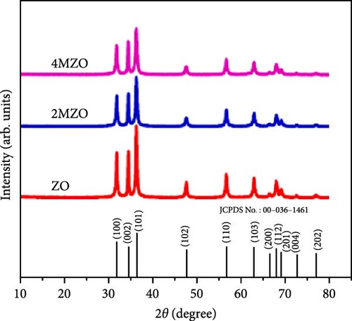
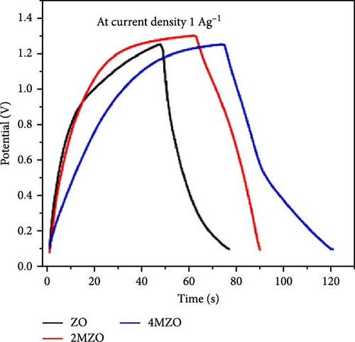
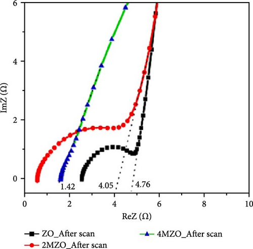
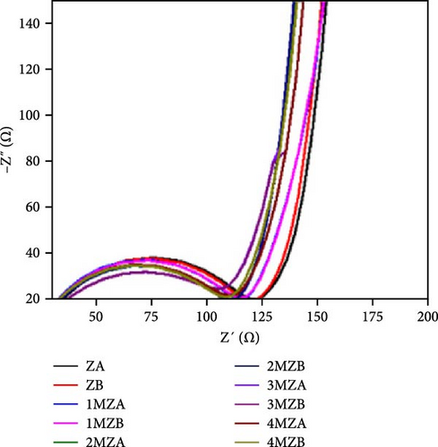
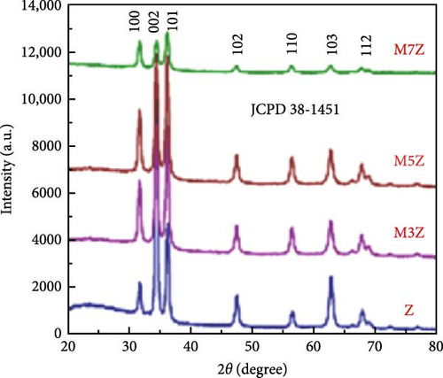
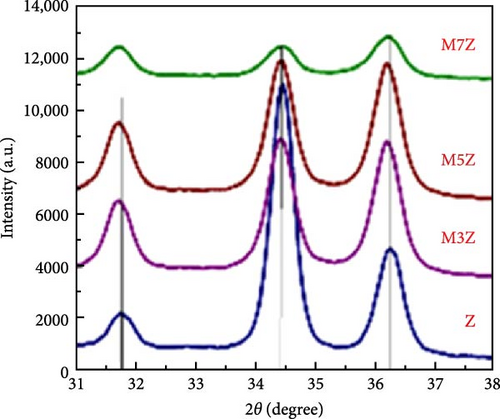
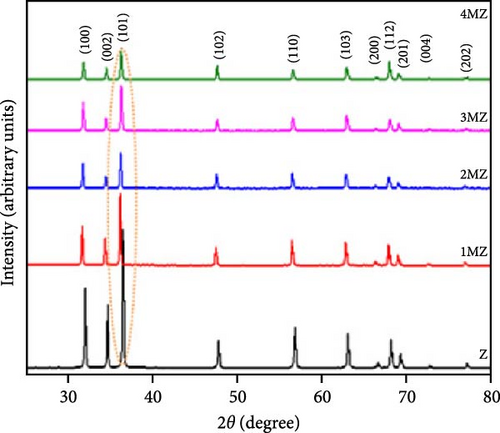
Manganese (Mn) doping improves the crystal structure and electrical conductivity properties of ZnO, enhancing its stability and suitability for energy storage applications [43, 112, 113]. ZnO and Mn-doped ZnO thin films with varying Mn concentrations were synthesized via a spray pyrolysis method for supercapacitor applications [114]. XRD analysis confirmed the presence of hexagonal wurtzite ZnO structures in all samples, with no evidence of manganese oxides or other phases (Figure 10a). Mn doping shifted diffraction peaks to lower angles, indicating lattice expansion due to the substitution of larger Mn2+ ion for Zn2+, and caused a linear increase in the c-axis lattice constant (Figure 10b). Electrochemical studies revealed significant pseudocapacitive behavior in Mn-doped ZnO films, characterized by improved ion intercalation/deintercalation and reduced internal resistance (Figure 10c). Similarly, ZnO doped with 2 and 4 wt% Mn, synthesized via sol–gel and co-precipitation methods, exhibited grain size reductions from 26.25 to 20.26 nm (Figure 10d) [115]. These films demonstrated enhanced capacitance (164.28 F g−1 for 4% Mn vs. 42.83 F g−1 for undoped ZnO), reduced internal resistance, and improved reaction kinetics (Figure 10e,f). These findings underscore the potential of Mn-doped ZnO as a high-performance electrode material for energy storage.
Details are in the caption following the image
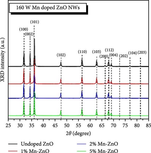
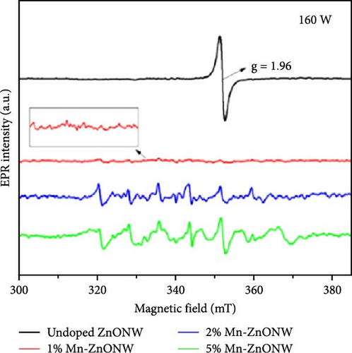
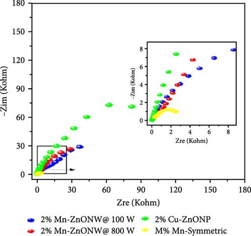
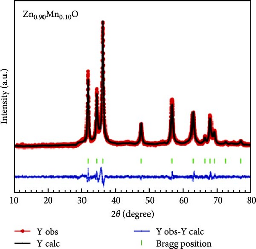
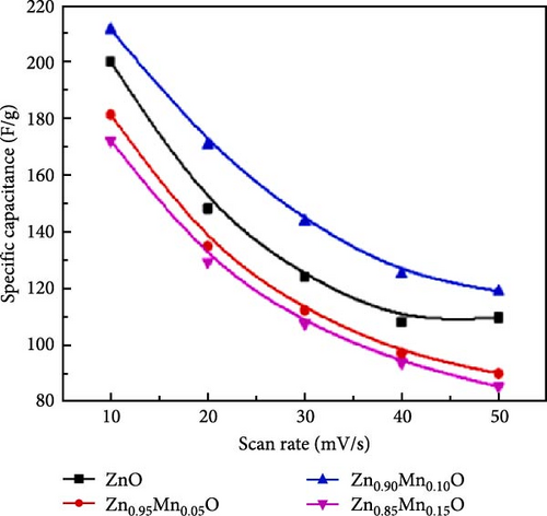
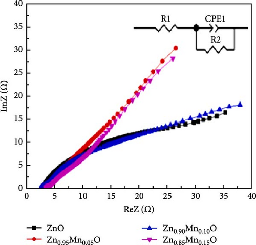
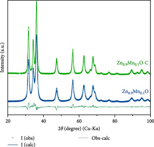
(a) XRD pattern, (b) XRD peak shift of pure ZnO and Mn-doped ZnO thin films, (c) CV curves of Mn-doped ZnO thin films at 10 mV s−1 scan rate, reproduced with permission from [114], (d) XRD patterns, (e) GCD plots at 1 A g−1, (f) Nyquist plot for ZO, 2MZO, and 4MZO samples, reproduced with permission from [115], (g) XRD patterns, (h) EPR spectra of Mn-doped ZnO NWs at 1%, 2%, and 5% doping concentration, (i) corresponding EIS, reproduced with permission from [112], (j) experimental and Rietveld refined XRD spectras of the Zn0.9Mn0.1O electrodes, (k) CV-derived specific capacitance vs. scan rate, and (l) EIS spectra along with its equivalent circuit for different electrodes, reproduced with permission from [116].

The introduction of Mn increased the defect density in the ZnO lattice, which acted as active sites to enhance electrochemical activity [34, 37]. Mn-doped ZnO materials were synthesized using the hydrothermal method, with XRD analysis confirming the wurtzite structure and successful incorporation of Mn2+ into the ZnO lattice (Figure 10g) [112]. Electron paramagnetic resonance (EPR) analysis revealed a significant increase in external defects due to doping, further boosting electrochemical performance (Figure 10h). Electrochemical tests showed that 2% Mn-doped ZnO nanowires exhibited a specific capacitance of 151 F g−1, attributed to the defects introduced by doping and the reduced charge transfer impedance (Figure 10i). However, the correlation between defect density and crystallite size was not thoroughly quantified.

Precise control of Mn doping concentration is crucial for optimizing the capacitance performance of ZnO nanomaterials. Excessive Mn doping introduces more lattice defects and dislocations, reducing conductivity and electrochemical performance [117, 118]. Zn1−xMnxO (x = 0–0.15) nanomaterials and thin films were synthesized using the sol–gel method and studied for supercapacitor applications [116]. XRD analysis confirmed a hexagonal wurtzite structure with no secondary phases (Figure 10j). As Mn concentration increased, the average grain size decreased, while lattice strain and dislocation density increased. Electrochemical tests showed specific capacitance values of 200 F g−1 for undoped ZnO and 185, 220, and 172 F g−1 for ZnO with Mn concentrations of 0.05, 0.10, and 0.15, respectively (Figure 10k). Electrochemical impedance spectroscopy (EIS) analysis indicated the lowest charge transfer resistance at x = 0.10, highlighting efficient charge transfer (Figure 10l). Thus, optimal Mn doping (x = 0.10) significantly enhances the capacitance performance of ZnO nanomaterials, while excessive doping introduces defects and reduces performance.

Significant discrepancies remain among studies regarding the optimal doping concentration. For example, Ammar et al. [112] suggested an optimal range of 1%–2%, while Rana et al. [116] identified 10% as the ideal concentration. Moreover, the role of impurity phases in electrochemical activity has yet to be clearly elucidated. Future research should focus on establishing standardized synthesis and testing protocols, as well as exploring the integration of hybrid materials to further enhance performance.

6.2. Application in Lithium Batteries

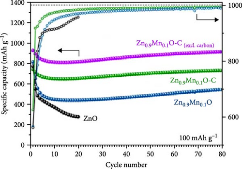
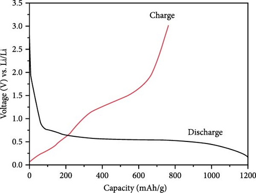
Mn doping provides additional active sites, significantly enhancing the energy storage performance of ZnO electrodes in LIBs [119]. Porous Zn1−xMnxO nanosheets were synthesized using a high-temperature calcination method, with XRD analysis confirming their hexagonal wurtzite structure (Figure 11a) [120]. The Zn0.8Mn0.2O porous nanosheets exhibited an initial discharge and charge capacity of 1198 and 763 mAh g−1, respectively, and maintained a stable capacity of 210 mAh g−1 after 300 cycles (Figure 11b,c). In another work, Zn0.9Mn0.1O and Zn0.9Mn0.1O─C materials were prepared through a pyrolysis-calcination process (Figure 11d) [119]. Rietveld XRD refinement indicated that Mn doping caused lattice expansion, while the carbon coating significantly improved crystallinity (Figure 11e). Real-time monitoring of structural changes during electrochemical cycling revealed that the carbon coating partially reduced and repositioned Mn in the lattice. Electrochemical tests showed that Zn0.9Mn0.1O─C exhibited higher reversibility, better coulombic efficiency, superior rate performance, and longer cycle life, demonstrating the carbon coating’s role in promoting MnZnx alloy formation during lithiation (Figure 11f).

Details are in the caption following the image
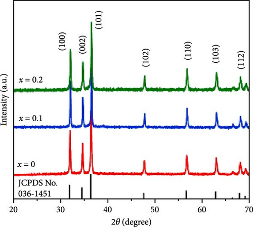
(a) XRD patterns of ZnO and Mn-doped ZnO samples, (b) initial dis/charge curve for Zn0.8Mn0.2O, (c) cycle performances and Coulombic efficiencies of different electrodes, reproduced with permission from [120], (d) illustration of the preparation process of Zn0.9Mn0.1O, (e) XRD patterns of Zn0.9Mn0.1O and Zn0.9Mn0.1O─C, (f) specific capacity stability for different electrodes, reproduced with permission from [119], (g) XRD patterns of ZnO and Zn1−xMnxO (x = 0.1, 0.2), (h) peak shift of (101) planes, and (i) rate performance of ZnO and Zn1−xMnxO, reproduced with permission from [121].

Sodium-ion batteries (SIBs) are considered a potential replacement for LIBs due to their similar working principles and the abundance and safety of sodium [122, 123]. Studies have shown that Mn doping significantly enhances the energy storage performance of ZnO in SIBs. Mn-doped ZnO nanoparticles (Zn1−xMnxO, 0 ≤ x ≤ 0.2) were synthesized via a co-precipitation method [121]. XRD results revealed that all samples maintained a wurtzite structure (Figure 11g). The doping caused a shift in the (101) plane peak positions, resulting in a slight increase in lattice parameters and a decrease in grain size (Figure 11h). A new MnO phase appeared at higher doping concentrations (x ≥ 0.3). Mn doping improved the rapid charge–discharge capability, with Zn0.8Mn0.2O reaching 239.9 mAh g−1 at 5 A g−1, whereas pure ZnO only achieved 99.9 mAh g−1 (Figure 11i). On the other hand, this work provides clear evidence of impurity phase formation at high doping levels, which limits structural integrity and performance.

Despite the ionic radius difference between Mn2+ (0.80 Å) and Zn2+ (0.74 Å), studies by Rana et al. [116] and Hussain et al. [121] consistently reported no formation of secondary phases within the 15%–20% Mn doping range, indicating a high compatibility of Mn2+ with the ZnO lattice. This compatibility is likely attributed to the effective substitution of Zn2+ by Mn2+, which induces limited lattice expansion without exceeding the strain tolerance of the ZnO lattice. Additionally, Mn doping introduces functional defects such as oxygen vacancies and zinc vacancies, while the strong interaction between Mn d-electrons and O2− contributes to lattice stability. However, doping concentrations exceeding 20% result in the precipitation of secondary phases, such as MnO, highlighting a doping saturation limit. This phenomenon expands the functionalization potential of ZnO for energy storage applications, emphasizing the need to explore the dynamic mechanisms of doping-induced defect and lattice deformation regulation.

7. Ni-Doped ZnO Nanoparticles

7.1. Crystal Structure Analysis of Ni-Doped ZnO

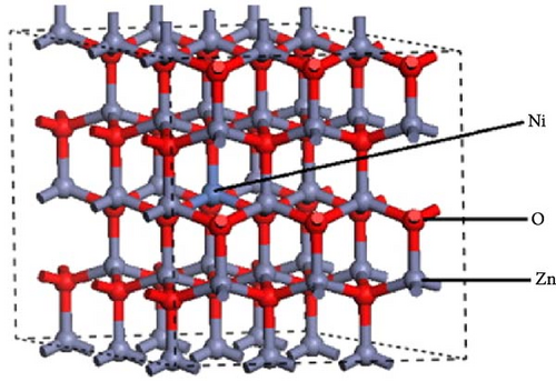
Ni doping effectively reduces the band gap energy between the valence and conduction bands due to its electron configuration of [Ar]3d84 s2. The two unpaired electrons in the 3d orbital enhance covalent bonding. Additionally, the ionic radius of Ni2+ (0.69 Å) closely matches that of Zn2+ (0.74 Å), facilitating efficient ion exchange. This substitution decreases the bandgap, forms new molecular orbitals, and introduces impurity energy levels in ZnO, thereby enhancing its performance [124, 125]. The supercell structure of Ni-doped ZnO with Ni2+ ions substituting Zn2+ ions in the lattice is illustrated (Figure 12a) [126]. This substitution results in localized lattice distortions, which are crucial for understanding the impact of Ni doping on the structural and electronic properties of corresponding materials.
Details are in the caption following the image
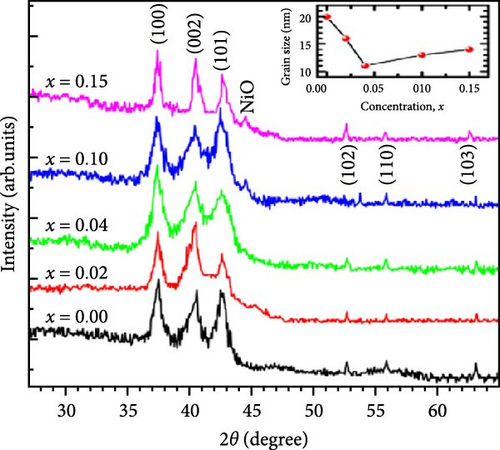
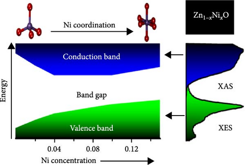
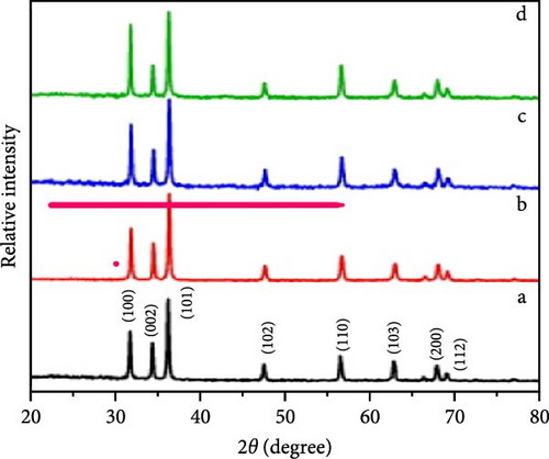
(a) Supercell structure of Ni doped ZnO, reproduced with permission from [126], (b) XRD patterns of ZnO and Ni (3%, 6%, 9%) doping ZnO, reproduced with permission from [127]; (c) XRD patterns, (d) W-H analysis of ZnO and Ni doping ZnO samples, reproduced with permission from [128], (e) XRD patterns for Zn1−xNixO films (the inset presents the calculated grain sizes derived from the XRD data), and (f) ZnO band gaps tuning mechanism with Ni doping, reproduced with permission from [129].

The grain size and lattice strain of Ni-doped ZnO nanoparticles are significantly affected by the doping concentration. Ni-doped ZnO nanorods (Zn1−xNixO, x = 0.0, 0.03, 0.06, and 0.09) were prepared through the co-precipitation process [127]. XRD analysis revealed major diffraction peaks corresponding to the hexagonal wurtzite structure (Figure 12b). The average particle size decreased from 37 to 31 nm with Ni doping up to 0.06 but increased to 39.1 nm at 0.09. The structural properties of Ni-doped ZnO at dilute concentrations were investigated, with samples synthesized using an organic co-precipitation method. XRD analysis confirmed a monophase hexagonal wurtzite structure with no secondary or impurity phases (Figure 12c) [128]. W–H analysis revealed consistent average particle sizes and confirmed the presence of microstrain (Figure 12d). The increase in crystallite size from W–H analysis, consistent with Scherrer equation and Vigard Law, is attributed to the movement of Zn interstitials to grain boundaries.

Ni doping significantly influences the band gap modulation of ZnO. The band gaps of pure and Ni-doped ZnO thin films, synthesized via spray pyrolysis deposition with Ni concentrations ranging from 0% to 15%, were systematically investigated. XRD patterns confirm the presence of a hexagonal wurtzite ZnO phase (Figure 12e) [129]. Ni doping significantly influences the band structure of ZnO by modulating the maximum of the valence band (VBmax) and the minimum of the conduction band (CBmin), enabling effective band gap tuning. At low doping concentrations, strong hybridization between Ni 3d states and O 2p states elevates the VBmax, while unoccupied Ni 3d states lower the CBmin, substantially reducing the band gap. With increasing doping concentration, changes in the symmetry of Ni 3d states slow the rise of VBmax, and CBmin begins to increase (Figure 12f). Another study reported that the energy bandgap ranges from 3.55 to 3.71 eV, depending on the Ni dopant concentration [130]. These findings highlight the potential of Ni doping to optimize ZnO band gaps for diverse applications.

The density functional theory (DFT) plays a crucial role in tuning the bandgap and can predict both the magnitude and nature of the bandgap in semiconductor materials. Many studies have shown that the energy band gap (Eg) of pure ZnO and TM-doped ZnO is severely underestimated by experimental findings, with the bandgap tending to decrease upon TM doping. This discrepancy stems from the underestimation of d-state binding energy by the generalized gradient approximation (GGA) approach [131, 132]. Previous reports indicated that while the inclusion of the Hubbard correction for Ud,Zn and/or Ud,TM slightly improved the calculated Eg, it remains underestimated experimentally. However, incorporating Up,O significantly enhanced the accuracy of the calculated Eg. Furthermore, TM doping induced localized density peaks in the minority spin states [133]. In pure ZnO, increased electronic overlap in Zn─O bonds weakens covalent interactions, whereas TM doping modifies the overlap in TM─O and Zn─O bonds. More electronegative TMs enhance ionic character, while less electronegative TMs increase covalency [134].

7.2. Application in Supercapacitors

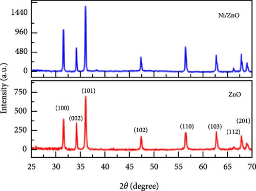
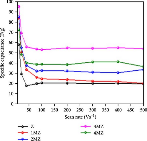
Ni doping not only enhances the specific capacitance of ZnO electrodes but also significantly improves their charge transfer performance and electrochemical stability, demonstrating superior energy storage capabilities in supercapacitor applications. Ni-doped ZnO materials with Ni concentrations of 0.0%, 0.5%, 1%, 1.5%, and 2% were synthesized using a high-energy ball milling method. XRD analysis confirmed that all samples exhibited a hexagonal wurtzite crystal structure, with no secondary peaks related to Ni or impurities (Figure 13a) [42]. Ni doping improved the electrochemical performance of ZnO electrodes, with the highest specific capacitance of 95.32 F g−1 at 1.5% Ni doping, significantly higher than undoped ZnO (Figure 13b). EIS revealed a reduced charge transfer resistance in Ni-doped samples (Figure 13c), indicating enhanced charge transfer efficiency, improved electrochemical stability, and higher coulombic efficiency. Consistent findings from other studies further validate that Ni doping effectively minimizes charge transfer resistance [38, 137].
Details are in the caption following the image
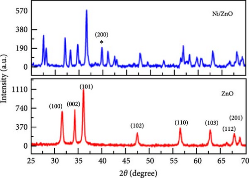
(a) XRD patterns of ZnO and Ni doped ZnO structures, (b) specific capacitance at different scan rates, (c) Nyquist plots before and after CV cycle tests, reproduced with permission from [42], XRD patterns of pure and Ni doped ZnO nanoparticles synthesized by (d) co-recipitation, (e) hydrothermal methods, (f) charge–discharge curves of Ni doped ZnO prepared by hydrothermal methods, reproduced with permission from [135], (g) XRD patterns of ZnO and Ni doped ZnO nanoflowers, (h) specific capacitance vs. current density obtained from GCD, and (i) EIS of different samples, reproduced with permission from [136].

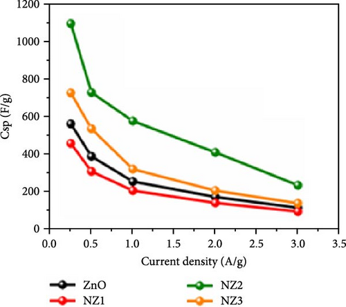
Incorporating Ni into ZnO effectively regulates intrinsic defects, such as zinc interstitials and oxygen vacancies, which play a critical role in determining electrical and magnetic properties. Ni/ZnO nanomaterials were synthesized using co-precipitation and hydrothermal methods to compare their structural and electrochemical performance. Co-precipitated samples exhibited an additional peak at 43.29°, indicating the presence of a NiO phase, whereas hydrothermally synthesized samples displayed no impurity peaks (Figure 13d,e) [135]. Electrochemical analysis revealed Faradaic redox peaks in hydrothermally prepared samples, signifying high capacitance and excellent reversibility (Figure 13f). Similarly, Ni-doped ZnO nanoflowers with varying doping levels (3%, 5%, and 7%) were synthesized using hydrothermal methods. XRD patterns showed no secondary phases but a slight reduction in diffraction peak intensity (Figure 13g) [136]. The Ni-doped ZnO nanoflowers achieved a remarkable specific capacitance of 1090 F g−1 at 0.25 A g−1, significantly surpassing undoped ZnO (Figure 13h). EIS measurements further confirmed reduced charge transfer resistance (Rct), enhanced conductivity, and improved charge transfer efficiency (Figure 13i).

The above studies indicate that crystallite size and defect concentration vary significantly depending on synthesis methods and doping levels, which in turn impact electrochemical performance. Notably, research on Ni-doped ZnO nanoflowers reported a specific capacitance of 1090 F g−1, substantially surpassing the values observed in other investigations on similar materials [136]. This disparity is likely attributed to the unique chrysanthemum-like morphology, which effectively maximizes active sites and electron transport pathways. Future research should focus on tailoring material morphologies through precise synthesis techniques to optimize specific surface area and defect distribution, thereby further enhancing electrochemical performance.

8. Other Metal Ions Doped ZnO Nanomaterials Applicated in Energy Storage Systems (Cu/Cr/Al/Mo/V/Nd/Ca/Ag)

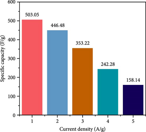
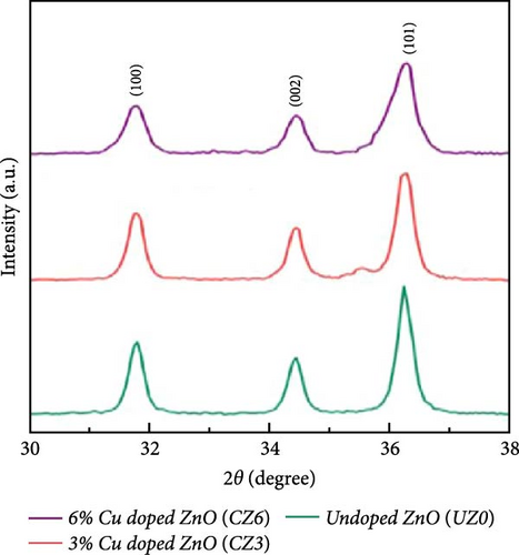
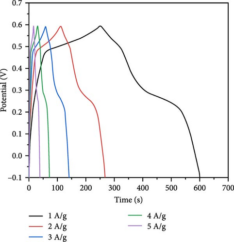
In electrochemical applications, Cu doping not only reduces ZnO grain size and increases specific surface area and active sites but also enhances electrical conductivity due to the excellent conductive properties of Cu ions [138, 139]. Cu-doped ZnO nanoparticles with Cu doping levels ranging from 0 to 6 wt% were prepared using the co-precipitation technique [29]. XRD analysis verified that all samples exhibited a hexagonal wurtzite ZnO structure, with no additional peaks associated with copper oxide (Figure 14a). Increasing Cu concentration from 0 to 6 wt% resulted in a decrease in average crystallite size from 25.87 to 22.51 nm. The Zn0.94Cu0.06O electrode achieved a maximum specific capacitance of 503.03 F g−1 at 1 A g−1, attributed to its increased surface area and reduced crystallite size (Figure 14b,c). Additionally, Zn0.98Cu0.02O/PVDF composites demonstrated improved energy storage properties, as Cu ion doping introduced lattice distortions, increased dipole moments, and enhanced polarization capacity [142]. These advancements provide novel insights for designing high-performance energy storage materials with potential applications in smart wearable devices.
Details are in the caption following the image
(a) XRD patterns of Cu doped ZnO samples, (b) GCD curve of Zn0.94Cu0.06O, (c) specific capacitance at various current densities, reproduced with permission from [29], (d) XRD patterns of Cr doped ZnO samples, (e) EPR spectra of the samples, (f) GCD plots of the electrodes at 1 A g−1, reproduced with permission from [140], (g) XRD patterns of Al doped ZnO nanowires, (h) specific capacitances at different current densities, and (i) EIS analysis of the ZnO and Al doped ZnO electrodes, reproduced with permission from [141].

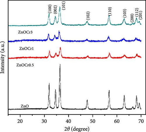
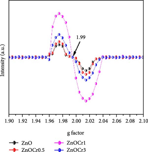
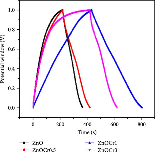
Chromium (Cr) doping in ZnO creates oxygen vacancies, which significantly enhance electron transport and electrolyte ion intercalation, thereby improving electrochemical performance. Cr-doped ZnO nanoparticles were synthesized using a simple sol–gel method, demonstrating potential for supercapacitor applications [140]. XRD patterns showed the typical hexagonal crystal structure of ZnO, with no impurity phases introduced by Cr doping (Figure 14d), consistent with the findings of Zhu et al. [143]. Combined with EPR analysis, these results confirmed the successful incorporation of Cr into the ZnO lattice and the generation of numerous oxygen vacancies (Figure 14e). The Zn0.99Cr0.01O electrode exhibited a high capacitance of 367 F g−1 (Figure 14f), maintaining 86% capacitance retention as current density varied from 1 to 20 A g−1, and 84% stability after 4000 cycles. Research indicates that the local spin interactions of Cr ions induce lattice distortion and generate defect energy levels, facilitating the formation of oxygen vacancies [144].

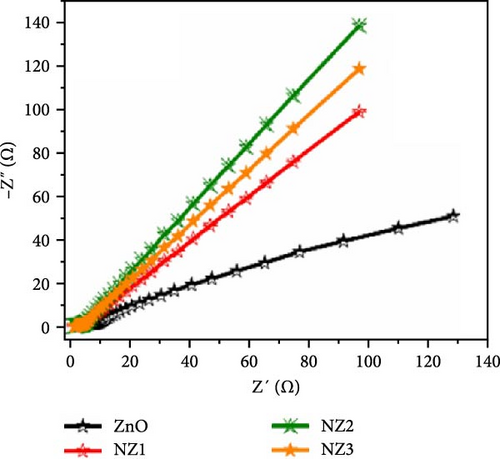
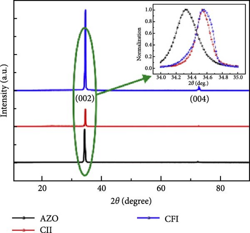
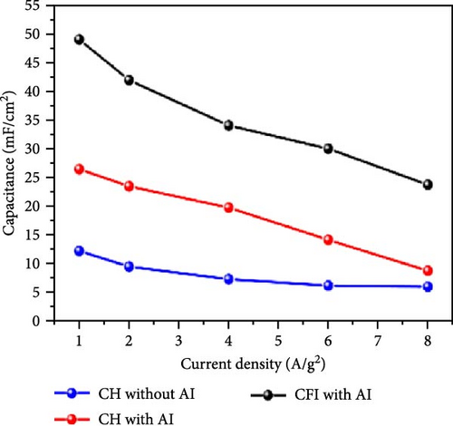
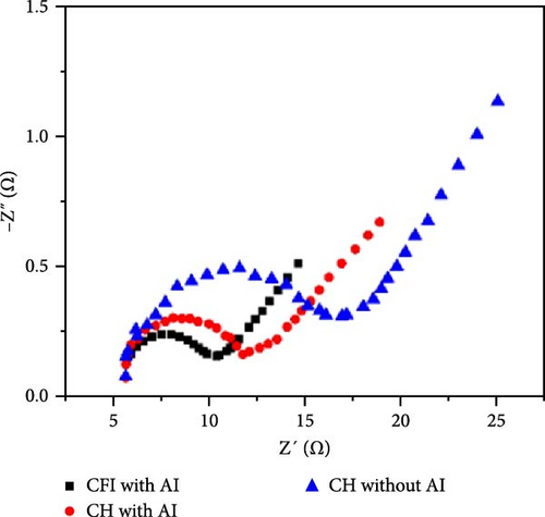
Al-doped ZnO nanowire arrays were synthesized in situ using a continuous flow injection (CFI) hydrothermal method, achieving a high carrier concentration. XRD patterns revealed a shift in the diffraction peaks of Al-doped ZnO relative to pure ZnO, confirming the absence of secondary phase formation (Figure 14g) [141]. This doping increased the carrier concentration from 1016 to 1019 cm−3, significantly enhancing conductivity (Figure 14h). EIS analysis showed a marked reduction in charge transfer resistance due to the excellent electron transport channels provided by the Al-doped ZnO nanowires (Figure 14i). Similarly, Al doping has been shown to introduce zinc and oxygen vacancies, optimizing the electronic structure of ZnO and greatly enhancing its potential for photocatalytic and electrochemical energy storage applications [145].

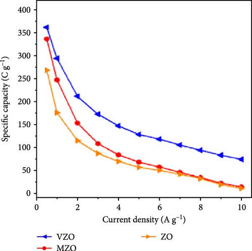
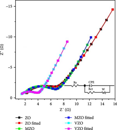
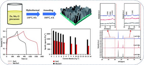
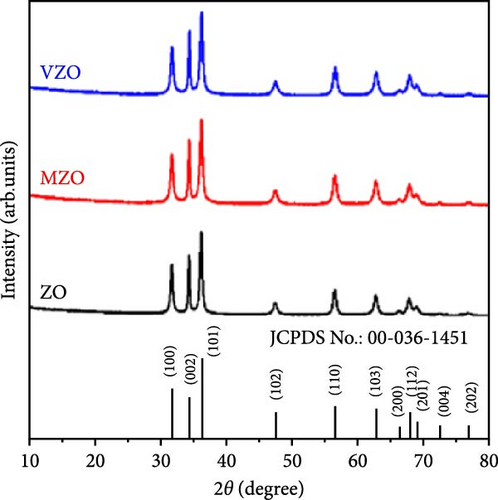
The study on Mo-doped ZnO nanosheets reveals that the introduction of Mo6+ ions (radius 0.59 Å) significantly enhances the conductivity, thereby improving its electrochemical performance as an electrode material. Mo-doped ZnO nanosheets were synthesized on Ni foam current collectors using a one-step hydrothermal method (Figure 15a) [146]. The prepared nanosheets exhibited excellent structural stability and cycle durability. Similar to Mo, vanadium (V) also possesses multiple valence states (+5, +4), providing multiple carriers that enhance conductivity and electrochemical active regions, thus improving the electrochemical performance of supercapacitors. Mo- and V-doped ZnO lotus-like structures were synthesized using a chemical co-precipitation method, and their performance in supercapacitor applications was systematically investigated. XRD showed that both undoped and doped ZnO samples exhibited hexagonal phase structures with high crystallinity (Figure 15b) [147]. Mo-doped ZnO (MZO) and V-doped ZnO (VZO) exhibited maximum specific capacities of 336 and 362 C g−1, respectively (Figure 15c). These excellent performances are due to the high crystallinity phase and lotus-like nanostructures provided by the doped elements (Figure 15d).
Details are in the caption following the image
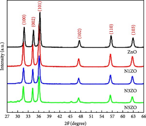
(a) Illustration of the synthesis process, electrochemical performance and XRD patterns of Mo doped ZnO nanoflakes, reproduced with permission from [146], (b) XRD patterns of ZnO, Mo doped ZnO, and V doped ZnO, (c) specific capacitances calculated from GCD profiles, (d) Nyquist plots, reproduced with permission from [147], (e) XRD patterns of ZnO and Nd doped ZnO nanoparticles, (f) GCD curves, and (g) Nyquist plots for ZnO and NZO nanoparticles, reproduced with permission from [148].

The rare earth metals possess the unique electronic structure, with electrons in their f-orbitals capable of various electronic transitions, significantly enhancing material conductivity [149]. ZnO nanoparticles doped with varying concentrations of Nd (Zn1−xNdxO) were synthesized using a microwave-assisted co-precipitation method. XRD results showed that samples doped with 1% and 3% Nd exhibited a typical wurtzite structure, with peak intensities decreasing as Nd concentration increased (Figure 15e) [148]. Electrochemical performance tests showed that the specific capacitance of undoped ZnO was 21 F g−1, while samples doped with 3% Nd reached 154 F g−1 (Figure 15f,g). Current research on rare-earth-doped ZnO primarily focuses on photocatalysis [150]. However, the introduction of rare-earth elements has been shown to significantly increase the concentration of oxygen vacancies on the ZnO surface and enhance its electron transport properties, providing crucial support for its potential applications in energy storage devices [151, 152].

Compared to single-ion doping, co-doping significantly enhances material conductivity and the number of active sites, optimizes the lattice structure, increases grain size, and improves internal stress, thereby enhancing the stability and electrochemical performance of electrode materials.

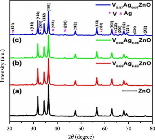
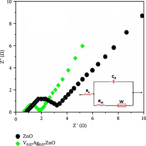
V─Ag co-doped ZnO nanorods were synthesized using a one-step sol–gel method. XRD testing showed that V and Ag doping significantly reduced the grain size of ZnO and decreased lattice parameters with increasing doping concentrations, indicating inhibited crystal growth and increased specific surface area (Figure 16a) [153]. The ZnO electrode doped with 7% V and Ag achieved a specific capacitance of 2700.19 F g−1 at a current density of 1 A g−1, compared to 402.1 F g−1 for undoped ZnO. After 5000 charge–discharge cycles, the electrode retained 93% of its specific capacitance, demonstrating excellent cycling stability. These improvements are due to the reduced grain size, increased specific surface area, and enhanced conductivity from co-doping (Figure 16b).
Details are in the caption following the image
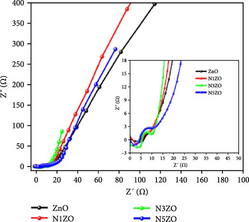
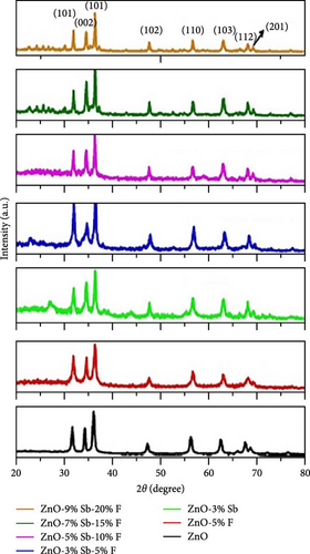
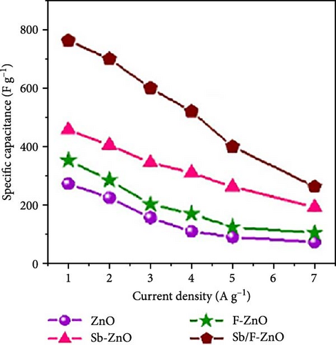
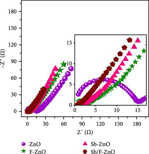
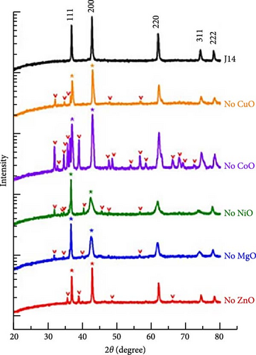
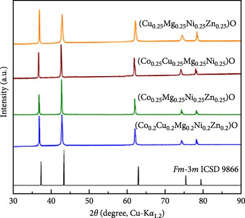
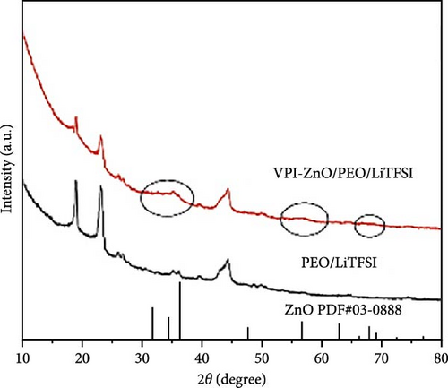
(a) XRD patterns of ZnO, V0.03Ag0.03ZnO, V0.05Ag0.05ZnO, and V0.07Ag0.07ZnO samples, (b) corresponding Nyquist plots, reproduced with permission from [153], (c) XRD patterns of nanostructures with various Sb/F doping levels, (d) Csp as a function of current densities for different electrodes, (e) Comparison of the Nyquist plots, reproduced with permission from [154], (f) XRD patterns for a composition series where individual components are removed, reproduced with permission from [155], (g) XRD patterns obtained during the first full de/lithiation cycle, reproduced with permission from [156], (h) XRD patterns of different samples with rock-salt structure, reproduced with permission from [157], and (i) GI-XRD patterns of PEO/LiTFSI and VPI-ZnO/PEO/LiTFSI, reproduced with permission from [158].

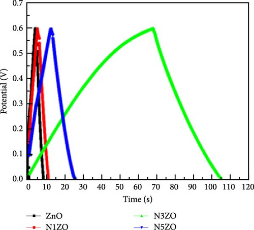
Antimony and fluorine co-doped ZnO (Sb/F-ZnO) nanoparticles were synthesized using the co-precipitation method. XRD peaks shifted toward higher angles and exhibited reduced intensity, indicating a decrease in crystallinity and the introduction of compressive stress within the lattice (Figure 16c) [154]. Electrochemical performance tests showed that the Sb/F-ZnO material achieved a specific capacitance of 762 F g−1 at a current density of 1 A g−1, significantly higher than that of the undoped sample (Figure 16d). These results demonstrate the synergistic effect of Sb and F co-doping, effectively tuning the ZnO crystal structure and improving its electronic conductivity and energy storage performance (Figure 16e).

Various types of dual-ion doping in ZnO have been reported. Capsule-shaped Ca─Co co-doped ZnO (Ca─Co@ZnO) materials were synthesized using a one-step hydrothermal method. XRD analysis revealed that Ca and Co induced orientation changes and lattice strain in the ZnO structure, leading to reduced XRD peak intensity and increased grain size. The Ca─Co@ZnO material exhibited a high specific capacitance of 1020 F g−1, which is 3.2, 1.7, and 1.6 times higher than that of pure ZnO, Ca─ZnO, and Co─ZnO, respectively [159]. In ZnO nanoparticles co-doped with Cu and Ni, prepared using the co-precipitation method, the XRD peak intensity decreased with increasing Cu and Ni concentrations, significantly reducing the average grain size while increasing dislocation density and microstrain. The Zn0.92Cu0.02Ni0.06O electrode demonstrated a specific capacitance of 596.43 F g−1 at a scan rate of 10 mV s−1, which was significantly higher than the 379.78 F g−1 of the pure ZnO electrode, with a capacity retention rate of ∼94% after 2000 cycles [160].

Mg─Ni co-doping [137] and Cd─Co co-doping [36] in ZnO have been studied for supercapacitor applications due to their unique electrical and magnetic properties, significantly enhancing electrode energy storage capacity. The doping elements improved ZnO conductivity and the number of active sites, optimized the lattice structure, increased grain size, and improved internal stress, making the electrode materials more stable during electrochemical reactions. SEM analysis indicated that doped ZnO nanoparticles had larger surface areas and uniform particle size distribution, increasing the active area of the electrodes and improving electrochemical reaction efficiency.

In recent years, high-entropy oxides (HEOs) have become a significant research focus in energy storage science and engineering due to their high disorder, excellent mechanical and thermal stability, electrochemical performance, and corrosion resistance. HEOs exhibit outstanding electrochemical performance in energy storage applications, particularly as electrode materials for LIBs, demonstrating high capacity and good cycling stability.

A HEO, (Co0.2Cu0.2Mg0.2Ni0.2Zn0.2)O, was prepared using the solid-state synthesis method. XRD analysis confirmed the single-phase structure of this kind of material (Figure 16f) [155]. Nanocrystalline HEOs, (Co0.2Cu0.2Mg0.2Ni0.2Zn0.2)O, were synthesized using the nebulized spray pyrolysis (NSP) method. Operando XRD was used to monitor real-time structural changes of HEO electrodes during the charge–discharge cycles of LIBs (Figure 16g) [156]. This technique revealed the evolution of the rock-salt structure of HEOs during lithium insertion and extraction, showing the positional changes of metal cations involved in the conversion reactions. In another study, XRD was used to comprehensively characterize the crystal phase structure of Co0.2Cu0.2Mg0.2Ni0.2Zn0.2)O materials and to analyze their structural changes during electrochemical cycling (Figure 16h) [157]. HEO materials demonstrate exceptional stability and conductivity during electrochemical reactions, mitigate volume changes in traditional metal oxides, lower production costs, and present broad application potential.

While XRD remains the gold standard for crystalline analysis of TMs-doped ZnO materials, its inherent limitations require complementary characterization methods. For example, intense proton irradiation can induce oxygen vacancy clustering through radiolysis effects, potentially influencing the intrinsic material properties [161]. Moreover, the “chemical state blindness” of XRD prevents the determination of oxidation states, which are critical for understanding energy storage mechanisms. These states can be precisely identified using X-ray photoelectron spectroscopy (XPS) through chemical shift analysis [142, 162164]. Raman spectroscopy also plays a crucial role in studying TMs-doped ZnO materials, such as Al-doped ZnO (AZO), by revealing structural features and defects. Complementary to XRD analysis, Raman spectroscopy is highly sensitive to the lattice defects and microstructural changes induced by doping [94, 145]. For instance, AZO samples exhibit strong peaks in their Raman spectra (e.g., the E1 (LO) mode at 574 cm−1 and the E2 (High) mode at 332 cm−1), which indicate the introduction of defects like oxygen/zinc vacancies [145]. These defects directly impact the catalytic and optoelectronic properties of the material.

In recent years, the rapid development of grazing incidence X-ray diffraction (GI-XRD) has provided critical support for studying the crystal structures of thin-film electrode materials and electrode–electrolyte interfaces. Compared with traditional XRD, GI-XRD employs a grazing incidence angle close to the critical angle, significantly enhancing its sensitivity to surface layers and thin-film structures. In the study of solid electrolytes based on a poly(ethylene oxide) (PEO) matrix modified with ZnO quantum dots, GI-XRD successfully detected the presence and distribution of ZnO quantum dots, which conventional XRD failed to identify (Figure 16i) [158]. Beyond providing high-resolution structural information, GI-XRD offers real-time in-situ monitoring capabilities, enabling the sensitive tracking of phase transitions in electrode materials and the formation of interfacial by-products [165, 166]. These capabilities are particularly valuable for studying failure mechanisms and dynamic performance. This emerging technology provides robust support for optimizing LIB materials and interfaces.

In recent years, significant progress has been made in the study of TMs-doped ZnO materials for supercapacitors and LIBs. The existing literature provides a comprehensive summary of various doping types, synthesis techniques, morphological characteristics, and electrochemical properties of ZnO materials developed over the past decade (Table 1).

Table 1. Summary of TMs-doped ZnO materials for supercapacitors and LIBs.
Materials Method/structure Electrochemical properties Highlights References
ZnO
  • • Hydrothermal method
  • • Hexagonal rod-like structure
• Specific capacitance of 5.87 F g−1 at 5 mV s−1 scan rate
  • • Zn (CH3COO)2, ZnCl2 and Zn (NO3)2 were used as precursors, respectively
  • • Influence of precursors on structure and properties was discussed
[14]
  
ZnO/ACNF
  • • Electrospinning method
  • • Nanofiber with average diameter of 200 ± 25 nm
• Symmetric cell with specific capacitance of 178.2 F g−1, 17.7 Wh kg−1 at 4 kW kg−1, 75% after 1000 cycles
  • • ZnO/ACNF were prepared using a one-step electrospinning technique combined with sol–gel processing
  • • The ZnO-CCNFs exhibit superior supercapacitor performance due to the well-distributed ZnO on ACNF and the optimized pore size distribution
[21]
  
ZnO/C
  • • Sol–gel method
  • • Spherical particle structure with size of 10–100 nm
  • • Half cell has the specific capacitance of 820 F g−1 at 1 A g−1
  • • Symmetric cell has 32.61 Wh kg−1 at 1 kW kg−1, 94% after 400 cycles
  • • Sucrose was used as caping agent and carbon source based on the green chemistry economy
  • • Carbon layer is helpful for the ion adsorption/desorption at the interface
[77]
  
Sandwich type ZnO/rGO/ZnO
  • • Sol-gel and dip-coating process
  • • Thickness of ZnO layers (~3 μm) and rGO paper (16 μm)
• Specific capacitance of 60.63 F g−1 at scan rate of 5 mV s−1
  • • Flexible ZnO/rGO/ZnO sandwich electrode is fabricated
  • • obviously improved capacitance compared with bare graphene
[78]
  
ZnO@CF
  • • Hydrothermal and calcination process
  • • ZnO nanoparticles encapsulated in a 3D hierarchical carbon framework, carbon layer with a thickness around 5 nm, the whole ZnO@C with a diameter around 30 nm
• Achieved a capacity of 850 mAh g−1 at a current density of 0.1 A g−1 after 200 cycles.
  • • 3D hierarchical carbon framework
  • • ZnO@CF demonstrates outstanding cycling stability and impressive rate capability
[83]
  
ZnO/Carbon nanofiber
  • • Electrospinning and subsequent thermal treatments
  • • ZnO/Carbon nanofibers of uniform diameters around 150 nm, with ZnO nanocrystals (about 10–30 nm)
• Delivered a capacity of 702 mAh g−1 at current density of 200 mA g−1 after 200 cycles
  • • Free-standing electrospun ZnO/Carbon nanofiber are constructed as anode
  • • 3D conductive network established
[85]
  
ZnO@graphene
  • • Precipitation and subsequent ball-milling process
  • • ZnO nanoparticles wrapped by graphene layers
• Full battery of ZnO@G || LiCoO2 delivered a reversible capacity around 400 mAh g−1 at 100 mA g−1 with working potential around 3.8 V
  • • ZnO–graphene composites were successfully synthesized using a sustainable and environmentally friendly approach
  • • The graphene layer establishes a 3D conductive network around ZnO nanoparticles, effectively mitigating their volume expansion during operation
  • • The properties of ZnO@graphene were evaluated in full batteries
[86]
  
ZnO/C
  • • One-step calcination
  • • Nanosized grains of ZnO covered with sheets-like carbon layer
• Capacity of 212 mAh g−1 at a high current rate of 100 mA g−1 after 100 cycles
  • • Nano/microscaled arrays of ZnO particles were synthesized by thermal treatment
  • • Ex situ XRD analysis reveals a two-step lithiation mechanism in ZnO, comprising a conversion reaction followed by an alloying process
[87]
  
Zn1−xCoxO
  • • Wet-precipitation method
  • • Quantum dot
  • • Half cell has the specific capacitance of 697 F g−1 at 1 A g−1
  • • Symmetric cell has 24 Wh kg−1 at 1026 W kg−1, 97% after 2000 cycles
  • • Doping resulted in more active sites and higher charge transfer efficiency
  • • Doing caused oxygen vacancies
[96]
  
ZnCoO
  • • Co-precipitation method
  • • Nanoparticles 7–10 nm
  • • Max doping content 20 at. % Co
  • • Half cell has the specific capacitance of 104.4 F g−1 at 1 A g−1
  • • Asymmetric ZnCoO//AC cell has 2.7 Wh kg−1 at 200 W kg−1, 98.1% after 4500 cycles
• Networking of Co-ions and hole polarons prevents structural damage [95]
  
Zn0.9Co0.1O
  • • Heat evaporation method
  • • Nanoparticles around 20–30 nm
• 789 mAh g−1 at a high current rate of 48 mA g−1 after 75 cycles
  • • Doping suppressed the zinc crystallite growth
  • • Beneficial impact on the reversible degradation of lithium oxide
[97]
  
Zn1−xCoxO (0 ≤ x ≤ 0.15)
  • • Sol-gel route
  • • Nanoparticles around 50 nm
• 600 mAh g−1 at a high current rate of 200 mA g−1 after 50 cycles • The effects of Co doping can be summarized as follows: stabilization of the Li2Zn phase, reduction in charge transfer resistance and improved reversibility of the reduction from metal oxide to metal [98]
  
CZO@C
  • • Calcination of MOF based materials
  • • Nanoparticles around 20 nm
• 725 mAh g−1 at a current rate of 100 mA g−1 after 50 cycles
  • • Co doping improved the conductivity of ZnO nanoparticles
  • • Doping also increased the degree of graphitization in the carbon
[100]
  
Zn0.97Fe0.03O (0.03 ≤ x ≤ 0.05)
  • • Microwave irradiation procedure
  • • Nanorod with diameter of 75 nm and length of 450 nm
• Half cell has the specific capacitance of 286 F g−1 at 10 mV s−1, 85% after 2000 cycles
  • • Bound magnetic polarons contribute to the ferromagnetic character of Fe doping samples
  • • The Fe-doped ZnO matrix exhibited a mixed valence state of Fe2+/Fe3+
[101]
  
Zn0.99Fe0.01O
  • • Precipitation and post-heating process
  • • Nanocrystals around 8.7 nm
• 233 F cm−3 at 10 mV s−1
  • • ‘Soluble supercapacitors’ was assembled by Zn0.99Fe0.01O nanocrystals
  • • Very high areal and volumetric capacitances
[102]
  
Zn0.9TM0.1O (TM = Fe or Co)
  • • Heat evaporated and post- calcination process
  • • Nanoparticles around 20 nm
  • • Zn0.9Fe0.1O: 800 mAh g−1 at a current rate of 48 mA g−1 after 30 cycles
  • • Zn0.9Co0.1O: 920 mAh g−1 at a current rate of 48 mA g−1 after 30 cycles
  • • In situ XRD analysis reveals the formation of LiZn alloy during the cycle process
  • • Synthesis process is simple and environmentally friendly
[107]
  
  • Mn-doped
  • ZnO (Mn: 3%, 5%, and 7%)
  • • Spray pyrolysis technique
  • • Thin film electrodes
• Half cell has the specific capacitance of 360 F g−1 at 10 mV s−1, 79% after 500 cycles • The electrodes were fabricated using a straightforward spray pyrolysis method [114]
  
Zn1−xMnxO (x = 0.03, 0.06)
  • • Co-precipitation method
  • • Nanoparticles around 30–50 nm
• Half cell has the specific capacitance of 324 F g−1 at 10 mV s−1 • Easy and eco-friendly synthesis method [37]
  
  • Mn-doped ZnO nanowires
  • (Mn: 1%, 2%, and 5%)
  • • Hydrothermal route
  • • Nanowires with an average length of 600 nm
• Asymmetric ZnMnO//MXene cell has the specific capacitance of 151 F g−1 at 100 mA g−1, 84 Wh kg−1 at 75 W kg−1, more than 95% after 50 cycles
  • • Presence of defects was verified via EPR and PL spectroscopy
  • • Impaction of defects on the performance of the supercapacitor was discussed
[112]
  
Zn1−xMnxO (x = 0–0.15)
  • • Sol–gel method
  • • Nanoparticles 20–40 nm
• Half cell has the specific capacitance of 220 F g−1, 2,202 W kg−1, and 1.15 Wh kg−1 • The band gap decreases with increasing Mn doping concentration [116]
  
Zn1−xMnxO (x = 0.1, 0.2, 0.44)
  • • Solvent precipitation method and post- calcination process
  • • Porous nanosheet
• 210 mAh·g−1 at a current rate of 120 mA g−1 up to 300 cycles
  • • Samples were fabricated using a cost-effective, scalable, and straightforward method
  • • The cavities between nanosheets effectively mitigate volume expansion
[120]
  
Zn0.9Mn0.1O/C
  • • Solution reaction and post-calcination process
  • • Nanoparticles around 20 nm
• 900 mAh g−1 at a current rate of 100 mA g−1 up to 80 cycles • Partial reduction of manganese after carbon coating, leading to the capacity improvement [119]
  
Zn1−xMnxO (0 ≤ x ≤ 0.2)
  • • Co-precipitation technique
  • • Nanoparticles around 30–50 nm
• 312 mAh g−1 at a current rate of 100 mA g−1 up to 200 cycles (93% retention rate)
  • • Fabricated through simple co-precipitation technique
  • • Various strategies have been employed to improve ion transport speed and enhance stability
[121]
  
  • Ni-doped ZnO
  • (0.0, 0.5, 1, 1.5, and 2 mol%)
  • • Ball-milling method
  • • Nanoplates around 500 nm
• Half cell has the specific capacitance of 96 F g−1 at 10 mV s−1, 97% after 5000 cycles • Internal resistance of the electrode was decreased after Ni doping [42]
  
Ni-doped ZnO
  • • Hydrothermal route
  • • Nanoflowers around 100–150 nm
• Half cell has the specific capacitance of 600 F g−1 at 1 A g−1, 101% after 8000 cycles • More active sites were formed after doping, which contributes to the capacity enhancement [136]
  
  • Cu-doped ZnO
  • (0–6 wt%)
  • • Co-precipitation method
  • • Nanoparticles around 22–25 nm
• Half cell has the specific capacitance of 503.03 F g−1 at 1 A g−1 • Cu has good capability to enhance the electrochemical performance of ZnO [29]
  
Cr-doped ZnO
  • • Sol–gel route
  • • Nanoparticles around 30 nm
  • • Half cell has the specific capacitance of 367 F g−1 at 1 A g−1
  • • Asymmetric ZnCrO//AC cell has 27.1 Wh kg−1 at 480 W kg−1, 83% after 4000 cycles
• The oxygen vacancies generation after doping contribute to the efficient electron transfer ability [140]
  
Al-doped ZnO
  • • Continuous flow injection method
  • • Nanowires with the height of 2.68 μm and the diameter are around 280 nm
• Half cell has the specific capacitance of 49 mF cm−2 at 1 mA cm−2
  • • The continuous flow injection is one of the simple and steady doping methods
  • • Al doping improved the conductivity of ZnO sample, which was further confirmed by first-principle theory
[141]
  
Mo-doped ZnO
  • • Single-step hydrothermal route
  • • Nanoflakes thickness of ~100 nm
  • • Half cell has the specific capacitance of 2,296 F g−1 at 1 A g−1
  • • Asymmetric ZnMoO//AC cell has 39 Wh kg−1 at 7.4 kW kg−1, 75.6% after 8000 cycles
• The electrochemical properties of ZnO were obviously enhanced by incorporating high capacity Mo ions [146]
  
V-doped ZnO
  • • Co-precipitation method
  • • Flower-like hierarchical structures ∼ 2 µm
  • • Half cell has the specific capacitance of 491 F g−1 at 1 A g−1
  • • Asymmetric ZnVO//AC cell has 32.4 Wh kg−1 at 5.16 kW kg−1, 85% after 2000 cycles
• The multiple valence states of V were helpful to enhance the electrical conductivity of ZnO [147]
  
Zn1−xNdxO (x = 0.00, 0.01, 0.03, and 0.05)
  • • Microwave assisted co-precipitation method
  • • Nanoparticles around 17–20 nm
  • • Half cell has the specific capacitance of 154 F g−1 at 2.5 A g−1
  • • Symmetric cell has 7.36 Wh kg−1 at 730 W kg−1, 92% after 1000 cycles
  • • Doing of Nd3+ in ZnO lattice is related to the generation of oxygen vacancies and other defects
  • • SXAS spectra is adopted to characterize the valence states of Zn and Nd, oxygen vacancies and defects
[148]
  
Ca─Co co-doped ZnO
  • • A single-step hydrothermal process
  • • Capsule-like structure with length of 87 nm
  • • Half cell has the specific capacitance of 1020 F g−1 at 0.75 A g−1, 92% after 5000 cycles
  • • Symmetric cell has 25.9 Wh kg−1 at 556 W kg−1
• Dual-ion doping enhances electron mobility, promotes efficient ion diffusion, and increases the number of active sites in the samples [159]
  
V-Ag co-doped ZnO
  • • One step sol–gel method
  • • Nanorods with length of 80 nm
• Half cell has the specific capacitance of 2714 F g−1 at 1 A g−1, 93% after 5000 cycles • The high electrochemical behavior in ZnO nanorods is due to the presence of V and Ag in the V0.07Ag0.07ZnO electrode [153]
  
Zn0.98–xCu0.02NixO (where x = 0.01, 0.03, 0.06)
  • • Chemical co-precipitation method
  • • Nano-spherical around 26 nm
• Half cell has the specific capacitance of 596 F g−1 at 10 mV s−1, 92% after 2000 cycles • The incorporation of Cu and Ni into the ZnO matrix enhances its photocatalytic activity and electrochemical performance [160]
  
Mg and Ni co-doped ZnO
  • • Sol–gel method
  • • Nanoparticles 35–70 nm
  • • Half cell has the specific capacitance of 750 F g−1 at 1 A g−1
  • • Symmetric cell has 93.7 Wh kg−1 at 3.76 kW kg−1, 95.2% after 5000 cycles
• Mg contributes to significant electrical properties, while Ni is utilized to enhance ferromagnetic behavior [137]
  
(Co0.2Cu0.2Mg0.2Ni0.2Zn0.2)O
  • • Nebulized spray pyrolysis method
  • • Hollow and filled spheres with sizes in the nano- to micrometer range
• 770 mAh g−1 at a current rate of 100 mA g−1 up to 100 cycles
  • • High entropy oxides exhibit substantial advantages in storage capacity and long cycling stability
  • • The performance of high-entropy oxides is influenced by the individual properties of the metal cations
[156]
  
(Mg0.2Co0.2Ni0.2Cu0.2Zn 0.2) O
  • • Nebulized spray pyrolysis method
  • • Nanoparticles around 2 μm
• 650 mAh g−1 at a current rate of 200 mA g−1 up to 40 cycles
  • • The ‘cocktail effect’ was explained by the multi-cations synergy effect during electrochemical reaction
  • • Elemental diversity plays a crucial role in optimizing multi-cation electrode materials
[157]

In order to better explore the application of ZnO materials in the practical energy storage market, the study compares ZnO with commercially used graphite and actively developed silicon–carbon composite materials (Figure 17a). The analysis indicates that ZnO offers distinct advantages in certain areas, making it a promising candidate for further investigation. ZnO materials are characterized by low production costs and excellent recyclability, particularly when using green processing techniques, with zinc recovery rates exceeding 90%. Compared to graphite, ZnO has a higher specific capacity, although its initial Coulombic efficiency is lower and it exhibits a relatively high volume expansion rate. ZnO also demonstrates longer cycling stability, especially after doping optimization, which enhances its electrochemical performance. In contrast, graphite remains the dominant anode material due to its low cost, mature production processes, excellent cycling stability, and high initial coulombic efficiency [167, 168]. Although silicon–carbon composites offer higher specific capacity, their large volume expansion and lower cycling life limit their practical application [169, 170]. Overall, ZnO shows clear advantages in terms of cost-effectiveness and environmental sustainability, making it well-suited for large-scale applications.
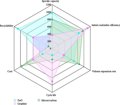
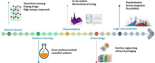
Details are in the caption following the image
(a) Comparison analysis of ZnO, graphite, and silicon/carbon composites; (b) Research roadmap of ZnO materials in the field of energy storage. ZnO, zinc oxide.
Details are in the caption following the image
(a) Comparison analysis of ZnO, graphite, and silicon/carbon composites; (b) Research roadmap of ZnO materials in the field of energy storage. ZnO, zinc oxide.

A research roadmap for ZnO materials in the field of energy storage has been included, covering the fundamental processes from material selection to large-scale production, with the aim of providing valuable assistance to the readers (Figure 17b). The process begins with material selection, focusing on theoretical screening of suitable dopants (such as Co, Fe, Mn, Ni, and Cu) and exploring dual- and multi-ion co-doping strategies to enhance performance. The next stage, synthesis technology, emphasizes the use of environmentally friendly, scalable synthesis methods that ensure consistent material quality and high performance. Following synthesis, characterization plays a critical role, involving advanced techniques such as in situ analysis and electrochemical testing to assess structural integrity, electrochemical behavior, and cycling performance of the material. In the subsequent phase, device design focuses on optimizing energy storage devices through the integration of ZnO-based composites, conductive polymers, and advanced packaging techniques to enhance stability and longevity. The final stage, large-scale production, prioritizes the adoption of green chemistry practices for sustainable manufacturing while optimizing production processes for industrial scalability.

9. Conclusion and Outlook

9.1. Conclusion

This paper systematically reviews recent research on TMs-doped ZnO in the fields of supercapacitors and LIBs, summarizing the following key points:

XRD analysis: XRD technology plays a critical role in studying TMs-doped ZnO materials. By precisely analyzing crystal structure, lattice parameters, grain size, and defect characteristics, XRD provides detailed insights into the impact of doping on the performance of ZnO-based materials. Moreover, in situ XRD enables real-time monitoring of structural changes, shedding light on energy storage mechanisms, electrode design optimization, and cycling performance. These findings are essential for tailoring the electrochemical properties of ZnO materials, ultimately enhancing their practical effectiveness in energy storage applications.

Lattice parameter changes: The lattice parameters of ZnO change significantly with the doping of different TMs, closely related to their ionic radii. Doping with larger ionic radius Mn2+ (0.80 Å) causes lattice expansion, while doping with smaller ionic radius Co2+ (0.72 Å), Fe3+ (0.63 Å), and Ni2+ (0.69 Å) leads to lattice contraction. Additionally, doping generally results in smaller grain sizes. Combined with suitable nanostructure design, this can reduce ion-electronic diffusion paths, which is crucial for improving material conductivity, increasing electrochemical active sites, and enhancing overall energy storage performance.

Band gap reduction: TM doping introduces additional d-orbital energy levels, reducing the energy required for electron transitions from the conduction band to the valence band, thus narrowing the band gap of ZnO materials. This modification enhances the conductivity and electrochemical activity of ZnO materials, significantly improving their performance in supercapacitors and LIBs.

Structural improvements: Doping with TMs introduces oxygen vacancies, lattice defects, and active sites, effectively mitigating mechanical stress and electrode material degradation caused by volume expansion. These improvements not only enhance the electrochemical performance of ZnO materials but also significantly extend their lifespan in energy storage systems. Future research can further optimize doping concentrations and methods to achieve higher performance and more stable energy storage materials.

9.2. Outlook

Looking ahead, the study of energy storage materials should extend from understanding intrinsic material properties to exploring multi-scale engineering applications.

Doping and nanostructure regulation have significantly enhanced the electrochemical performance of ZnO at the material level. However, substantial discrepancies remain among reported studies, indicating challenges in optimizing lattice parameters, defect concentrations, and surface morphologies to improve conductivity and mechanical stability. Advanced structural characterization techniques, such as in situ XRD, GI-XRD, and XAFS, are crucial for investigating the dynamic behavior of materials during cycling, offering insights into storage mechanisms. At the device design level, overcoming challenges like large-scale volume expansion and interfacial stability is key for ZnO-based supercapacitors and LIBs. Compositing ZnO with highly conductive materials, such as graphene or carbon nanotubes, can improve conductivity and structural stability, but further optimization is needed to enhance compatibility and energy density. At the engineering implementation level, transitioning from laboratory-scale synthesis to industrial-scale production is essential for the broader application of ZnO in energy storage devices. Green chemistry approaches can reduce costs and improve material uniformity, while interfacial regulation techniques, like constructing SEI layers, offer potential for enhancing cycle life and energy efficiency.

In summary, future research on ZnO-based materials should aim to integrate materials science, advanced characterization techniques, and engineering design to develop holistic optimization strategies spanning materials, devices, and systems. Such efforts will enable the realization of high-performance, cost-effective energy storage solutions, providing robust technical support for sustainable energy development.

Conflicts of Interest

The authors declare no conflicts of interest.

Funding

This work was supported by the Fundamental Research Grant Scheme (FRGS) (FRGS/1/2024/TK09/USM/02/7), Ministry of Higher Education, Malaysia. UN would like to thank Malaysia International Scholarship for Scholarship. This work was supported by the Deanship of Scientific Research, Vice Presidency for Graduate Studies and Scientific Research, King Faisal University, Saudi Arabia (Grant No. KFU242530). The authors gratefully acknowledge the supports from the Science and Technology Department of Henan Province (Grant No. 232102240005) and China Scholarship Council (Grant No. 202208410248).

Data Availability Statement

The data that support the findings of this study are available from the corresponding author upon reasonable request.

    The full text of this article hosted at iucr.org is unavailable due to technical difficulties.