Unraveling a Novel CsSnI3 and CsSnGeI3 Double Absorber Perovskite Solar Cell
Abstract
The demanding need for sustainable energy solutions has driven notable progress in solar cell technology, with perovskite solar cells (PSCs) emerging as a promising option. This research introduces a novel method to boost PSC efficiency by incorporating a double perovskite active layer (DPAL) design featuring CsSnGeI3 and CsSnI3 having energy bandgap of 1.5 and 1.3 eV, respectively. Through comprehensive simulation and optimization applying SCAPS-1D software, this work investigates the effects of absorber layer thickness, defect density, and doping concentration on the photovoltaic (PV) performance of the proposed PSCs. The results reveal that the DPAL structure (FTO/PCBM/CsSnGeI3/CsSnI3/Au) achieves impressive power conversion efficiency (PCE) of 31.31%, significantly surpassing single absorber designs. The optimized configuration exhibits a short-circuit current density (JSC) of 35.31 mA/cm2, an open-circuit voltage (VOC) of 1.01 V, and a fill factor (FF) of 87.63%. In comparison, CsSnGeI3 and CsSnI3-based single absorbers achieved PCEs of 27.33% and 28.10%, respectively. These findings demonstrate the potential of the DPAL approach in enhancing light absorption, charge carrier separation, and transport. This study not only deepens the understanding of PSC design and optimization but also lays the groundwork for advanced solar cells designed to achieve higher efficiency and greater environmental sustainability.
1. Introduction
Green energy sources are crucial for securing an eco-friendly future for both humanity and the ecosystems that sustain it. With energy demand projected to rise significantly each year, much of this growing need is still being met by harmful fossil fuels [1, 2]. As we shift towards greener energy solutions, the advancement and implementation of cutting-edge photovoltaic (PV) systems will play a vital role in providing a reliable and eco-friendly energy supply, contributing to global energy security and environmental preservation. The solar energy sector has traditionally been dominated by solar cells, enabling research into innovative materials such as perovskites [3, 4]. They outperform conventional silicon-based cells (20%–22%) and often achieve power conversion efficiencies (PCEs) beyond 25%. Perovskite solar cells (PSCs) benefit from low fabrication costs due to the use of cheap precursor materials and simple fabrication methods, such as solution-based processing conducted at temperatures below 150°C [5]. Their versatility enables integration into thin-film, flexible, and lightweight formats, making them well-suited for applications including wearable electronics and building-integrated PVs (BIPVs). Flexible PSCs on polyethylene terephthalate (PET) substrates have efficiencies of more than 20%. Furthermore, perovskite materials’ adjustable bandgap (1.5–2.3 eV) enhances photon absorption, rendering them highly suitable for tandem and multijunction device architectures. PSCs offer scalability for mass production and compatibility with existing technologies, enabling tandem configurations to surpass 30% efficiency. Recent advancements have already achieved laboratory-scale efficiencies of up to 25.5% [6, 7]. Owing to their remarkable properties, PSCs have recently attracted significant attention from the scientific community [1]. A PSC utilizing a single perovskite absorber layer (SPAL) is limited to absorbing either high-energy (short-wavelength) or low-energy (long-wavelength) sunlight, but not both simultaneously. Consequently, a portion of the photon energy is dissipated. Recombination causes a lessening in the efficiency of the solar cell. To improve incident photon capturing efficiency, a novel double perovskite active layer (DPAL) structure was designed and explored by researchers. This PSC utilizes a DPAL to separately absorb high- and low-energy sunlight through two layers, enhancing efficiency, reducing energy loss, and generating greater electrical output from identical light exposure [8]. Recently, some researchers have developed and fabricate high-quality PSC using mixed antisolvent assisted crystallization strategy [9, 10]. The efficiency of PSCs has seen remarkable growth, rising from about 3.8% in 2009 to over 25.5% by 2023, often outperforming conventional silicon-based cells. Initial research concentrated on improving material quality and refining device structures, which helped boost efficiency to over 15% by 2013 and surpass 20% by 2016 [11, 12]. Recent advancements include hybrid perovskite-silicon tandem cells achieving efficiencies higher than 29%. PSCs demonstrate strong potential for further efficiency gains, even though challenges like stability and scalability persist; ongoing studies aim to resolve these concerns to support commercial application [13].
However, a recent breakthrough involves PSCs with double absorber layers, achieving an impressive efficiency of 30.1% [14]. Previous PSC configurations have seen efficiencies up to 25%, but the use of double absorbers marks a significant leap forward [15]. CsSnGeI3 is a notable perovskite material because of its adjustable bandgap between 1.5 and 2.3 eV, allowing for improved absorption of sunlight across a broad spectral range [16]. CsSnGeI3 is considered superior to alternatives like CsPbI3, which, despite delivering strong performance, is hindered by issues of toxicity due to lead and poor stability. The incorporation of germanium into the CsSnGeI3 structure not only improves its environmental compatibility but also its structural stability, addressing common issues faced by tin-based perovskites [17]. CsSnI3 is an ideal lead-free inorganic perovskite for PSCs, offering excellent optoelectronic properties. Its narrower optical bandgap of 1.3 eV enhances sunlight absorption, and its higher charge carrier mobility reduces recombination [18–20].
The double absorber design leverages the strengths of both CsSnGeI3 and CsSnI3, with high-energy, short-wavelength solar radiation is absorbed by CsSnGeI3, whereas CsSnI3 captures lower-energy light from the longer-wavelength portion of the spectrum leading to a absorption of a broad range of wavelengths of the solar spectrum, thereby, reducing recombination losses and improving overall PCE [17]. This strategy boosts not only efficiency but also facilitates better charge carrier extraction and transport, which are essential for achieving high-performance solar cells [21].
This study explores the PV properties, stability, and scalability of CsSnGeI3 and CsSnI3 double absorber PSCs, aiming to advance the progress of next-generation PV cells with superior performance and environmental benefits. It also evaluates the performance of the proposed DPAL PSCs in comparison to SPAL PSCs. By systematically varying absorber thickness, doping density, defect levels, and temperature, this work aims to optimize the efficiency of the DPAL solar cell. Moreover, an in-depth investigation into the external quantum efficiency (EQE) and current–voltage (J–V) characteristics of the proposed solar cell was conducted to assess its exceptional performance.
2. Design and Modeling of the Proposed Structure
The structural, optical, and electronic characteristics of both CsSnGeI3 and CsSnI3 were analyzed using SCAPS-1D software [22–24]. SCAPS-1D employs numerical techniques to solve the fundamental semiconductor equations, including Poisson’s, continuity, and transport equations, to simulate charge carrier dynamics and electrostatic behavior within the device. This research involved both optimizing the solar cell and conducting a detailed examination of its performance.
Here, n and p used to imply the total density of electrons and holes, respectively. The ionized concentrations of donors and acceptors, such as doping, are represented by and . The permittivity is denoted by ε, the electron charge by q, pt (x) signifies the trap density of hole and nt (x) denotes the trap density of electron. The current densities of electrons and holes are referred to as Jn and Jp, respectively. The net recombination rates for electrons and holes per unit volume are represented by Rn and Rp, while the generation rate per unit volume is indicated by G.
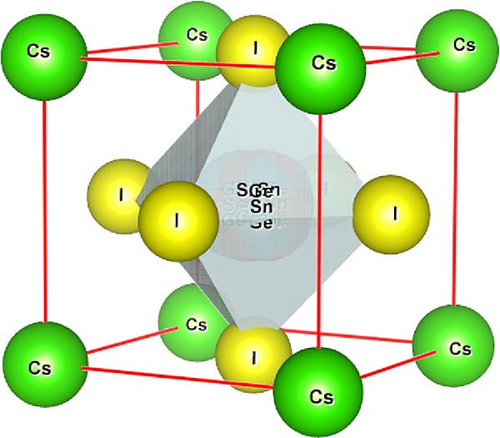
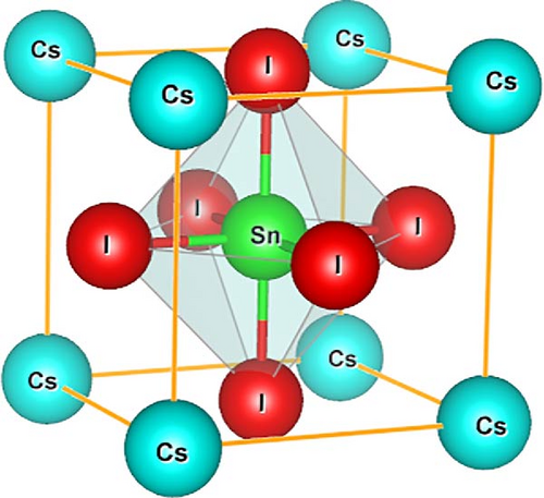
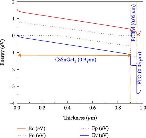
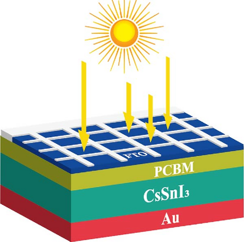
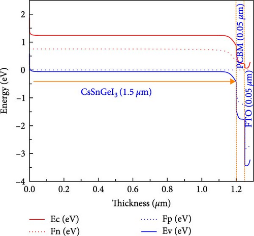
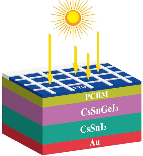
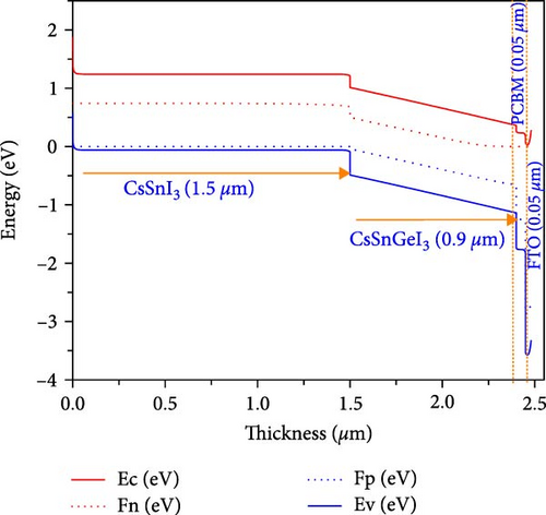
The suggested device architectures include single absorber configurations such as FTO/PCBM/CsSnGeI₃/Au and FTO/PCBM/CsSnI3/Au, along with a DPAL structure, FTO/PCBM/CsSnGeI3/CsSnI3/Au solar cell, along with the crystal structure, cell structure, and associated band diagram, are depicted in Figure 1a–h. The energy band diagrams in Figure 1d,f,h illustrate the conduction band (CB) edge (Ec), valence band (VB) edge (EV), and quasi-fermi levels for electrons (Fn) and holes (Fp) in single and double absorber PSC structures. Figure 1d represents the band alignment of CsSnGeI3-based PSC, where a moderate band bending is observed due to efficient charge transport across the absorber and transport layers. Figure 1f shows CsSnI3-based PSC, which exhibits a slightly lower conduction band edge, leading to a different charge carrier transport behavior. Figure 1h depicts the CsSnGeI3/CsSnI3–based PSC double absorber structure, where the band alignment facilitates improved charge separation and extraction, resulting in potentially enhanced PV performance. The observed band bending variations are attributed to differences in characteristics of materials, including bandgap energy, electron affinity, and defect densities, which affect charge carrier dynamics and recombination rates, ultimately influencing the overall efficiency of the solar cell. The radiative recombination coefficient (B) and Auger recombination coefficient (C) have a significant impact on PSC performance by influencing charge carrier dynamics and recombination losses. A high B accelerates recombination, reducing carrier lifetime, and VOC, while a lower B enhances charge extraction and efficiency. Similarly, Auger recombination dominates at high carrier densities, with a high C causing carrier losses and efficiency drops. The defined properties of every photoactive layer, the interfaces and a comparative study on PV parameters of various absorbers of the suggested PSCs are represented in Tables 1 and 2.

| Parameters | FTO [24, 27] | PCBM [28] | CsSnGeI3 [29–32] | CsSnI3 [33] |
|---|---|---|---|---|
| Thickness (nm) | 50 | 50 | 900 | 1500 |
| Bandgap (eV) | 3.6 | 2 | 1.5 | 1.3 |
| Electron affinity (eV) | 4 | 3.9 | 3.9 | 3.6 |
| Dielectric permittivity (relative) | 9 | 3.9 | 28 | 9.930 |
| CB effective density of states (1/cm3) | 2.2 × 10¹⁸ | 2.5 × 10²¹ | 3.15 × 10¹⁸ | 1 × 10¹⁹ |
| VB effective density of states (1/cm3) | 1.8 × 10¹⁹ | 2.5 × 10²¹ | 3.10 × 10¹⁸ | 1 × 10¹⁸ |
| Electron thermal velocity (cm/s) | 1 × 10⁷ | 1 × 10⁷ | 1 × 10⁷ | 1 × 10⁷ |
| Hole thermal velocity (cm/s) | 1 × 10⁷ | 1 × 10⁷ | 1 × 10⁷ | 1 × 10⁷ |
| Electron mobility (cm2/V s) | 20 | 0.2 | 9.74 × 10² | 1.5 × 10³ |
| Hole mobility (cm2/V s) | 10 | 0.2 | 2.13 × 10² | 5.850 × 10² |
| Donor density, ND (1/cm3) | 1 × 10¹⁸ | 2.930 × 10¹⁷ | 0 | 0 |
| Acceptor density, NA (1/cm3) | 0 | 0 | 1 × 10¹⁴ | 1 × 10¹⁷ |
| Defect type | Acceptor | Acceptor | Neutral | Neutral |
| Bulk defect density, Nt (cm−3) | 1014 | 1014 | 1012 | 1013 |
| Electrons capture cross section (cm2) | 10−15 | 10−15 | 10−15 | 10−15 |
| Hole capture cross section (cm2) | 10−15 | 10−15 | 10−15 | 10−15 |
| Radiative recombination coefficient, B (cm3/s) | — | — | 1 × 10⁻⁹ | 1 × 10⁻¹⁰ |
| Auger recombination coefficient, C (cm6/s) | — | — | 1 × 10⁻²⁸ | 1 × 10⁻²⁹ |
| Parameters | CsSnI3/CsSnGeI3 | CsSnGeI3/PCBM |
|---|---|---|
| Defect type | Neutral | Neutral |
| Electron capture cross-section, σe (cm2) | 10−19 | 10−19 |
| Hole capture cross-section, σh (cm2) | 10−19 | 10−19 |
| Defect position above the highest EV (eV) | 0.6 | 0.6 |
| Interface defect density (cm−2) | 1010 | 1010 |
3. Results and Discussion
3.1. Impact of Active Layer Thickness on Single- and Double-Layer PSCs
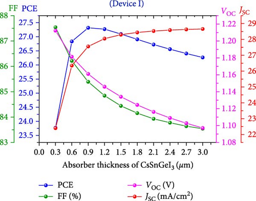
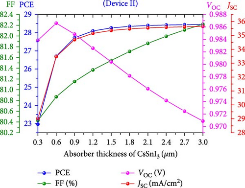
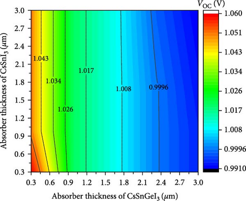
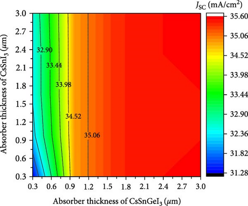
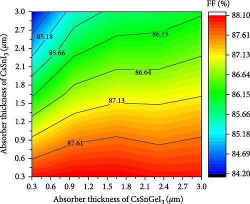
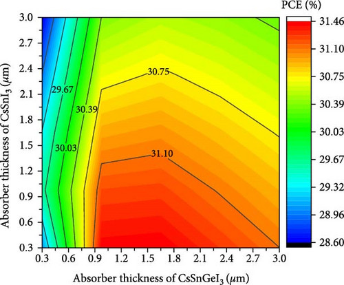
Figure 2a illustrates key performance metrics of a single solar cell (Device I) as a function of absorber layer thickness, showcasing the fill factor (FF), PCE, open-circuit voltage (VOC), and short-circuit current density (JSC). At a thickness of around 200 nm of CsSnGeI3, noticeable changes occur. The VOC is continuously reducing from 1.21 V to almost 1.1 V and FF from approximately 87.5%–83.5% with rising the thickness of CsSnGeI3 active layer owing to the increased recombination losses and resistance issues in thicker layers, which hinder charge transport and collection efficiency. On the other hand, JSC initially increases sharply, then slowly it reaches at almost 28.5 mA/cm2, which is the highest thickness of the active layer. The PCE initially increases, peaking at around 27.5% before declining. These increases are due to enhanced light absorption and better charge separation with thicker layers, before eventually leveling off or slightly decreasing due to the same recombination effects and higher series resistance [35]. This optimal thickness of 900 nm maximizes light absorption and charge transport, aligning with findings from recent studies [36, 37]. As depicted in Figure 2b, the thickness of the active layer impacts several performance indicators. Increasing the absorber layer’s thickness resulted in proportional enhancements in all output parameters of the PSC, except for VOC. The VOC in the graph rises gradually, peaking at around 0.985 V, and then declines continuously. This increase occurs as the absorber layer thickness reaches its optimal point of about 600 nm, enhancing charge separation and collection efficiency. Beyond this optimal thickness, VOC declines because further increases in thickness may cause recombination, resulting in lowering the VOC [38, 39]. In Figure 2c–f, contour plots depict the relation between absorber thickness and solar cell performance, with other variables kept fixed. As shown in Figure 2c, the plot represents that the highest VOC of 1.06 V occurs when both absorber layers are at their thinnest, decreasing progressively to 0.9996 V with increasing thickness. The observed trend underlines the significance of tuning the absorber layer thickness for improved solar cell performance. Proper thickness contributes to a higher VOC by minimizing recombination losses and facilitating better charge separation [40, 41]. In the instance of a bottom absorber, the JSC declines around 32.90 mA/cm2 (Figure 2d), but it grows with the top absorber and the highest JSC of 35.31 mA/cm2. It indicates that greater thickness contributes to improved light absorption and charge creation, consequently boosting the JSC [42, 43]. Figure 2e shows that the FF is became highest at 87.13% at the lesser thickness of both active layers. In Figure 2f, the PCE achieves its maximum of 31.31% when both absorber layers are set to their optimal thickness. Reduced efficiency metrics like 30.03% and 29.67% in the thinner sections of CsSnGeI3 and thicker sections of the CsSnI3, respectively, reveal that going beyond the optimal thickness leads to a decline in PCE.
3.2. Influence of the Active Layer Defect Density
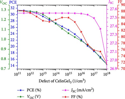
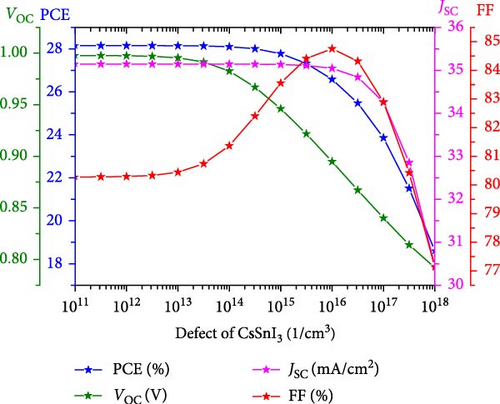
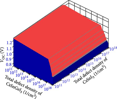
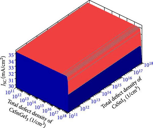
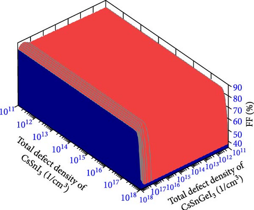
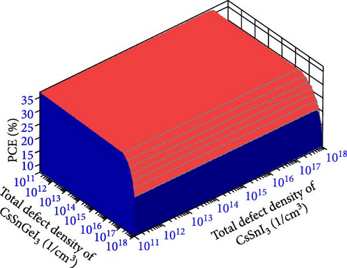
Trap states produced by imperfections in the active layer hinder solar cell performance by capturing charge carriers. Figure 3 illustrates how the density of these defects in the active layer affects overall solar cell performance. The PV outputs in both proposed single-absorber PSCs, as illustrated in Figure 3a,b, decline with rising defect density in the active layer [44, 45]. In case of Figure 3b, FF gradually increases up to 1014 cm−3 and then started decrease. The JSC remains comparatively stable in both scenarios up to a defect density of 1016 cm−3 is achieved, after which it begins to decrease [46]. The influence of defect density in the CsSnGeI3 and CsSnI3 active layers is shown in Figure 3c–f. As the defect density in the absorber layer upsurges, PV outputs decrease, with a marginal decrease rate observed in the upper active layer in comparison to the bottom layer. The VOC, JSC, and PCE achieves a high value of approximately 1.24 V, 35.53 mA/cm2, and 36.68% in Figure 3c–f, respectively, when both absorber layers have low defect densities of 1011 cm−3. The FF decreases from 87.7% to 38.3% in Figure 3e as the defect density upsurges from 1011 cm−3 to 1018 cm−3. The mutual defect density study also offers a practical comprehension of the PSC, which is necessary to create an efficient device that incorporates the DPAL.
3.3. Influence of Acceptor Density of the Active Layer
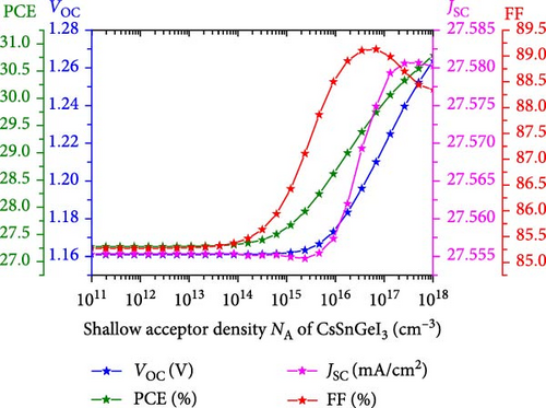
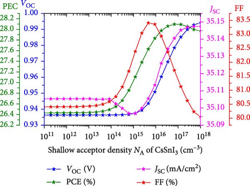
Figure 4a,b illustrates the investigation into the influence of acceptor density variations in CsSnGeI3 and CsSnI3 on cell performance. Figure 4a illustrates that the PV values stay relatively stable until 1014 cm−3. Consequently, an optimal value of 1014 cm−3 [47] was selected, at which point the built-in potential across the device increases, resulting in the isolation of photo-excited charge carriers and the enhancement of various PV parameters, except JSC [48]. Therefore, the acceptor density within the absorber layers is adjusted from 1011 to 1018 cm−3. Moreover, the acceptor concentration of CsSnGeI3 upsurges, which impedes the migration of holes within the absorber cell. Consequently, the enhancing recombination losses and increased series resistance leads the FF to decreased [49]. FF starts to decrease from 88.75% at 1017 cm−3. Optimizing the efficiency of PSCs requires controlling defect density. Modest changes in defect density can improve PCE, VOC, JSC, and FF, but these gains are only temporary, and high defect density can have a detrimental impact on output. In Figure 3b PCE and FF increase, as the acceptor density surpasses 1013 cm−3 in the case of CsSnI3. The PCE increases observably as the acceptor density increases for CsSnI3, with values rising from 26.45% to 28.05%. Where in case of JSC and VOC start to increase from 1015 cm−3, 35.095 to 35.149 mA/cm2 and 0.935 to 0.99 V, respectively. Upon the increment of acceptor density, there is an observable increase in the PCE, with the values elevating from 27.25% to 30.75% and 26.45% to 28.05% for CsSnGeI3 and CsSnI3 absorber-based PSC, respectively.
3.4. Influence of Interface Defect Density (IDD)
Figure 5a–c demonstrates that as the defect density at the interface increases, the performance of PV cells declines particularly for PSCs. This result arises because defects serve as recombination sites for charge carriers, which diminishes essential PV parameters [50]. PSC device efficiency is greatly influenced by deep energy traps that lie closer to the center of the energy bandgap. This leads to a situation where confined charge carriers cannot easily return to the CB or VB and are usually dissipated via nonradiative recombination mechanisms [51, 52]. In the case of a SPAL solar cell, as demonstrated in Figure 5a by (CsSnGeI3/PCBM), all PV outputs remain consistent until a critical IDD of 1011 cm−2 is approached. This is the point at which VOC declines from 1.43 to 0.80 V. Figure 5a also demonstrates that JSC had no major impact by the fluctuation in IDD at CsSnGeI3/PCBM. After rising to 1014 cm−3 at first, FF fell with increasing IDD [39, 53]. The PCE decreased overall from 27.5% to 16.2% because of the collective impacts of VOC, FF, and JSC. Similar patterns were observed when IDD increased from 1010 to 1017 cm−3 in Figure 5b CsSnI3/PCBM (CsSnI3-based SC) and in Figure 5c CsSnI3/CsSnGeI3 (double-layer).
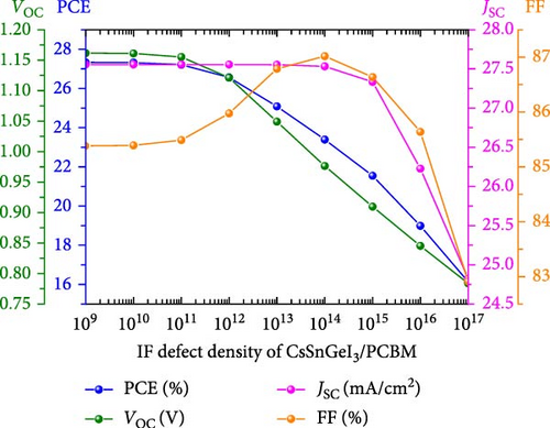
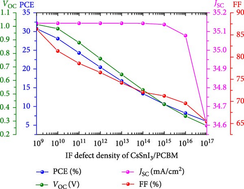
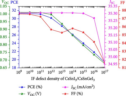
Interface defects serve as recombination sites where photo-generated charge carriers can recombine before arriving at the electrodes. While the current density (JSC) is largely unaffected due to adequate light absorption and charge generation, increased recombination at the defective interface mainly impacts the voltage. As more charge carriers recombine before reaching the external circuit, the effective carrier density decreases, resulting in a drop of the VOC. This voltage lessening happens because VOC is directly linked to the separation between the quasi-fermi levels of electrons and holes. The increased recombination caused by defects reduces this separation, resulting in a lower VOC. Since current generation is primarily determined by the absorbed light and less influence by defect density, the current remains nearly unchanged despite the rise in interface defects [54].
3.5. The Effect of Temperature on the Suggested PSC’s Performance
The functionality of PSCs is greatly impacted by changes in operational temperature [55, 56]. Figure 6 demonstrates the temperature-dependent behavior of critical parameters in single and double-active layer solar cells across a range of 260–440 K. With rising temperatures, the bandgap of the semiconductor narrows [57], enhancing the ability of photons to produce charge carriers. This leads to a rise in JSC for both SPAL and DPAL PSCs [49, 58].

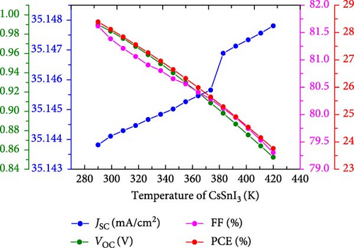
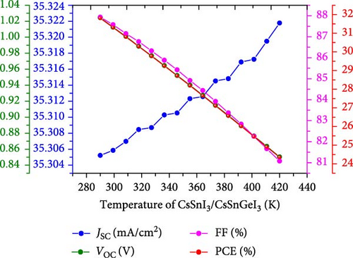
However, VOC, FF, and PCE experience a significant decline with rising temperature. This reduction is largely ascribed to the fact that VOC is directly linked to the bandgap, which becomes narrower at higher temperatures, leading to a drop in VOC. In addition, rising temperatures generally lead to higher JSC, which in turn lowers VOC and ultimately reduces PCE, as demonstrated in Figure 6a of CsSnGeI3-based PSC. A similar trend was observed in Figure 6b of CsSnI3 and Figure 6c of CsSnI3/CsSnGeI3–based PSC when temperature increase from 260 to 440 K.
3.6. J–V Curve and QE Spectra of the Proposed PSC
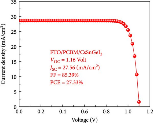
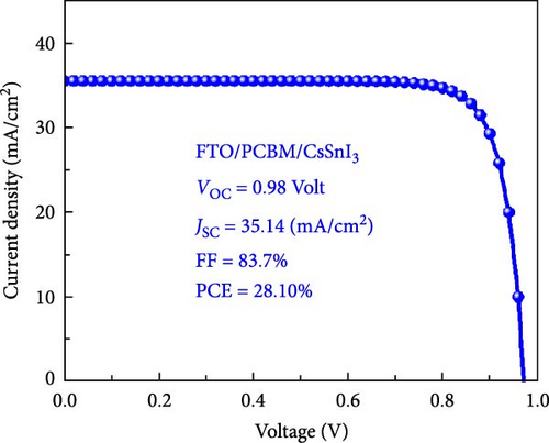
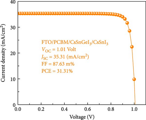
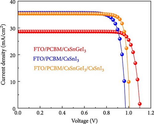
Figure 7a–h has shown the current density–voltage (J–V) properties and quantum efficiency (QE) spectra of PSCs with SPAL and DPAL. The JSC in CsSnGeI3 (single)-based PSC structure in Figure 7a is lower than that of the other two structures (at 27.56 [mA/cm2]), while the CsSnI3 (single)-based PSC has the lowest VOC (0.98 V). The appropriate value of VOC and JSC must be present in order to achieve the maximum PCE. The PSC based on CsSnGeI3/CsSnI3 (double) has a higher JSC of 35.31 mA/cm2 with VOC of 1.01 V exhibiting the maximum PCE of 31.31%.
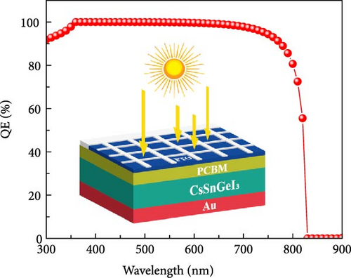
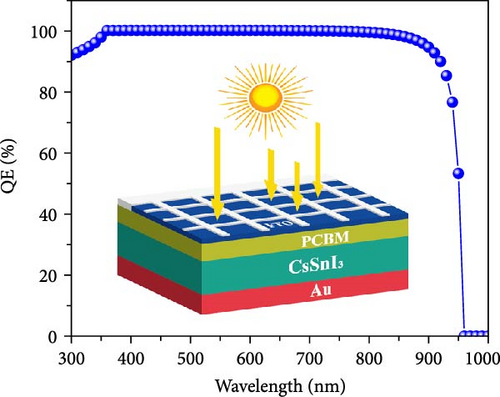
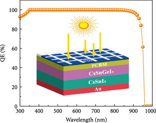
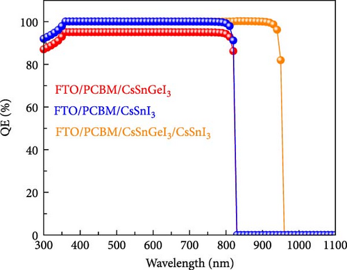
In Figure 7b, the CsSnGeI3 (single)-based PSC due to higher bandgap at 1.5 eV exhibits a significant decrease in QE at 830 nm [59, 60]. Conversely, the CsSnI3 (single)-based PSC in shows a wider QE spectrum extending to 950 nm because of its lower bandgap at 1.3 eV. A similar cutoff point of 950 nm is reached by the double-active layer cell. The QE values is enhanced as for the DPAL of CsGeI3/CsSnGeI3–based PSC in comparison to SPAL PSCs, as the DPAL structure offers a broader absorption spectrum [61]. This structure facilitates the absorption of a wider span of wavelengths associated with photons, effectively covering both narrow and wide energy bandgaps. This broad absorption capability enables the DPALs to capture more solar energy, thereby, enhancing the overall photon conversion efficiency. Additionally, this wider spectral response contributes to improved charge carrier generation across the spectrum, ultimately leading to superior PV performance.
The combination of two distinct perovskite materials, like CsSnGeI3 and CsSnI3, results in a broader absorption spectrum due to their unique bandgaps, allowing for the capture of a broader spectrum of solar wavelengths. This enhances light absorption and increases generation of charge carriers across the spectrum. The complementary absorption properties optimize light harvesting, improving the device’s efficiency in converting solar energy to electricity. Furthermore, the double absorber structure improves the separation and movement of charge carriers, thereby, minimizing recombination losses, which leads to better carrier collection at the electrodes. The configuration also lengthens the optical path within the active layer, allowing for prolonged photon interaction with the material, thereby, increasing the likelihood of absorption and improving the QE curve [62].
Table 3 provides a comparison of the findings of this investigation and those from previous studies. Earlier research on double-absorber solar cells has reported maximum PCE of 27.67%. However, the analysis in this study reveals that the proposed design achieves a significantly higher PCE of 31.31%, outperforming other recent investigations. These results offer valuable insights for the advancement of dual-absorber solar cells, highlighting improved stability and efficiency as key areas of focus for future development.
| Research type | Device structure | VOC (V) | JSC (mA/cm2) | FF (%) | PCE (%) | Reference |
|---|---|---|---|---|---|---|
| Experimental | MAPbBr3/CsPbBr3 | — | — | — | 6.53 | [63] |
| PbS/CdS | 0.30 | 36.30 | 51.40 | 5.59 | [64] | |
| Simulation | FAPbIyBr3-y/CsPbIxBr3-x | 1.11 | 21.00 | 75.00 | 17.48 | [65] |
| CZTS/CZTSe | 0.90 | 25.83 | 69.87 | 17.81 | [66] | |
| La2NiMnO6/Cu2O | 0.79 | 27.89 | 85.52 | 18.89 | [67] | |
| CZTS/Si | 0.84 | 26.94 | 88.30 | 19.40 | [61] | |
| CsPbIBr2/CsPbI2Br | 1.55 | 15.94 | 83.24 | 20.62 | [39] | |
| CsSnI3/CIGS | 1.03 | 32.26 | 80.22 | 26.55 | [68] | |
| FeSi2/CdTe | 0.66 | 49.78 | 83.68 | 27.35 | [69] | |
| MAGeI3/MAPbI3 | 1.41 | 21.706 | 90.32 | 27.67 | [46] | |
| CsSnGeI3/PCBM/FTO | 1.16 | 27.56 | 85.39 | 27.33 | This works | |
| CsSnI3/PCBM/FTO | 0.98 | 35.14 | 81.37 | 28.10 | — | |
| CsSnI3/CsSnGeI3/PCBM/FTO | 1.01 | 35.31 | 87.63 | 31.31 | — | |
4. Conclusions
This study has shown the immense potential of using a double absorber layer design in PSCs with CsSnGeI3 and CsSnI3 perovskites. Through detailed simulation and optimization, the design achieved an impressive PCE of 31.31%, along with a JSC of 35.31 mA/cm2, a VOC of 1.01 V, and an FF of 87.63%. These results outperform those of traditional single absorber PSCs, highlighting the effectiveness of the dual absorber approach in improving light absorption and charge carrier dynamics. The study underscores the importance of optimizing parameters such as absorber layer thickness, defect density, and doping concentrations to attain high efficiency in PSCs. Additionally, the use of lead-free materials like CsSnGeI3 and CsSnI3 not only addresses environmental concerns but also enhances the structural and chemical stability of the devices, making them more suitable for large-scale production. The research also offers valuable insights into the thermal stability and defect tolerance of the proposed PSC configurations, paving the way for future innovations in the field. With its broad absorption spectrum and improved charge transport properties, the dual absorber structure marks a significant advancement in PV technology. Despite the remarkable efficiency gains achieved with double-absorber PSCs, defect-induced recombination, scalability, and environmental concerns remain significant obstacles to commercialization. Subsequent research efforts should concentrate on increasing the durability of materials, optimizing fabrication methods, and integrating tandem architectures to further improve efficiency and long-term viability.
Conflicts of Interest
The authors declare no conflicts of interest.
Funding
This work is supported by the Deanship of Research and Graduate Studies at King Khalid University for funding this work through the Large Groups Research Project under Grant number RGP2/71/46.
Acknowledgments
Ahmad Irfan extends his appreciation to the Deanship of Research and Graduate Studies at King Khalid University for funding this work through the Large Groups Research Project under Grant number RGP2/71/46.
Open Research
Data Availability Statement
The data are available from the corresponding author upon reasonable request.


