Triple-Rectangular Band Rejection Monopole Ultrawide-Band Antenna with Spiral Electromagnetic Band-Gap Structures
Abstract
A printed ultrawideband (UWB) monopole antenna with triple-rectangular band rejection characteristics at WiMAX, WLAN, and satellite band is presented in this paper. The frequency selectivity of each rejection band is improved by employing the mutual coupling of two spiral-shaped electromagnetic band-gap (EBG) structures. The proposed design consists of the modified rectangular patch with a compact size of 23.5 × 23 mm2 having a partial ground plane and three pairs of spiral EBGs. To mitigate the interference from the WiMAX band, one pair of the spiral is coupled with the microstrip line, which exhibits band rejection of 3.3–3.7 GHz (11.42%). WLAN band from 5.1 to 5.9 GHz (14.5%) is notched by another pair of spiral EBGs designed on the opposite side of the radiating patch, and for satellite band rejection, two spiral EBGs are embedded on the opposite side of the microstrip line which ranges from 7.25 to 7.8 GHz (7.3%). Moreover, peak gain, radiation pattern, and time domain behavior of the proposed design are also investigated in Ansys Electronics Desktop 17.0 to find its suitability in UWB applications.
1. Introduction
The exponential growth of wireless applications over time demands an increase in operating bandwidth. Ultrawideband systems provide the solution for such applications by offering wide impedance bandwidth after the Federal Communication Commission (FCC) granted permission for the use of 3.1–10.6 GHz frequency spectrum without the need for a license [1]. UWB systems have inherent merits such as low power spectral density, very high data rate, less probability of interception, and rejection of multipath effect. UWB planar antennas are an important part of UWB systems because of their low profile, compact size, easy fabrication, and ease of integration with printed circuit boards. However, due to extreme bandwidth, an inevitable overlap exists between UWB band systems and several narrow bands systems such as worldwide interoperability for microwave access (WiMAX; 3.3–3.6 GHz), wireless local area network (WLAN; 5.15–5.85 GHz), satellite band (7.25–7.75 GHz), and ITU band (8.0–8.565 GHz).
To avoid interference from such systems, the use of a UWB antenna with notch characteristics is required in the UWB system. Numerous approaches have been applied for the notched band antenna design in literature such as coupling of parasitic elements to radiating patch [2–4], by etching slots in patch [5–7], using split rings [8–11], and step impedance resonator [12]. Configurable UWB designs can be implemented with varactor diodes [13], and switchable notch bands can implemented using PIN diode or MEMS [14, 15].
Several electromagnetic band-gap (EBG) structures have been introduced in recent years to provide isolation in MIMO designs [16–18] and to create a notch in UWB antennas [19–22]. In [19], to create a notch band at the WLAN band, four conventional mushroom-type EBG structures with dimensions 8.5 × 8.5 mm2 have been used. In [20], conventional mushroom-type EBG structures with an edge length of 5.7 mm and edge-located vias mushroom-type EBGs with an edge length of 4.9 mm are compared to create a notch for the WiMAX band. However, the mentioned EBGs occupy large space, and compact antennas with notch characteristics are the demand for printed circuits. To reduce the size of EBGs, many techniques are explained in the literature. Further inductance-enhanced modified mushroom EBG structures are investigated in [21] to tune the notch from the WLAN band to the WiMAX band with 34% compactness. In [22], four defective ground compact EBG structures present at both sides of the feedline create a notch for WiMAX and WLAN band with a compactness of 46% and 45%, respectively, over mushroom EBG structures.
Moreover, the designs discussed above create speculated notches and do not reject the undesired band efficiently. A few researches are present in the literature on antennas with rectangular notch characteristics. To achieve wideband notch rejection with high selectivity, authors in [23, 24] suggested that at least two notch-creating structures are required to reject a single notch. An elliptical patch antenna is suggested in [23] with two EBGs present on the feeding line to create a rectangular notch with controlled notch bandwidth. In an ACS-fed antenna [24], the coupling of the strip and slit creates a rectangular notch band with controllable bandwidth. However, the designs suggested in the literature have large and complicated structures.
In this work, a compact printed monopole antenna design having six spiral EBGs has been proposed to reject WiMAX, WLAN, and satellite bands efficiently with rectangular notch characteristics. To obtain compactness in antenna design, spiral EBGs have been utilized. The miniature size of spiral EBGs for particularly low frequencies is obtained by etching spiral strips from the metallic patch, which leads to enhanced inductance and ultimate reduction in the size of EBG structure as discussed in Section 3. To realize rectangular notch characteristics, mutual coupling of two EBGs per notch is implemented. EBG1 and EBG2 present on both sides of the feed line reject WiMAX band. EBG3 and EBG4 embedded on the opposite side of the feed line are used to notch the satellite band, while EBG5 and EBG6 are present on opposite sides of the radiating patch for rejection of the WLAN band. By tuning the parameters of spiral EBGs, the resonant frequency and notch bandwidth can be controlled. Ansys Electronic Desktop 17.0 has been used for simulation. It primarily uses the finite element method (FEM) for its electromagnetic simulations. It helps to design the various electronic circuits faster. The simulation from Ansys helps to solve the critical design features.
This paper is divided into four sections. In Section 2, antenna geometry and simulated results for parametric analysis are discussed. In Section 3, an analysis of the proposed antenna is done. Section 4 presents the time domain analysis of the proposed design. Measured results are shown in Section 5. Besides, this proposed design is compared with existing literature. From the simulated and measured results, it can be concluded that the proposed antenna design has several advantages such as compact size, triple-rectangular notch band performance, as well as bandwidth-controlled features.
2. Antenna Design
The proposed antenna designed on RogersRT/Duroid 5880 having εr = 2.2 and loss tangent 0.0009 with a thickness of 1.6 mm is shown in Figures 1(a) and 1(b). The antenna has dimensions of Wsub × Lsub = 23.5 × 23 mm2 fed with 50 Ω impedance microstrip line. The antenna’s basic structure consists of a radiating patch with a partial ground plane with a slot to achieve ultrawide bandwidth as shown. To create triple notches, this antenna contains three pairs of spiral EBG structures. One pair of spiral EBG structures which is creating a notch at the WiMAX band is present on both sides of the feed line, while another pair of spiral EBGs creating notch for the X-band is present on the opposite side of it. And third pair of spiral EBGs, present on the opposite side of the patch, is responsible for creating a notch at the WLAN band. The optimized parameters of the proposed antenna are mentioned in Table 1.
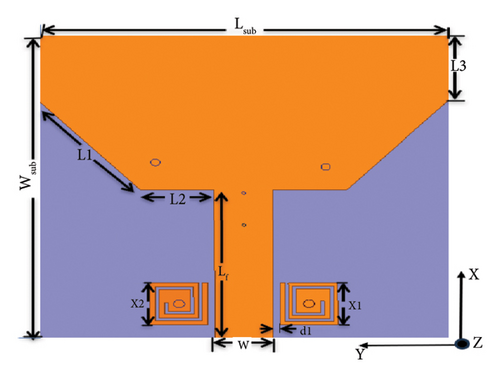
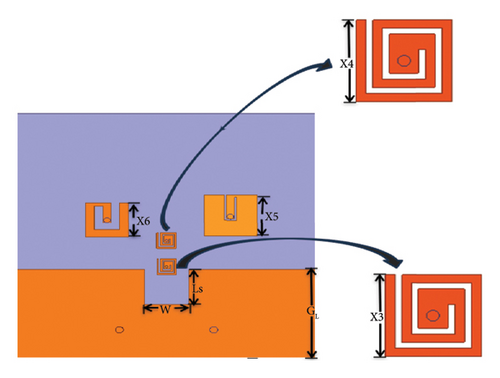
| Parameter | Value (mm) |
|---|---|
| Wsub | 23.5 |
| Lsub | 23 |
| L1 | 9 |
| L2 | 4 |
| L3 | 5 |
| Lf | 11.5 |
| Wf | 3.25 |
| x1 | 3.2 |
| r1 | 0.3 |
| a1 | 0.2 |
| b1 | 0.25 |
| c1 | 1.1 |
| x2 | 3.2 |
| r2 | 0.3 |
| a2 | 0.2 |
| b2 | 0.3 |
| c2 | 0.9 |
| x3 | 3.3 |
| r3 | 0.25 |
| a3 | 0.65 |
| b3 | 0.2 |
| c3 | 2.4 |
| x4 | 4 |
| r4 | 0.25 |
| a4 | 0.15 |
| b4 | 1.55 |
| c4 | 2.2 |
| x5 | 1.5 |
| R5 | 0.1 |
| a5 | 0.13 |
| b5 | 0.15 |
| c5 | 0.67 |
| x6 | 1.5 |
| r6 | 0.1 |
| a6 | 0.11 |
| b6 | 0.15 |
| c6 | 0.55 |
| Lg | 23 |
| Ls | 3.4 |
| Ws | 3.4 |
2.1. Spiral EBG Structure
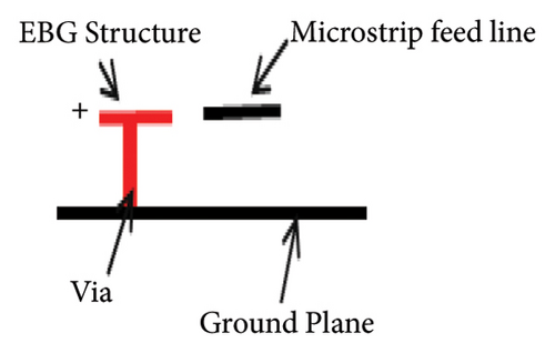
A spiral EBG structure is formed by replacing the patch of mushroom EBG with a spiral-shaped metallic branch with a via at its center. Spiral EBG structures are very compact in comparison to mushroom EBG structures for creating notches at a particular frequency [25]. In the proposed design, six spiral EBGs (i = 1 to 6) have been employed. As shown in Figure 2, each spiral EBG is composed of a rectangular patch having a side xi and j number of line segments. A spiral-shaped metallic branch has number of line segments each having width bi, and the spacing between two length segments is ai. A via with radius ri is located at the center of the patch, length lij represents the jth length of the etched element in ith EBG, the number of turns in the spiral branch is N, and ti is the thickness of the length segment. The operating mechanism of EBG structures can be explained through an equivalent circuit as shown in Figure 3.
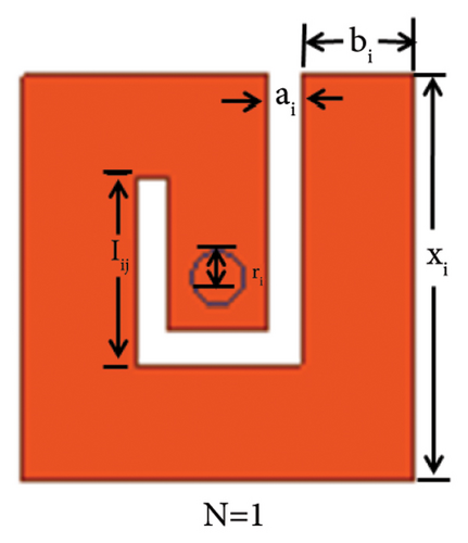
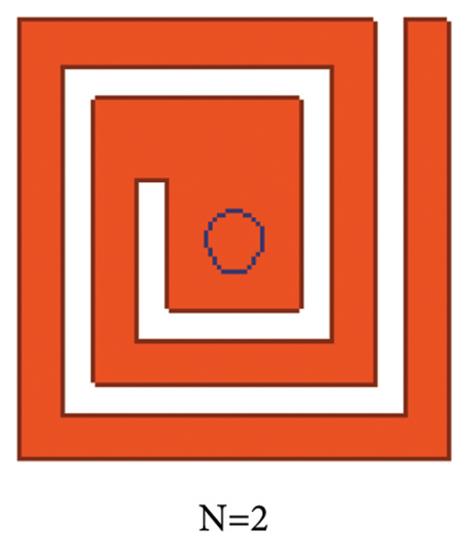
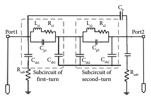
Thus, spiral-shaped EBGs tend to increase the total inductance which leads to a decrease in the size of EBGs for lower-frequency notch operation.
In the proposed design, the rectangular notch is achieved with mutual coupling of two EBGs at each notch frequency.
3. Antenna Analysis
3.1. UWB Antenna Design
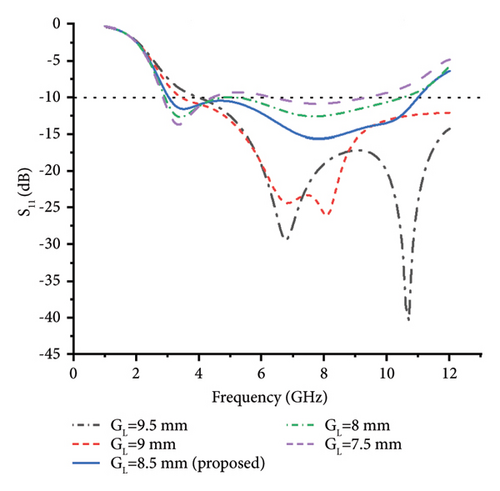
First, the patch antenna covering the UWB band without notches is designed. To study the effects of partial ground plane, the parametric analysis has been performed in Ansys Electronic Desktop 17.0 for different values of ground length GL. It has been observed from Figure 4 that only for GL = 8.5 mm, the UWB range from 3 GHz to 11 GHz has been obtained.
3.2. WiMAX Band (3.3–3.6 GHz) Rejection
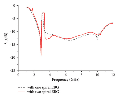
To create a wide notch, two spiral EBGs (i = 1, 2) are loaded on both sides of the microstrip feedline. As mentioned above, the resonant frequency of each EBG depends upon its various dimensions. As shown in Figure 5, with spiral EBG1 structure, the notch is created from 3.3 GHz to 3.7 GHz, which does not cover the whole WiMAX band with equal attenuation. A wide notch is realized by introducing two spiral EBG structures and after optimizing the different dimensions (a1, b1, l11, a2, b2, and l21). By mutual coupling of two EBGs, a wide notch has been created from 3.3 GHz to 3.7 GHz. Here, the parametric study is shown for lengths l11 and l21 in Figures 6(a) and 6(b), respectively. Figure 6(a) shows the effect of length l11 on reflection coefficient. As the value of l11 increases from 0.7 mm to 0.9 mm, the lower notch frequency decreases while the upper frequency is constant. Similarly, in Figure 6(b), as the length l21 value is increased, the lower notch frequency remains the same while the upper one decreases, hence bandwidth also varies. Thus, EBG1 controls the lower notch frequency, and EBG2 is responsible for the upper one.
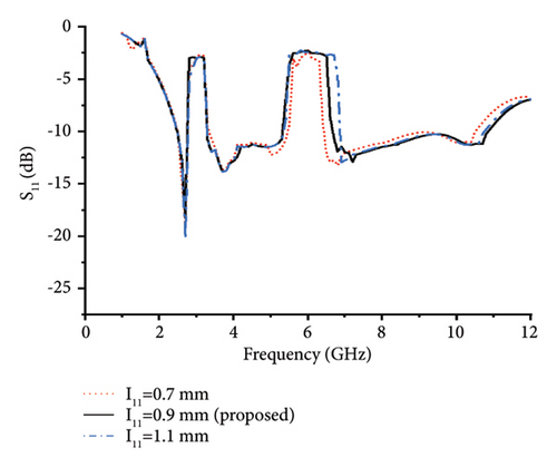
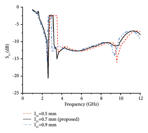
The optimized values for l11 = 0.9 mm and l21 = 0.7 mm are achieved after parametric analysis.
Figure 7 shows the effect of the gap between the length segments on the reflection coefficient. It is clear from Figure 7(a) as the gap a2 increases from 0.05 mm to 0.35 mm, the notch frequency shifts to the left-hand side. Similar variations can be seen in Figure 7(b) when the width of the line segment increases. Thus, to change notch frequency without any effect on bandwidth, variations in a2 and b2 parameters can be done.
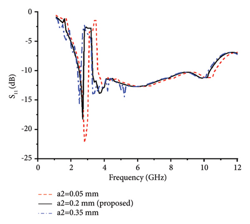
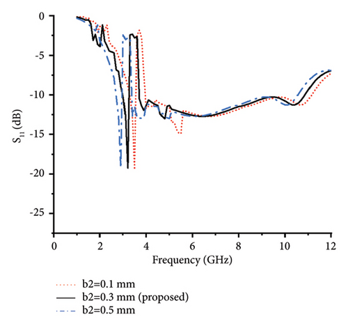
The above observations indicate that by varying the different parameters of EBG 1 and 2, the notch frequency and bandwidth can be controlled.
3.3. WLAN Band (5.15 GHz–5.825 GHz) Rejection
Another pair of spiral EBG structures (i = 5, 6) is embedded on the back side of the patch to achieve a notch at the WLAN band. To achieve a rectangular notch, parameters (a5, b5, l51, a6, b6 and l61) of EBG5 and EBG6 are optimized. As the number of turns increases in spiral EBG, the bandwidth decreases, so the EBGs with single turn N = 1 are designed here, because of the wide bandwidth of the WLAN notch. The S11 characteristics of the proposed design with WiMAX and WLAN bands are shown in Figure 8. To achieve a rectangular WLAN band notch, l51 and l61 parametric analysis have been shown in Figures 8(a) and 8(b).
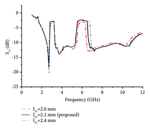
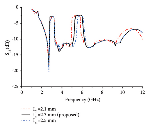
Figure 8(a) shows that l51 length of EBG5 is responsible for controlling the upper notch frequency of the WLAN band. The lower frequency is controlled by variation in l61 length of EBG6 as shown in Figure 8(b). Thus, by mutual coupling of EBG5 and EBG6, the rectangular notch is obtained for the WLAN band.
3.4. Satellite Band Rejection (7.25 GHz–7.75 GHz)
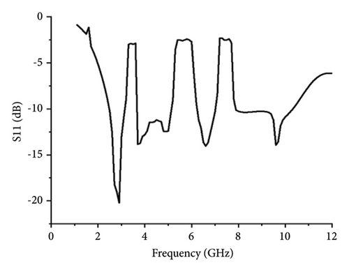
Two spiral EBGs are present along the feed line, and another two are embedded back side of the patch. So, two avoid coupling from already present EBGs, and another two spiral EBGs (i = 3, 4) with N = 2 are introduced on the back side of the feed line to create a notch at the satellite band. First, an irregular notch is created with EBG3 by optimizing parameters such as gap a3, width b3, and length l31.
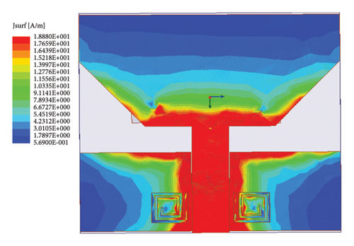
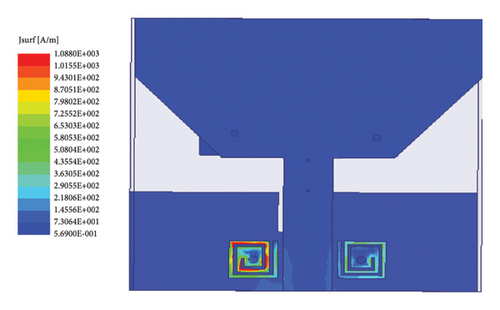
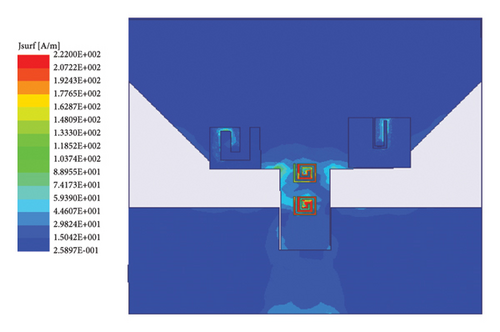
To achieve a wide notch, EBG4’s parameters a4, b4, and l41 are optimized to merge the individual notches. The S11 characteristics of the proposed design with WiMAX, WLAN, and satellite band rejection are shown in Figure 9. Figure 10 shows simulated surface current distribution at different frequencies. It can be observed in Figure 10(a) that the surface current is flowing mainly in the feed line as well as the sides of the radiating patch and negligible current is flowing around the notch structures. At 3.4 GHz, current concentrates at EBG1 and EBG2. EBGs work by absorbing current at a particular frequency, so no radiation occurs as shown in Figure 10(b). Similarly, at 5.5 GHz, current flows more at EBG5 and EBG6 as depicted in Figure 10(b). At 7.6 GHz, current surrounds on EBG3 and EBG4 as shown in Figure 10(c). So, the simulated results for surface current distribution verify that EBG1 and EBG2 are creating a notch at the WiMAX band and a notch at the WLAN band is due to EBG5 and EBG6. At the same time, EBG3 and EBG4 are responsible for notch generation at the satellite band.

4. Analysis in Time Domain
In order to evaluate the time domain analysis of UWB systems, two important parameters are the dispersion analysis and group delay.
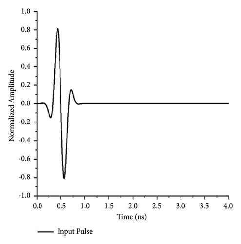
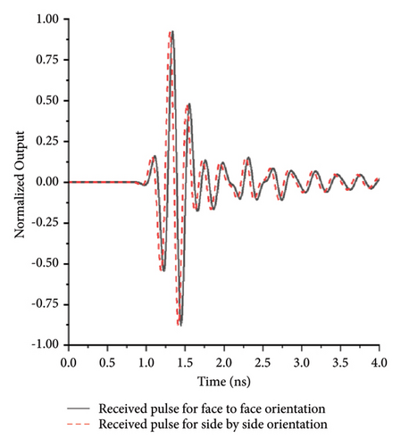
In UWB systems, narrow pulses are used for transmitting the signal, so to check the performance of such systems, time domain analysis is very important. To measure the simulated dispersion in ANSYS Electronics Desktop, two identical antennas are placed at a distance of 200 mm (greater than far field distance) in side-by-side and face-to-face configurations, and excited with a fifth-order Gaussian broadband pulse (according to FCC mask for UWB systems) has been shown in Figure 11(a). The normalized amplitude of received waveforms for side-by-side and face-to-face configurations is almost similar as shown in Figure 11(b), and also, some ringing effect is present in both the waveforms. This effect is mainly due to the presence of spiral EBGs (notch-creating structures).
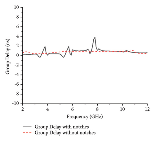
Group delay is measured to find the distortion in the received pulse radiated by the antenna at a particular distance. In Figure 12, simulated group delay for the proposed design with and without notches has been presented. It is clear from Figure 12 that group delay without notches is almost linear over the whole bandwidth and variations lie in the range of 1 ns. On the other side, for an antenna with notches, the group delay exceeds 1 ns near notch frequencies with a maximum value of 4 ns.
5. Analysis of Measured Results
5.1. Measured |S11|
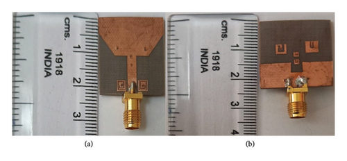
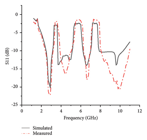
The proposed antenna has been fabricated on Rogers RT5880 with a thickness of 1.6 mm as shown in Figure 13. To validate the simulated results, experimental verification was performed. Figure 14 shows the |S11| characteristic measured by a network analyzer ANRITSU VNA model MS 2038C and compared with simulated results. It can be seen from Table 2 that measured results are in good agreement with simulated results except at higher frequencies. The reason behind this deflection is mainly due to the scarcity of fine etching of spiral-shaped slots.
| Proposed design | Resonant frequencies (GHz) | Operational bandwidth (GHz) |
|---|---|---|
| Simulated | 2.9, 3.8, 6.8, 9.8 | 2.5–3.1, 3.8–5, 6.4–7, 7.9–11 |
| Measured | 2.88, 4.2, 6.85, 10 | 2.5–3.12, 4–5.8, 6.41–7, 8.1–11 |
5.2. Experimental Radiation Pattern and Gain
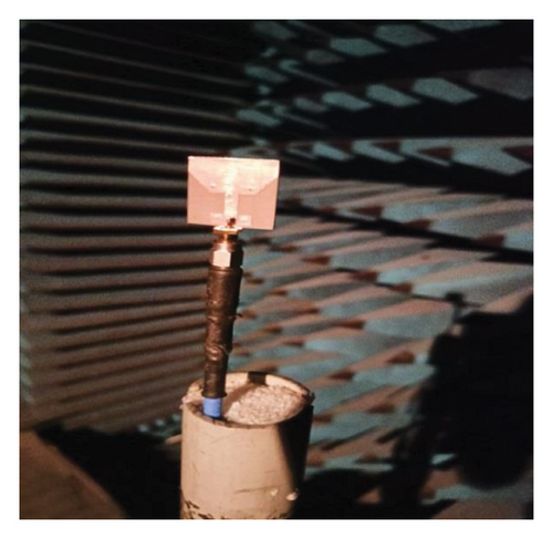
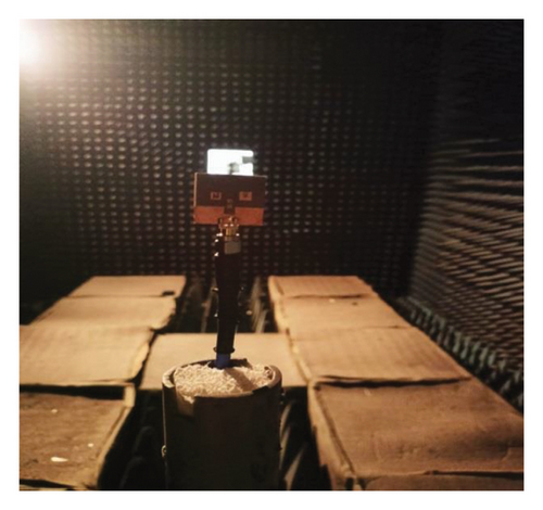
For radiation pattern measurement, the proposed design was placed in a microwave–protected anechoic chamber as shown in Figure 15. Copolarization happens when the electric field of a wave aligns with the E-plane of an antenna, while the magnetic field aligns with the H-plane. Cross-polarization, on the other hand, occurs when the electric and magnetic fields of the wave are not aligned with the antenna’s E-plane and H-plane, respectively. Copolarization and cross-polarization E-plane radiation pattern and H-plane radiation pattern at 3 GHz, 6 GHz, and 9 GHz are drawn in Figure 16. As shown in Figure 16, the level of cross-polarization is very low compared to the copolarization level.
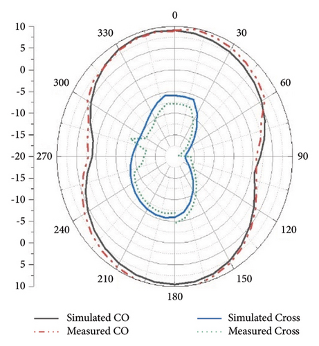
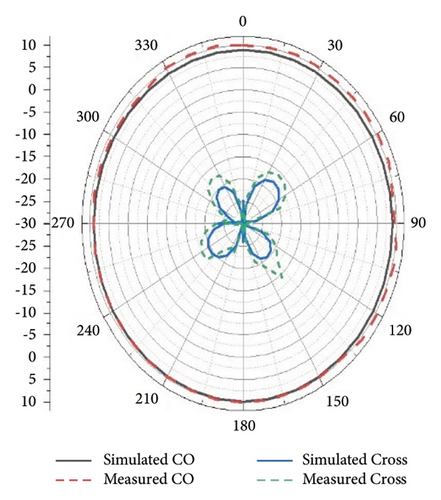
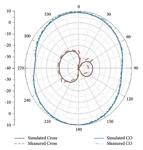
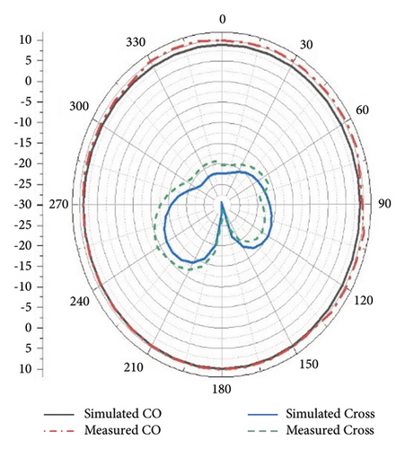
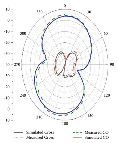
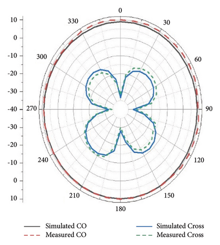
Both the measured and simulated radiation patterns (that are in agreement) for E-plane and H-plane at 3 GHz, 6 GHz, and 9 GHz are presented in Figure 16. For H-plane, nearly omnidirectional radiation pattern has been observed for both measured and simulated results. However, a slight deterioration in the shape is observed at 9 GHz. Doughnut-shaped radiation patterns are observed for E-plane measured and simulated results.
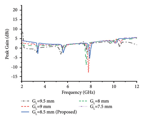
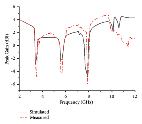
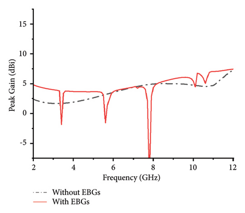
In Figure 17(a), the parametric analysis of peak gain with respect to ground length GL has been shown. For GL = 8.5 mm, the gain is optimum for all the notches. Figure 17(b) shows that the peak gain of the antenna extends upto 5 dBi in the experimental result for passband frequencies. However, in notch bands, the gain decreases to −2.4 dBi for the WiMAX band, −2.2 dBi for the WLAN band, and −6 dBi for the satellite band. Figure 17(c) shows the effect of EBGs on gain performance of the proposed work. The graph depicts that the presence of EBGs enhances the overall gain in operational bandwidth except at notch frequencies.
In the end, the proposed antenna has been compared with recently reported designs in the literature in Table 3. Designs in [27, 28] have comparatively small areas, but the number of notch bands is only one. Common mode and differential mode operation were used in [29] to achieve two notch bands; however, time domain characteristics were not investigated to check the suitability of the antenna for UWB operations. In [30], the antenna was relatively greater in size with only the WLAN band notched. To achieve the first rectangular notch in [31] from 5.94 to 7.5 GHz, resonances of U-slot and SRRs pair are merged. Moreover, the mutual coupling of a pair of EBG structures is utilized to reject 8.02 GHz–10.46 GHz. However, the antenna is comparatively large. In [10], three rectangular notches have been created with the mutual coupling of two pairs of EBGs and one pair of SRR. However, the design has not been analyzed in time domain to check the suitability in UWB applications.
| Reference | Antenna size (mm3) | Technique used | Number of rectangular notches | Frequency range of notched band (GHz) | Time domain analysis |
|---|---|---|---|---|---|
| [27] | 8.5 × 22 × 0.8 | Open-ended slot and a short-ended split-ring | 1 | 5.15–5.85 | No |
| [28] | 28 × 18 × 0.8 | Common mode and differential mode operation | 2 | 5.1–6, 7.83–8.47 | No |
| [29] | 16 × 25 × 1.52 | EBGs | 1 | 5-6 | No |
| [30] | 25 × 25 × 1.6 | EBG and U-slot | 1 | 5–5.91 | Yes |
| [31] | 25 × 25 × 1.6 | U-slot, SRRs pair, and dual EBG structures | 2 | 5.94–7.5 and 8.02–10.46 | Yes |
| [10] | 20 × 26 × 1.52 | EBGs and SRRs | 3 | 3.4–3.9, 5.15–5.82 and 7.25–7.75 | No |
| Proposed design | 23.5 × 23 × 1.6 | Spiral EBGs | 3 | 3.3–3.7, 5.1−5.9, 7.25−7.8 | Yes |
In Table 4, the comparison has been done on the basis of another important parameters, i.e., cross-polarization and gain with similar existing literature based on UWB with notched bands. The excellence of the proposed structure lies in the fact that compact structures (spiral EBGs) have been utilized to achieve three rectangular bands, which are responsible for an overall reduction of antenna size. Also, the level of cross-polarization for the proposed structure is very low as compared to other compared structures with moderate gain.
| Ref. No | Antenna size (mm3) | Technique used | Number of notches | Peak gain (within UWB) | Cross-polarization level |
|---|---|---|---|---|---|
| [32] | 28 × 30 × 0.762 | Pi-shaped slots and EBGs | 4 | 4.5 | High |
| [33] | 30 × 36 × 0.762 | Spiral EBGs | 3 | 4.7 | — |
| [34] | 32 × 39 × 0.762 | CSRR | 1 | 4.7 | — |
| [35] | 38 × 39 × 0.79 | Concentric rectangular loops and split rings | 3 | 8.0 | Medium |
| Proposed design | 23.5 × 23 × 1.6 | Spiral EBGs | 3 | 5.0 | Low |
6. Conclusion
With a high compact size of 23.5 × 23 mm2, a triple-rectangular notched band UWB antenna was fabricated and analyzed. The compact spiral EBG structure pairs that were used to create three notch bands of 3.5 GHz, 5.5 GHz, and 7.5 GHz were observed in the operating bandwidth of 3–11 GHz. The highest peak gain observed is 5 dBi, but it diminishes abruptly up to −6 dBi at notch bands. Also, a good agreement is achieved between the measured and simulated results of the proposed design. Moreover, the advantages of compact size and rectangular notch characteristics make the proposed design a good choice for practical UWB applications.
Conflicts of Interest
The authors declare that they have no conflicts of interest.
Open Research
Data Availability
The data that support the findings of this study are available from the corresponding author upon reasonable request.


