Perovskite Solar Cells With Modified Carbon Electrode and CuSCN Interlayer Processed Under Ambient Conditions
Abstract
Carbon-based perovskite solar cells (PSCs) have the advantages of a long lifetime and are compatible with highly scalable manufacturing processes. The use of carbon electrodes and the absence of a hole selective layer (HSL) promote a simplified fabrication process. However, the efficiency of HSL-free carbon-based PSCs is inferior to PSCs that utilize metal electrodes and HSL due to poor hole extraction at the perovskite/carbon interface. To overcome those issues, researchers added an interlayer on the perovskite/carbon interface or incorporated additive material into the carbon layer. However, there is limited research on utilizing both strategies to improve carbon-based PSC performance. Here, we use CuSCN as an interlayer between the perovskite/carbon interface and a carbon additive in carbon-based PSCs. By utilizing both strategies, the charge transfer of carbon-based PSC was significantly improved compared to carbon-based PSC utilizing only one improvement strategy. Confirmed by photoluminescence (PL) and electrochemical impedance spectroscopy (EIS) characterizations, the CuSCN interlayer and CuSCN-incorporated carbon electrode enable more efficient hole transfer, resulting in an increased power conversion efficiency from 0.58% to 5.06%. The proposed PSC structure shows promising results for further improving carbon-based PSC performance.
1. Introduction
The development of solar cells began in the 1960s. At present, solar cell modules are commercially available and have become the leader in renewable energy sources. It is expected to take the largest portion in renewable electricity generation for the Net Zero program [1]. Currently, silicon-based solar cells have been the benchmark in solar cell technology for their lifetime, and the manufacturing process is mature enough for mass production. Extensive research has been done in multicrystalline silicon solar cells, with a maximum efficiency reaching 23.3%, while commercially available solar cells have a typical efficiency of around 14%–19% [2]. To commercialize the state-of-the-art research cell, the manufacturing cost will be high due to the complexity of the structure, thus potentially raising its price in the market. Therefore, solar cell development has shifted to searching for high-performance and low-cost active materials with a simple manufacturing process, pushing the boundary of the first-generation solar cell.
In 2009, Kojima et al. introduced the potential of perovskite as an active material for solar cells [3]. Perovskite has been a well-known material for several years. Its name is derived from Russian mineralogist Lev A. Perovski. At first, Miyasaka et al. adopted perovskite in a dye-sensitized solar cell (DSSC) structure and yielded an efficiency of 3.8%. Then, a solid-state type was developed to avoid the corrosive electrolyte in perovskite DSSC and successfully improved its efficiency and stability [4]. This type of solar cell has become known as a perovskite solar cell (PSC) and has been extensively investigated because of the ease of fabrication method and low cost. Nowadays, the leading PSC performance has surpassed the multicrystalline silicon solar cell and has the potential to become the next-generation solar cell.
Most PSCs use an organic hole selective layer (HSL) such as Spiro-OMeTAD or PTAA and noble metal electrodes (e.g., gold or silver). These materials become a limitation in the effort to commercialize PSC. Organic HSLs are known for decreasing PSC stability. Also, organic HSL and noble metals are notoriously expensive. Further, metal electrodes, such as gold, can diffuse through the HSL, permanently degrading the PSC [5]. Negative impacts also happen for silver where the degradation of perovskite material reacts with silver, forming a silver iodide layer that has lower conductivity [6]. Considering these issues, an investigation into alternative HSL and electrode material for PSC becomes an intriguing research topic.
Common metals such as aluminum and copper can be used for counter electrodes. However, the deposition technique requires vacuum processing, such as thermal evaporation or sputtering, which is energy-intensive. An alternative material is carbon. Its work function is comparable to gold and chemically stable. A vast selection of deposition techniques, including low-cost ones (e.g., screen printing, doctor blade, or clamping), add more potential for carbon to be used as counter electrodes [7–9]. The first use of carbon as a PSC counter electrode was introduced by Ku et al. [10]. Using a mesoscopic structure, the perovskite solution was dropped onto the carbon layer and then seeped into the mesoporous ZrO2 and TiO2 layer. The reported PSC produced a power conversion efficiency of 6.64%. Further study found that the hydrophobicity of carbon helps the stability of the PSC [8]. CH3NH3PbI3 (methylammonium lead iodide, MAPbI3) perovskite is commonly used in the development of PSC. It is known to be susceptible to water and can degrade by exposure to moisture in the environment. Furthermore, carbon has the ability to selectively transfer the photogenerated hole from the perovskite layer. This absence of HSL simplified the PSC structure (HSL-free PSC).
The merit of carbon-based PSCs led to the development of large-area PSCs. Hashmi et al. demonstrated air-processed carbon-based PSC using inkjet printing, which is a highly scalable deposition method and achieved an efficiency of 6.7% for an active area of 0.16 cm2 [11]. However, the development of large-area PSC has an issue regarding the coffee ring effect, which rises due to different evaporation rates of solvent during the deposition process. One attempt is to develop a green perovskite precursor. The precursor was then applied to carbon-based PSC using inkjet printing and achieved an efficiency of 10.07% for an active area of 52.4 cm2 [12]. On the other hand, the slot die coating technique was also successfully employed to fabricate carbon-based PSC [13].
Despite the many advantages, the performance of carbon-based PSCs is still lower than PSCs with metal counter electrodes. There is a significant difference in energy level alignment in the perovskite/carbon interface, resulting in the limited charge transfer. This results in a low value of open-circuit voltage (VOC) [14]. One attempt to overcome that problem is by incorporating an additive to the carbon counter electrode or adding an interlayer in the perovskite/carbon interface. Several HSL materials such as CuS, PANi, or WO3 have previously been utilized as carbon additives and improved the performance of carbon-based PSCs [15–17]. Wu et al. added CuSCN as an HSL between a carbon nanotube electrode and the perovskite layer, increasing efficiency from 12.25% to 15.13% [14]. Similar results were reported by Yang et al., where CuSCN was deposited on top of a carbon counter electrode, resulting in improved efficiency compared to HSL-free PSCs [18]. Other research groups also utilized and optimized CuSCN in carbon-based PSCs and studied its influence on performance [19–22]. From the mentioned literature, there are two strategies to improve the performance of carbon-based PSCs. First is the use of hole-selective material (HSM) as an interlayer on the perovskite/carbon interface, and second is modifying the carbon electrode by incorporating an additive. The presence of an HSM as an interlayer in a carbon-based PSC facilitates better charge transfer and compensates for the inherent hole-selectivity limitations of carbon materials. Adding an HSM to the carbon electrode can shift the carbon work function to optimize the energy level difference.
However, it was noticed that the study on utilizing both improvement strategies is limited. Herein, we report a carbon-based PSC fabricated under ambient conditions with CuSCN HSL and a CuSCN-incorporated carbon electrode, combining two improvement strategies commonly used for carbon-based PSCs. CuSCN was chosen as an improvement material due to its excellent hole transport properties, which are expected to overcome the hole transport problem in carbon-based PSC. Various structures of carbon-based PSCs employing CuSCN as an interlayer, a carbon additive, or both were assembled to study the role of CuSCN on PSCs. The experimental results show that the performance of carbon-based PSCs with CuSCN HSL and modified carbon electrodes is superior to other structures, showing that the combined strategy further improves charge transfer on carbon-based PSCs.
2. Principle and Experimental
2.1. Device Structure and Principle
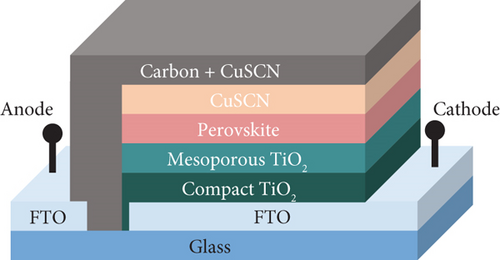
It is essential to consider electron and hole pathways when designing a PSC. Perovskite, as an active material, generates free electrons and holes when exposed to light sources. To utilize them, both free charges need to be separated into the respective charge selective material. TiO2 was selected as the electron selective layer (ESL) because of its excellent transparency due to its wide bandgap and suitable energy level [23]. Moreover, TiO2 has a slightly lower conduction band than perovskite, making it easier to inject photogenerated electrons from the light absorber into the ESL. In this research, the TiO2 layer is composed of compact and mesoporous types. The dense layer acted not only to effectively transfer electrons to the fluoride-doped tin oxide (FTO) layer but also prevented the perovskite absorber from coming into contact with the FTO layer, which can result in recombination and voltage losses. Furthermore, mesoporous TiO2 improves the electron transport properties due to increasing interfacial area. The schematic representation of PSC used in this research is presented in Figure 1.
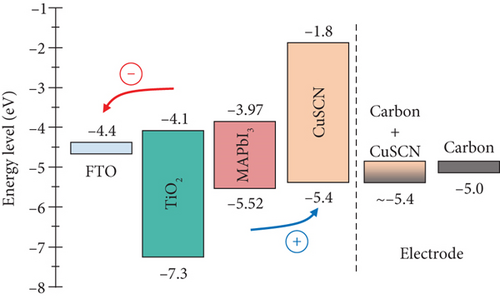
MAPbI3 is used as a light absorber. It has a broad absorption spectrum, a suitable bandgap of 1.55 eV, and ambipolar characteristics. According to a previous report, the valence band and conduction band of perovskite deposited on top of mesoporous TiO2 using a two-step solution are −5.52 and −3.97 eV, respectively [24]. On the other hand, TiO2 has a valence band of −4.1 eV and a conduction band of −7.3 eV, which makes the bandgap of TiO2 3.2 eV [25]. CuSCN was used as both the interlayer and doping material for the carbon electrode. It has a bandgap of 3.6 eV, a valence band of −5.4 eV, and a conduction band of −1.8 eV [26]. On the top layer, carbon was used as a counter electrode and has a work function of 5.0 eV. Employing an additive (CuSCN) into carbon materials adjusts its work function according to the valence band of the additive [18, 27, 28]. Thus, the carbon work function will shift closer to the CuSCN valence band, permitting a more efficient transfer of holes from CuSCN to carbon. A diagram of the device’s energy level is presented in Figure 2.
2.2. Materials and Device Fabrication
FTO glass was purchased from Nippon Sheet Glass. Titanium tetraisopropoxide (TTIP), ethanol, hydrochloric acid (HCl), and chlorobenzene were purchased from Wako Chemicals. Dimethylformamide (DMF), acetylacetone, lead(II) iodide (PbI2), Zn powder, CuSCN powder, and PMMA were purchased from Kanto Chemical. Diethyl sulfide (DES) was provided by Tokyo Chemical Industry. Acetylene black, graphite, and TiO2 paste PST-18NR came from Strem Chemicals, Ito Graphite, and JGC Catalysts and Chemicals, respectively.
The required solutions were prepared before the deposition process. A compact TiO2 precursor solution was made by mixing 0.6 mL of TTIP, 0.4 mL of acetylacetone, and 9 mL of ethanol. Mesoporous TiO2 precursor solution was made by diluting TiO2 paste PST-18NR with a 1:3 mass ratio in ethanol. The perovskite precursor solution was prepared by dissolving 1 M of PbI2 in DMF and then letting the PbI2 dissolve by heating it at 80°C. MAI solution was prepared by dissolving the MAI salts with IPA (10 mg/mL). CuSCN powder was dissolved in DES with a concentration of 35 mg/mL as a CuSCN precursor solution.
The carbon paste was prepared with a 1:1 mass ratio of graphite and acetylene black. Acetylene black was chosen because it has better conductivity than carbon black [29]. The 1:1 ratio was used to balance the characteristics of graphite and acetylene black. Too much acetylene black produces a loose and easily cracked carbon layer, possibly caused by the nanometer-sized acetylene black particles not letting the carbon particles stick firmly together. On the other hand, excess graphite results in gaps in the carbon layer due to its big particle size, preventing proper contact with the layer deposited below. A 10% mass percentage of PMMA to carbon was added into the carbon mixture as a binder. As an additive, 2.5 wt% from the carbon mass of CuSCN powder was added. A chlorobenzene 10 times the mass of carbon was added as a carbon mixture solvent. The carbon paste was stirred at room temperature for at least 1 day to ensure all the carbon and CuSCN were mixed evenly.
The layer-by-layer deposition follows the illustration of Figure 3 and is similar to previously reported literature [30] except for the carbon layer deposition.
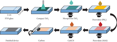
The PSC was prepared outside the glovebox in a room with a relative humidity (RH) of 50%–60%. First, FTO glass was cut into sizes of 2 × 1.25 cm2. Parts of the FTO layer were etched to separate the anode and cathode sections of the solar cell using Zn powder and diluted HCl. Then, the substrate was heated to 550°C in the furnace for cleaning and preparing for the coating of a compact TiO2 layer. The coating was conducted using a spray pyrolysis method. The heated substrate was transferred to a spray chamber, and 2.5 mL of compact TiO2 was sprayed into it. This process was repeated four times where in between sprays, the substrate was heated in the furnace at a temperature of 550°C for 2 min. This was done to ensure the substrate stays heated during the spray process. After the last spray set, the substrate was heated in the furnace at 550°C for 10 min. Then, the procedure continued for mesoporous TiO2 layer deposition after the substrate was left cooled to room temperature. Diluted TiO2 paste was dispersed on the TiO2 compact layer and spun at 4000 rpm for 20 s using a spin coater. The deposited layer was sintered at 550°C for 30 min.
Next, the PbI2 layer was formed on the FTO/TiO2 substrate using the spin coating method. After the PbI2 precursor solution was dispersed, the substrate was spun at 4000 rpm for 20 s, followed by annealing at 80°C for 30 min. To form a compact perovskite layer, the MAI solution was dispersed on the substrate and then spun at 4000 rpm for 10 s. The MAI deposition process was repeated five times, followed by heat treatment at 80°C for 30 min to complete the crystallization process.
After the sample was cooled to room temperature, the CuSCN solution was dispersed into the FTO/TiO2/perovskite substrate, followed by spinning it at 4000 rpm for 20 s. Then, the substrate was heated at 80°C for 15 min to evaporate the CuSCN solvent. Finally, an appropriate amount of carbon paste was placed on the substrate, and a glass rod was rolled to make it into a thin layer. The sample was heated at 80°C for 10 min to evaporate the excess chlorobenzene. A shadow mask with an opening of 0.237 cm2 was added in front of the glass to determine the active area during the current density-voltage (J–V) measurement. PSC without CuSCN interlayer and modified carbon was also developed in a similar manner for comparison. In addition, PSC with Pt electrode was fabricated by stacking a Pt plate on top of the carbon layer and then clipping it to keep it in place with the substrate. This was performed to observe the change in PSC performance on metal-based electrodes.
2.3. Characterization
3. Results and Discussions
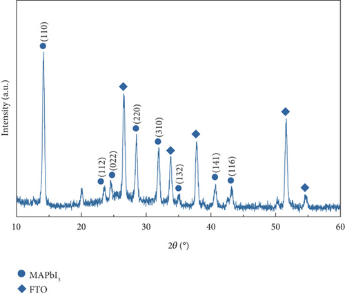
X-ray diffraction (XRD) measurement was conducted to confirm the formation of MAPbI3 perovskite crystal on the PSC. The XRD graph in Figure 4 shows the fundamental MAPbI3 peaks at 2θ of 14.1°, 28.5°, and 32°, which is in good agreement with previously reported literature [35]. The other peaks were for the FTO thin film since the measurement was conducted on the FTO/TiO2/perovskite substrate. The signature peaks of PbI2 at 12.7° were not visible, meaning that the PbI2 layer was completely formed into perovskite and had no sign of perovskite decomposition. However, the characterized substrate contains a TiO2 layer, and the most substantial signature peak of it in 2θ of 25.2° was hardly observed. This might be caused by the mesoporous structure of TiO2, which makes the signature peak weak and buried between the peak of FTO and perovskite [36, 37].
Figures 5(a) and 5(b) provide the SEM cross-section of the PSC showing the carbon layer with and without CuSCN doping, respectively. The thickness of the carbon layer for both conditions is around 30 μm. Morphologically, there is no visible difference between the two carbons. However, the EDS mapping (Figure 5(c)) shows a scatter of sulfur and copper, indicating the presence of CuSCN material on the modified carbon layer. It was noticed that the sulfur and copper signals intensified in the perovskite/carbon interface. This might be caused by the CuSCN settling down on the bottom of the carbon layer during the deposition of carbon paste.

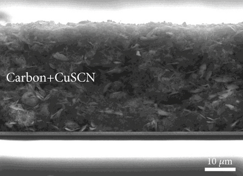

Figure 6 provides cross-section SEM images with a higher magnification to determine the functional layers in the PSCs of various structures. The thickness of TiO2 and perovskite layers is approximately 220 nm, whereas the CuSCN layer is approximately 80 nm. The thicknesses of the perovskite layers for every structure are similar. Therefore, the performance measurement result will depend on adding CuSCN as an HSL and carbon additive.

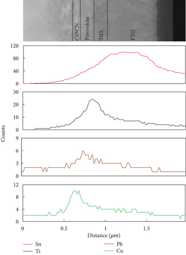
An EDS characterization was carried out to confirm the elements contained in each layer (Figure 7). It was noticed that the element counts of Sn, Ti, Pb, and Cu increased in each designated position. A high Ti element count appeared where the TiO2 layer was deposited, while a high Pb and Cu counts were found for the MAPbI3 and CuSCN layers, respectively. Pb elements appear in the TiO2 area due to TiO2’s mesoporous morphology, letting some diffusion of the perovskite material. These can promote better electron transfer from the perovskite to the TiO2. The element count peak of Cu is seen on the left of the element count peak of Pb, indicating that CuSCN was successfully deposited on top of the perovskite layer.
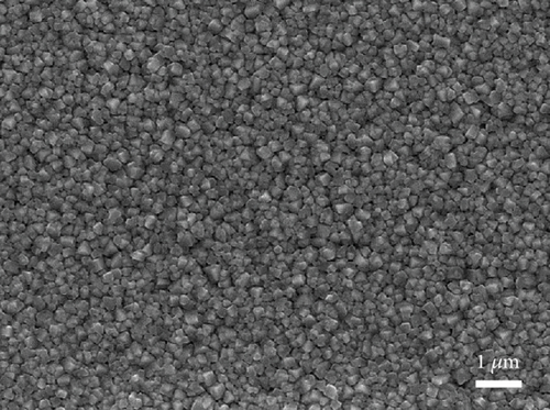
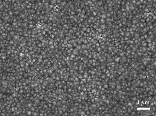
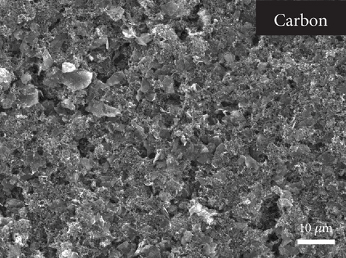
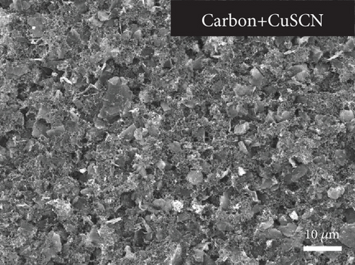
The top view of the SEM image of the perovskite layer can be seen in Figure 8(a). The perovskite layer consists of closely packed cuboid-shaped crystals with a size of 200–300 nm. The small size of the perovskite might come from several factors, such as the use of a single cation of the perovskite compound (i.e., MAPbI3), the deposition method, and the absence of treatment during the deposition process. Additionally, in the two-step deposition method for MAPbI3 perovskite, the crystal size is also dependent on the concentration of the MAI solution [38]. Nevertheless, the grain size of the perovskite is similar to other reported work that creates perovskite layers using a two-step deposition method [39, 40]. Then, the CuSCN layer was also confirmed in Figure 8(b), where the perovskite film becomes blurred due to the thin and low conductivity of the CuSCN film. Figures 8(c) and 8(d) show the carbon layer without and with CuSCN additive, respectively. Again, there is no difference in the morphology of both carbon layers. The irregular particle size in the carbon layer is caused by the large particles of graphite and nanosized particles of acetylene black. From the manufacturer’s technical data sheet, the graphite has an average particle size of 4 μm, whereas the acetylene black is around 42 nm. The combination of both types of carbon is essential in making a carbon electrode. The large-size graphite particle has better conductivity because charge transport happens inside the particle and jumps less from particle to particle. However, the drawback is that it does not efficiently transfer charge from CuSCN to carbon due to gaps in the interface. Therefore, acetylene black, with its nanosized particle, is expected to fill those gaps [41, 42].
After each functional layer of the solar cell had been successfully deposited, the performance of the PSC was measured. Table 1 displays the photovoltaic parameters of PSC with various structures, whereas Figure 9 shows the J–V curve of the PSC. The HSL-free carbon-based PSC possesses the lowest performance with an average efficiency of 0.58%. In contrast, the highest performing structure is when the Pt plate was employed as a counter electrode (stack structure). It was an expected behavior for the Pt-based PSC where the conductivity of the metal electrode is considerably higher than the carbon-based electrode. Subsequently, its RS parameters show the lowest, which is 9.75 Ω·cm2. The reflectivity of the Pt plate also helps the incident light to be reflected to the active material, thus boosting the JSC parameter.
| Structure | VOC(V) | JSC(mA/cm2) | FF | Efficiency (%) | RS(Ω·cm2) | RSh(Ω·cm2) |
|---|---|---|---|---|---|---|
| FTO/TiO2/MAPbI3/carbon | 0.66 ± 0.22 | 3.21 ± 0.55 | 0.27 ± 0.02 | 0.58 ± 0.26 | 76.68 ± 12.9 | 256 ± 115 |
| FTO/TiO2/MAPbI3/carbon + CuSCN | 0.67 ± 0.25 | 4.04 ± 1.87 | 0.29 ± 0.07 | 0.92 ± 0.95 | 73.44 ± 28.26 | 243 ± 114 |
| FTO/TiO2/MAPbI3/CuSCN/carbon | 0.91 ± 0.03 | 10.29 ± 1.33 | 0.48 ± 0.08 | 4.50 ± 1.25 | 17.16 ± 4.92 | 413 ± 207 |
| FTO/TiO2/MAPbI3/CuSCN/carbon + CuSCN | 0.91 ± 0.04 | 10.61 ± 1.68 | 0.52 ± 0.06 | 5.06 ± 1.04 | 13.83 ± 1.91 | 536 ± 210 |
| FTO/TiO2/MAPbI3/CuSCN/carbon + CuSCN/Pt (stack) | 0.91 ± 0.05 | 11.02 ± 1.26 | 0.54 ± 0.08 | 5.31 ± 0.69 | 9.75 ± 1.45 | 441 ± 161 |
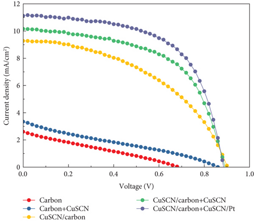
As for the HSL-free carbon-based PSC, the low performance might be caused by the significant gap between the perovskite’s valence band and carbon’s work function. As a result, more energy is lost when the hole passes through from the perovskite interface to the carbon electrode, leading to low VOC [43]. The low value of other parameters, such as JSC and FF, could also be caused by the inefficient minority carrier transfer from perovskite to carbon electrode. There was a slight increase in JSC and FF when CuSCN was added to carbon electrode in HSL-free PSC. This might be due to improved hole extraction caused by more suitable energy level alignment on the perovskite/carbon interface [17].
Nevertheless, the overall performance is low for HSL-free devices. When CuSCN was employed as HSL, the overall performance increased significantly. Since there is no difference in the manufacturing of the TiO2/perovskite layer, it can indicate that the CuSCN interlayer contributes to a more efficient charge transfer. The performance further improved when the CuSCN was added to the carbon, and the efficiency increased from 4.50% to 5.06% for the CuSCN/carbon and CuSCN/carbon + CuSCN structure, respectively. That efficiency boost is contributed by an elevated FF value through the improvement of RS and RSh parameters. The steady-state PL spectra shown in Figure 10 further explain the performance enhancement in the sample that utilizes CuSCN material.
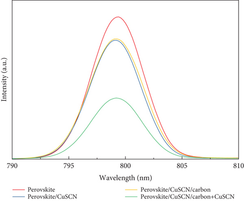
The steady-state PL spectra were obtained by exposing the sample with a 532 nm laser beam. As the sample is exposed to the light, the electrons in the material move into excited states. Electrons are then expected to return to equilibrium while emitting photons with specific wavelengths. In this measurement, an intense photon emission was observed around the wavelength of 799 nm. All samples produce similar peak wavelengths, meaning there is no bandgap change when the HSL or carbon is added to the perovskite [44]. However, when CuSCN was added on top of the perovskite layer, the PL intensity decreased. This is attributed to a rapid hole extraction in the perovskite/CuSCN interface (i.e., the recombination is suppressed, leading to less photon emission). On the other hand, the PL intensity from the perovskite sample with a bare carbon layer is not significantly different from the perovskite/CuSCN sample, implying no improvement in the charge extraction. This indicates that bare carbon has no significant influence in improving charge extraction. Samples with CuSCN HSL and modified carbon further quench the PL intensity, meaning photogenerated charge carrier extraction happens more efficiently than the former configuration. These findings show that utilizing CuSCN as both an HSL and carbon electrode additive provides a significant improvement in charge transfer and was translated to excellent photovoltaic performance among other studied structures.
The EIS measurement was performed to study the interfacial charge transport and recombination. The measurement from low to high frequency produces a semicircle when plotted on the Nyquist plot, as shown in Figure 11. These can be interpreted into equivalent circuits (inset of Figure 11), and various resistance values can be obtained by fitting the Nyquist plot, as summarized in Table 2. RSeries corresponds to the intrinsic series resistance of the solar cell, RCT is charge transfer on the perovskite absorber, and Rrec are associated with the charge recombination process in the device [45–47]. The Rrec value was derived to be 104 and 280 Ω for PSC with bare carbon electrode and modified carbon electrode, respectively. Since the structure was identical in these two devices (FTO/TiO2/MAPbI3/CuSCN), the measurement result suggests that PSC with a modified carbon electrode can suppress the recombination better. On the other hand, the RCT value on the modified carbon electrode is lower (112 Ω) than the conventional one (265 Ω). This indicates that CuSCN inside the carbon electrode has a positive impact on charge transport. The EIS characterizations are in good agreement with PL measurement and can explain the improvement in the photovoltaic parameters.
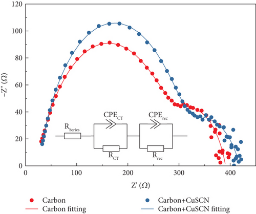
| Electrode | RSeries(Ω) | RCT(Ω) | Rrec(Ω) |
|---|---|---|---|
| Carbon | 23 | 265 | 104 |
| Carbon + CuSCN | 26 | 112 | 280 |
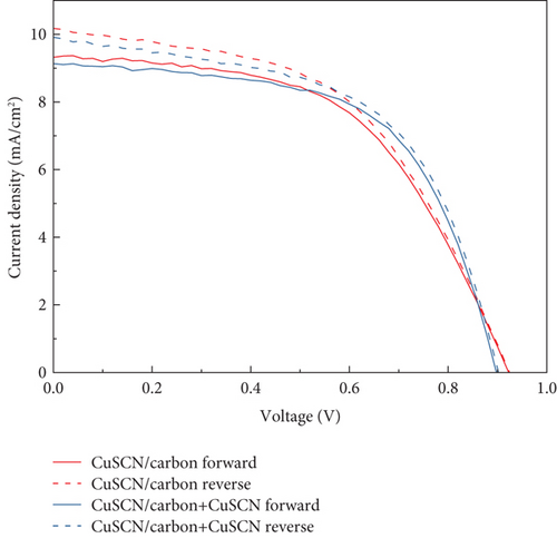
ƞfwd and ƞrev are the efficiencies measured under forward and reverse scan direction, respectively. Figure 12 displays the J–V curve of PSCs with bare carbon and modified carbon measured under forward and reverse scans. There is a visible difference in JSC value between forward and reverse scans. This phenomenon might be related to the capacitive current during the forward and reverse scan [38, 49]. In the PSC, voltage changes during J–V measurement generate capacitive current, resulting in different current readings depending on the scan direction. In the case of a forward scan, the photogenerated current is stored as a capacitive charge and cannot be released to an external load. In contrast, during the reverse scan, the capacitive charge is discharged along with the photogenerated current. These factors lead to an underestimation of current during the forward scan and an overestimation of current during the reverse scan before reaching the steady-state current. However, hysteresis is affected not only by the scan direction. The main cause of hysteresis in PSC is still under debate among researchers. Several studies also suggest that it arises from the ferroelectric effect in perovskite, unbalanced charge transport, trap-assisted charge recombination, and ion migration [50]. The reduced HI (Table 3) in PSC with CuSCN HSL and modified carbon may come from reduced photogenerated charge recombination and charge extraction improvements due to the employment of CuSCN material in two places.
| Structure | HI |
|---|---|
| FTO/TiO2/MAPbI3/CuSCN/carbon | 0.039 |
| FTO/TiO2/MAPbI3/CuSCN/carbon + CuSCN | 0.013 |
The relatively low performance of PSC might be caused by the humidity in the processing area. In this research, PSC was fabricated outside a glove box. It is widely known that perovskite material is susceptible to water, including moisture in the air. The use of basic MAPbI3 perovskite can also be a factor in the lower performance compared to other carbon-based PSCs, which usually use multication perovskite [51]. However, the performance of PSC in this research is comparable to that of other publications that use MAPbI3 perovskite and processed in ambient conditions. On top of that, several publications also still utilize organic HSL and metal counter electrodes on their structure. Table 4 summarizes works related to PSC, which were developed on ambient conditions with similar RH to this research.
| RH (%) | Structure | Efficiency (%) | Ref. |
|---|---|---|---|
| 50–60 | FTO/c-TiO2/m-TiO2/MAPbI3/CuSCN/carbon + CuSCN | 5.06 | This work |
| 50 | FTO/c-TiO2/m-TiO2/MAPbI3 + TEOS/spiro/Ag | 8.60 | [52] |
| 50 | FTO/c-TiO2/m-TiO2/MAPbI3 + tBP/spiro/Ag | 12.60 | [53] |
| 50–60 | FTO/c-TIO2/m-TiO2/MAPbI3/spiro/Ag | 4.30 | [40] |
| Air | FTO/c-TiO2/m-TiO2/MAPbI3/PTSA/CuInS2/carbon | 10.66 | [54] |
- Abbreviations: Air: ambient air (RH not stated); PTSA: p-toluenesulfonamide; Spiro: spiro-OMeTAD; tBP: 4-tert-butylpyridine; TEOS: tetraethyl orthosilicate.
4. Conclusions
In conclusion, we investigated the use of CuSCN as an interlayer in the perovskite/carbon interface and a carbon electrode additive on carbon-based PSCs. This work utilized CuSCN through a combination of two strategies that had only been studied separately before. The influence of CuSCN as an HSL, a carbon additive, or both on the performance of carbon-based PSCs was evaluated and compared. Utilizing both strategies led to a substantial performance improvement for carbon-based PSCs compared to that employed CuSCN only as an interlayer or a carbon additive. The J–V characteristic curves revealed that using CuSCN as both HSL and carbon additive improves the efficiency of carbon-based PSC from 0.58% to 5.06%. Improvement in photovoltaic parameters was attributed to enhanced charge transfer. This can be confirmed further by having the lowest photon emissions in PL measurement, the highest recombination resistance, and the lowest charge transfer resistance in EIS characterization. The proposed structure is expected to pave a new path for further improving carbon-based PSC performance. It also facilitates the commercialization of carbon-based PSCs since all the solar cells were fabricated under ambient conditions, and the device architecture can be easily upscaled.
Conflicts of Interest
The authors declare no conflicts of interest.
Funding
This work was supported by Directorate General of Higher Education, Research and Technology, Ministry of Education, Culture, Research and Technology, Republic of Indonesia, through Doctoral Dissertation Research (PDD) funding (Grant No. NKB 912/UN2.RST/HKP.05.00/2023) and from the Faculty of Engineering, Universitas Indonesia, through Professor Seed Funding (Grant No. NKB 1953/UN2.F4.D/PPM.00.00/2022).
Acknowledgments
This work was supported by Directorate General of Higher Education, Research and Technology, Ministry of Education, Culture, Research and Technology, Republic of Indonesia, through Doctoral Dissertation Research (PDD) funding (Grant No. NKB 912/UN2.RST/HKP.05.00/2023) and by the Faculty of Engineering, Universitas Indonesia, through Professor Seed Funding (Grant No. NKB 1953/UN2.F4.D/PPM.00.00/2022).
Open Research
Data Availability Statement
The data that support the findings of this study are available from the corresponding author upon reasonable request.


