Thermal Analysis of a Plasmonic Perovskite Solar Cell: Using Coupled Opto-Electro-Thermal (OET) Modeling
Abstract
Organic-inorganic heterojunction perovskite solar cells (PSCs) are of high interest due to their low manufacturing cost and higher power conversion efficiency (PCE). Hence, we study the opto-electro-thermal (OET) characteristics and investigate the optical and carrier transport and thermodynamic behaviors on the PSC. In this research, optical and electrical coupled behavior is investigated, and the results of this simulation are in the optimal state for nanoparticles (NPs) with a diameter of 50 nm: the short-circuit current (Jsc) of 18.05 mA/cm2, the open-circuit voltage (Voc) of 0.9406 V, and PCE of 14.15% were obtained. Then, by adding thermal behavior to optical and electrical physics, thermal effects and power losses in the solar cell were obtained. In this case, 221.5 W/m2 Joule heat, 154 W/m2 thermal heat, 123 W/m2 Peltier heat, and 92.3 W/m2 nonradiative heat waste power were achieved. Under these losses, the electrical parameters decrease. The parameters are Jsc = 21.74 mA/cm2, Voc = 0.94 V, and PCE = 13.53%. The best case is obtained for the structure without NPs.
1. Introduction
Today, with the progress of humans in various fields, dependence and necessity for energy is increasing more and more due to its high demand. This energy demand has been shown in different ways [1–5]. In recent years, a new generation of solar cells called perovskite solar cells (PSCs) has been able to occupy a special place compared to new generations of solar cells, so that the power conversion efficiency (PCE) of these solar cells has increased from 3% to 23% in a short period [6–12]. These cells have been noticed due to relatively simple and cheap construction as well as high PCE. Another advantage of these cells over previous generation of solar cells is that they respond to sunlight at more wavelengths, which causes high carrier mobility, high open-circuit voltage (Voc), and long emission length [13–20]. For this reason, researchers are looking for PSCs to obtain more profit in solar cells [21–25]. One of these ways is to utilize the plasmonic effects of metal nanoparticles (NPs) in the structure of solar cell for increasing the PCE value [26–28]. Noble nanometals such as gold (Au), silver (Ag), and copper (Cu) have been considered due to their high plasmon resonance in the visible region [29]. By using them, the absorption capacity of light is increased, which increases the energy generation in the system and increases the PCE in the cell. To increase the PCE value, the short-circuit current (Jsc) and Voc should be increased, where for optimizing the value of Jsc, the carrier generation rate can be increased and the recombination rate of the system can be reduced, which this has a direct effect on Jsc. In order to increase the rate of carrier generation, the amount of the absorption layer (i.e., perovskite) can be increased, which, in addition to increase the manufacturing cost [30–32], causes the carriers generated in the active layer (AL) to recombine before reaching the lower metal contact due to the lengthening of the diffusion path and increase the recombination [33–35]. For this purpose, to reduce the cost and increase the PCE, researchers use metal NPs, which this reduces the thickness of the AL, while the PCE of the cell does not decrease [36]. With the presence of metal NPsin the AL, the amount of electric field in this layer and absorption increases. Naturally, the generation rate decreases, but the presence of metal NPs and the increase of the electrical field in the AL compensate for this decrease in absorption and generation. There is another method to reduce the cost and improve the PCE by trapping the light, which allows the PSC structure to absorb sunlight with an AL thinner than the intrinsic absorption length of the material. It reduces the thickness of the perovskite layer and thus reduces the cost of cell manufacturing. Also, light trapping improves the cell PCE because a thinner cell increases the value of Voc due to the creation of better optical charge carriers [37]. In plasmonic structures, using metal NPs such as Au, Ag, and Cu and creating surface plasmon resonance (SPR), they absorb and trap more sunlight. LSPR excitation and its characteristics are affected by electrical properties, dimensions, shape, and temperature properties of NPs as well as the dielectric material around them [38–41]. Increasing the distance from the surface of metal NPs decreases the amount of electromagnetic field, which in this process increases the electromagnetic field due to radiation effects and the scattering of light in the near field and far field [42–45]. In the near field, by coupling the plasmonic dipole field and the dipole field of the AL, they increase the interaction of light and materials together and enhance the electric field around the NP [46, 47]. The stability of PSCs can be influenced by the addition of plasmonic NPs. The incorporation of plasmonic NPs in perovskite materials can influence various factors such as electrical conductivity, surface roughness, perovskite crystal quality, and surface passivation, all of which are crucial for the PCE and stability of PSCs [48]. Plasmonic NPs can enhance the optical and electrical characteristics of PSCs, leading to improve device performance and stability [49, 50]. Additionally, the presence of plasmonic NPs may favor the chemical stability of the perovskite material, further contributing to the stability of the solar cells [29]. Therefore, the addition of plasmonic NPs holds promise for enhancing the PCE and stability of PSCs.
Among the features of surface plasmonic NPs, we can mention the enhancement of absorption and scattering and the increase of the electromagnetic field to facilitate the transport of the carrier to improve the electrical properties [51]. As we know, the perovskite (CH3NH3PbI3) absorption range is less than 650 nanometers; that is why we use plasmonic NPs to improve the absorption in infrared wavelengths near the sun’s spectrum [52, 53]. In one of the studies, the amount of plasmon in the AL can be adjusted by changing the size, geometry, location, and type of material, and the plasmon in the wavelengths of 650 to 800 nm, which we had a loss in the AL, was increased by metal NPs [54–56]. The change in the plasmonic properties of Ag is due to the favorable conditions in its metal oxidation [57].
In the past years, the PCE in PSCs has reached 25%. Perovskite light absorbers have unique advantages, including high absorption coefficient, long carrier emission length, and low exciton binding energy [58–60]; the intrinsic (or lightly doped) perovskite layer is sandwiched between the hole transport layer (HTL) and the electron transport layer (ETL) so that a pair of heterojunctions is formed, which ensures the separation and efficient transport of photocarriers. In SCs, there are important thermal effects and losses in the system that lead to an increase in the cell temperature and affect the stability of the cell. Among the thermal losses can be heating, Joule, and Peltier heat, which causes a decrease in stability in the system [57, 61–63].
Recently, 3D simulation platforms have been presented with detailed models that can couple optical-electrical-thermal modules. Although solar cells are thermodynamic devices, the heat generation and dissipation mechanisms in these devices have rarely been investigated, specifically through modeling or simulation analysis. Also, in solar cells, the heat in the cell itself can be heated and affect the PCE of the cell, including this thermal heat can refer to self-heating and heating from light [64, 65]. In solar cells, a large part of the sun’s energy absorbed by the cell is converted into heat in various ways, increasing the cell temperature and reducing the cell’s PCE [8]. So, thermal losses play a significant role in the operation of solar cells, which have been rarely examined in the articles. Therefore, photovoltaic solar cells are also conventional thermodynamic systems in addition to optical and electrical systems [66, 67]. In previous studies, the working conditions of ideal cells were mainly assumed (air mass index 1.5, solar radiation Ps = 1000 W/m2, and ambient temperature Tamb = 25°C), and it was assumed that the operating temperature of the cells (T) is equal to Tamb [67, 68]. On the other hand, when the solar cell is exposed to sunlight, the temperature of the cell increases, and it affects the PCE of the cell. In this model of research, Maxwell’s equations are used to perform optical studies counting absorption, generation, and transfer of reflection carriers. Then, we obtain the different mechanisms of surface and mass recombination and carrier diffusion caused by the carrier concentration gradient, examine the cell electrically, and calculate and examine the cell temperature. All the energy absorbed in the solar cells cannot be used in the electrical part of the structure, because in the system, part of this energy is converted into heat (Joule heat, Peltier heat, etc.) or in the form of photons through optical recombination and it will be wasted. After the optical and electrical investigations, solar cells are thermodynamically analyzed, including heat generation (due to heating, Joule heat, Peltier heat, and recombination heat) and heat loss (such as convective and radiative cooling) [69]. In the previous articles, attempts were made to investigate optical and electrical physics, but in some paper, reports about the OET system have also been reported. In recent years, opto-electro-thermal (OET) modeling has been investigated in some studies, in which radiation cooling technology has been investigated in the effective cooling of systems. In this model, a silicon-based (SC) radiative cooling solar cell was investigated (OET), in which the effects of radiative cooling, thermodynamic and electrodynamic behaviors of carriers, temperature effects, and physical and thermodynamic analysis parameters were investigated. In this model, solar cells with radiation cooling and without radiation cooling have been compared, which shows that the temperature of the silicon-based solar cell can decrease to 10%, and for this reason, the PCE of the solar cells can be increased by 0.45% [69, 70].
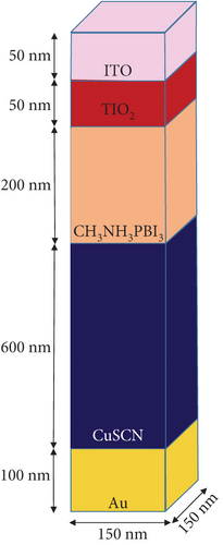
Figure 1 shows the simulation structure which has been optimized in recently reported work [13] in which the top interface is indium tin oxide (ITO) with a thickness of 50 nm. An ETL of titanium dioxide (TiO2) with a thickness of 50 nm, an AL of perovskite (CH3NH3PbI3) with a thickness of 200 nm, an HTL of copper thiocyanate (CuSCN) with a thickness of 600 nm, a bottom metal interface made of gold (Au) with a thickness of 100 nm, and a metal (Ag) NP with the diameters of 5 to 100 nm in the middle of the AL are formed. TiO2 has a suitable energy band, and the process of manufacturing and layering is easier in it. Also, this material reduces recombination and increases shunt resistance and acts as a hole-blocking layer [70–72].The AL of this structure consists of perovskite (CH3NH3PbI3), which has easier manufacturing and synthesis, higher PCE, lower production cost, high absorption of the sunlight spectrum, stability of the energy band, and more carrier emission. The HTL is made of a structure consisting of copper thiocyanate (CuSCN), which is an inexpensive mineral. Other features of this material include better hole transport, a large bandgap, and an easier manufacturing and synthesis process. The matching of its energy levels with perovskite reduces carrier recombination and improves carrier extraction, thus improving the fill factor (FF) and the PCE in a solar cell [73].

In this work, we must obtain the results of optical, electrical and thermal simulations through finite element method (FEM). Our simulation is done in three parts: optical, electrical and thermal. The material parameters for simulation are given in Table 1 [74, 75]. The optical part is used to find the absorption, reflection, and transmission parameters obtained by obtaining the distribution of the electromagnetic field through the solution of Maxwell’s equations. Then, using the obtained results, the electrical part of the solar cell is obtained, which is solved in the electrical theory of the coupled electron/hole transport equations and the Poisson equation for the electrostatic potential. In the thermal part, the thermodynamic equations of the carrier and thermal diffusion or generation processes and macroscopic heat loss are obtained through heat diffusion equations under the principle of conservation of energy.
| Parameter | TiO2 | CuSCN | CH3NH3PbI3 |
|---|---|---|---|
| εr | 9 | 10 | 6.5 |
| NC (cm-3) | 1 × 10¹⁹ | 1.79 × 10¹⁹ | 1.66 × 10¹⁹ |
| Nv (cm-3) | 1 × 10¹⁹ | 2.51 × 10¹⁹ | 5.41 × 10¹⁹ |
| μn/μp (cm2/V·s) | 20/10 | 25/25 | 50/50 |
| X (eV) | 4 | 1.9 | 3.93 |
| Eg (eV) | 3.2 | 3.4 | 1.55 |
| NA (cm-3) | — | 5 × 10¹⁸ | 5 × 10¹³ |
| ND (cm-3) | 5 × 10¹⁸ | — | — |
| τn/τp (ns) | 5/2 | 5/5 | 8/8 |
| Nt (cm-3) | 1 × 10¹⁵ | 1 × 10¹⁴ | 1 × 10¹¹-1017 |
| An/Ap | — | — | 2.85786 × 10⁻²⁶ |
| B | — | — | 2.82 × 10⁻⁹ |
The maximum energy of sunlight in a vacuum is 300 nm. In these solar cells, light absorption reaches zero after the wavelength of 800 nm because the bandgap of perovskite material is equal to 1.55 eV; in a result, the input light power will be Am1.5, and our simulation spectrum is in the range of 300 to 800 nm.
1.1. Plasmon
May’s theory can be used in analyzing the behavior of metal NPs exposed to sunlight. When the NPs are small, the field is created a little around them. But while the large NPs fall into the AL, the lights are scattered in different directions after colliding with the NPs [76].
In this equation, εp is the particle dielectric function, V is the volume of the particle, and εm is the dielectric function of the embedding medium. It can be seen that the particle polarization becomes very large when εp = −2εm. It is known as the exacerbation of the surface plasmon resonance (SPR). In SPR, the cross-sectional cross-section can exceed the geometric cross-section of the particle [77].
1.2. OET Theory
Now we examine thermal physics. To solve the equations in the thermal state, we add the thermodynamics to the structure, but should note that the optical, electrical and thermal responses are examined simultaneously. After solving the Maxwell equations for the optical part and using them as inputs to the electrical part, also solving the Poisson equations, we can obtain the electron/hole transport characteristics. For thermal physics, carrier thermodynamic equations and simultaneous heat emissions must now be dissolved to calculate the energy absorption of carrier heat and relaxation under the principle of energy survival. The purpose of calculating the losses in this work is to bring the simulation results closer to reality and find destructive factors in the cell PCE.
Table 2 shows the thermal parameters related to different parts of the solar cell structure used for the simulation [78–80].
| Parameter | ITO | TiO2 | CH3NH3PbI3 | CuSCN | Au |
|---|---|---|---|---|---|
| ρ | 5560 | 3900 | 4286.4 | 2840 | 19300 |
| K | 31 | 4.8 | 0.59 | 2.39 | 129 |
| Cm | 128 | 683 | 308 | 800 | 318 |
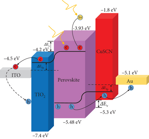
As we know, the carrier transfer equations are temperature-dependent because the network temperature gradient acts as an additional force to move the carriers. The diagram in Figure 2 shows the schematic of microscopic processes in photovoltaic systems and the energy band in SCs, where the incident photons deliver energy to the carriers and release light current and heat.
1.3. Heat Producing Factors
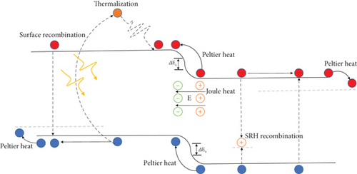
In this work, after performing optical calculations and obtaining its parameters with the help of the electrical model, we take the current-voltage characteristics, and by pairing it with the thermal module, we obtain the thermal losses. Figure 3 shows the heat generation factors in the system and how heat is released; in the following, we will examine each one separately.
- (i)
Thermalization: when the energy of the incoming photon is greater than the bandgap, hot electrons are generated in the conduction band (created by hot photons (hv > Eg)); due to creating their instability at this level, they tend to reach stability, that is why the electrons, the hot ones, come down from the edge of the conduction band and release their energy in the form of heat.
- (ii)
Joule heat (HJoule): which is generated due to the movement of carriers under the electric field and the flow of light in the discharge area where the electric field is strong:
- (iii)
Nonradiative recombination heat (Hnon-rad): which is obtained from the sum of nonradiative recombination such as the SRH recombination and Augur recombination. Nonradiative recombination generates heat after electron recombination to midgap defects and energy exchange between carriers, respectively.
- (iv)
Surface recombination: which occurs due to heat generation on the surface of traps/defects due to recombination:
- (v)
Peltier heat: it occurs when electrons (holes) fall from the conduction band (valence band) to the quasi-Fermi surface before being collected by the external circuit, producing heat.
| Thermalized heat | Joule heat | Peltier heat | Total recombination heat | |
|---|---|---|---|---|
| Power density (W/m2) | 131.9 | 37.05 | 83.23 | 16.79 |
To validate this work with past articles, the simulation results in past articles are given in Tables 4 and 5 [50, 57, 69, 77].
1.4. Heat Dissipation Pathways
1.5. Simulation Procedure
Our simulations consist of two stages; in the first stage, optical simulations are performed to obtain the light generation rate (Gtot) that is used as input for the electrical module to provide the current-voltage (I-V) characteristics, as well as the temperature of the semiconductor. At this stage, the PSC is optimized by changing the NP radiation and the effect of plasmonic effects. When the Ag NP with a radius of 25 nm is located in the AL, the PCE has the highest value. In the second stage, the temperature distribution calculated in the coupled modules of the first stage is calculated.
2. Results and Discussion
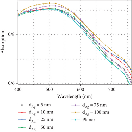
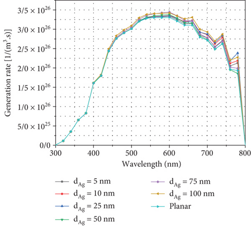
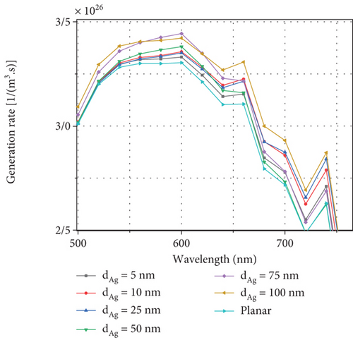
Figure 4 shows the absorption diagrams and generation profiles in the solar cell for wavelengths from 300 to 800 nm. The absorption diagram is shown in Figures 4(a) and 4(b), and the generation rate is demonstrated in Figures 4(c) and 4(d) for wavelengths from 300 to 800 nm in the structure. At wavelengths around 300 nm, more incident light is generated by the ITO and TiO2 layers. As the wavelength increases, the absorption rates in these two layers will be decreased, where the AL (CH3NH3PbI3) absorbs light at wavelengths between 300 and 800 nm. At the same time, from 550 nm onwards, the amount of absorption in this layer gradually decreases, and at the wavelength of about 750, this decrease becomes more intense.
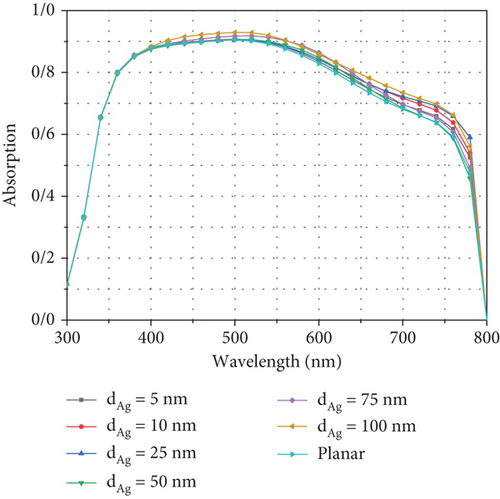
We experience a decrease in absorption in the perovskite layer at wavelengths of 550 nm, and later, the CuSCN layer begins to absorb light, but because this layer cannot generatecarriers, it does not affect the current characteristics.
One of the ways to increase the absorption in the AL is the use of metal NPs and plasmonic stimulation. In this article, we are trying to improve the absorption in this layer by adding NPs to the perovskite layer continuously and periodically. We placed Ag NPs with different diameters in the perovskite layer and investigated the effect of absorption and generation. We know that the Ag plasmon is in the wavelength region of 500 nm, so according to Figures 4(a) and 4(b), with the increase in the diameter of the Ag NPs, the number of absorptions increases from the region of about 550 to 650 nm. In addition, nanostructures cause a change in the electric field in the cell, somehow that of the incoming light, after hitting the NP that scatters the light in different directions and increases its movement path in the active area and increases absorption. For this reason, this causes the light at higher wavelengths, which have less energy, to go to the lower layer, i.e., CuSCN, and also increases the field in the AL, and therefore, the absorption of light for wavelengths of 550 nm and later increases compared to the planar state. For wavelengths of 700 nm and later, due to the reduction of the field and the reduction of the carrier generation, the amount of absorption in the cell decreases drastically. Figures 4(c) and 4(d) show the generation rate in the system. Because the field and absorption factor have a direct effect on the generation rate equations, for this reason, the behavior of the generation rate for different wavelengths will be the same as absorption so that at low wavelengths with high energy, the light incident on the cell is absorbed by the ITO and TiO2 layers. As the wavelength increases and the energy decreases, the absorption of the first two layers decreases, and the absorption in the perovskite AL (MAPI3) increases in wavelengths longer than 550 nm due to the plasmon phenomenon and the presence of Ag NPs; the generation rate increases. As can be seen, like absorption at wavelengths higher than 700 nm, the generation rate decreases drastically due to the reduction of the field in the recite layer.
Figure 5(a) shows the diagram of the electric field in the PSC structure with Ag NPs with the diameter of 50 nm at wavelengths of 400, 600, 500, and 800 nm. As the wavelength of light entering the PSC increases and approaches the Ag plasmonic wavelength, the plasmon electric field increases in the AL and around the NP, which improves absorption and generation in this wavelength, according to Figure 5.
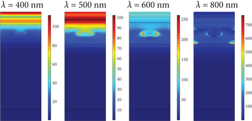
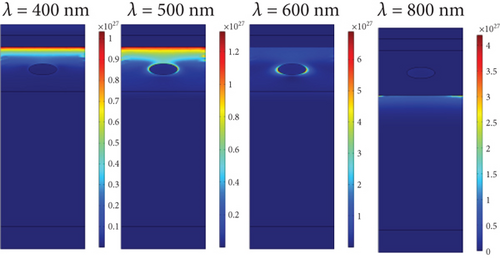
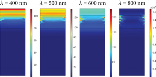
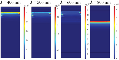
Figure 5(b) shows the generation rate diagram in the PSC with Ag NPs with the diameter of 50 nm at wavelengths 400, 600, 500, and 800 nm. By increasing the wavelength of the light entering the cell and approaching the Ag plasmonic wavelength, the electron-hole generation rate in the AL and around the plasmonic NP increases, which, according to Figure 5, leads to an improvement in the generation rate at this wavelength.
Figure 5(c) shows the electric field distribution in the PSC structure without Ag NPs at wavelengths 400, 600, 500, and 800 nm. At higher wavelengths, the amount of absorption improves due to increased light transmission in the upper layers of perovskite. Figure 5(d) shows the distribution of the generation rate in the solar cell without Ag NPs at wavelengths 400, 600, 500, and 800 nm.
At higher wavelengths, due to increased absorption, the generation speed improves. The distribution of the electric field at the wavelength of 500 nm is shown for the planar state, where the distribution of the electric field in the ITO and TiO2 layers is greater than that of perovskite. It means that the perovskite layer absorbs the generated field, and according to the shape of the absorption rate in the cell, it has the highest value compared to other wavelengths. In this regard, Figure 5(d) shows the generation rate at a wavelength of 500 nm.
ITO and TiO2 layers cannot produce carriers; that is why the generation rate in this layer is zero, but in the AL, due to the increased absorption and generation of electron-hole carriers, the generation rate has increased compared to the two higher layers. Figure 5(a) shows the profile of the electric field when we place a Ag NP with the diameter of 50 nm right in the center of the perovskite layer.
This figure shows that the Ag plasmon caused the field around the NP to increase significantly compared to the planar structure, and this, according to Figures 5(a) and 5(b), shows that the absorption rate and the generation rate compared to the planar structure during different waves have increased. Figure 5(c) also shows the profile of the generation rate when the 50 nm Ag NP is in the center of the AL, which shows that the generation rate has increased in this state compared to the planar structure.
Figure 6(a) shows the diagram of the dark current in the system, that is, when there is no carrier in the solar cells and light does not enter the solar cell. The dark current represents the amount of recombination in the system, so that by adding Ag NPs to the perovskite layer and increasing its diameter from 2.5 to 50 nm,the recombination increases according to the dark current diagram. Increasing the amount of recombination in the system reduces Voc and Jsc because recombination is directly related to the resistance of the AL. Therefore, it can be concluded that the presence of metal NPs sometimes causes damage to the cell. Figure 6(b) shows the recombination rate diagram in the system at wavelengths of 300 to 800 nm. From 2.5 to 50 nm, it can be seen that it increases with the recombination rate. When the light enters the active area, as the diameter of the NP increases, the amount of light hitting the NP increases and causes more light to scatter in unusual directions in the perovskite layer and the length. The increased light path, therefore, increases the amount of carrier absorption and generation. With the increase in carrier generation, the recombination ratio also increases.
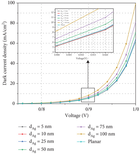
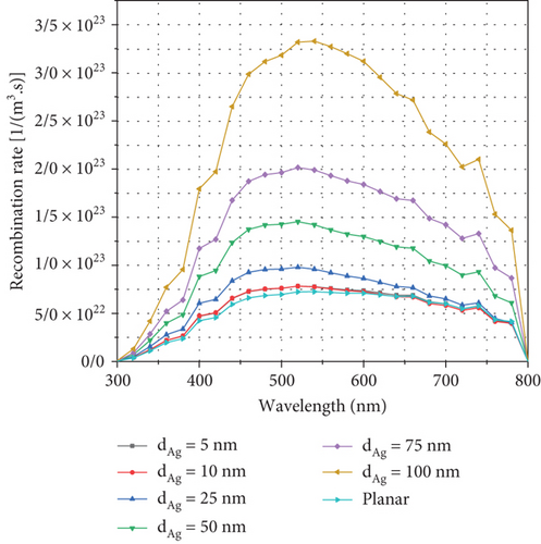
Figure 7(a) shows the current density versus voltage plot for the solar cell, showing the behavior of Voc and Jsc for the planar structure and when we put NPs of different diameters in the middle of the perovskite layer. Figure 7(b) shows the changes in Voc behavior with the addition of NPs in the AL, which increases the resistance and creates defects in the perovskite layer, which causes hardening and increases the resistance in the transport of carriers in the AL.
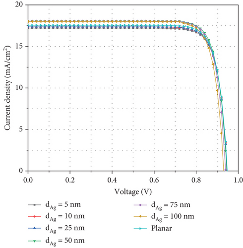
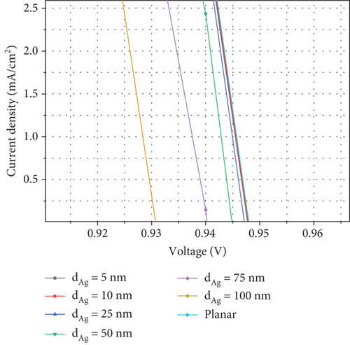
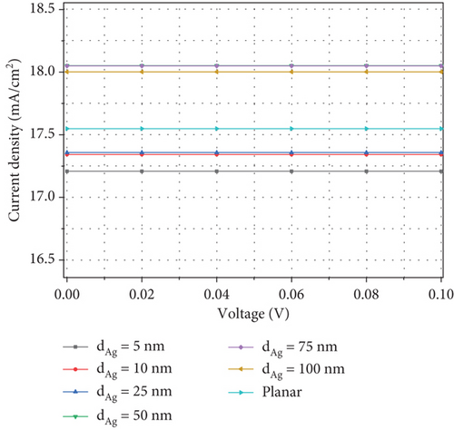
The behavior of Voc is directly related to Jsc and the current recombination density (J0) so that Voc = (kT/q) ln (Jsc/J0 + 1), where k is the Boltzmann constant, T is the temperature, and q is the charge of electrons. Therefore, according to the small changes of Jsc, Voc indicates the recombination in the system. With the increase of recombination in the solar cell according to Figure 7(b), the value of Voc in the planar structure is slightly less than 0.95 V, which by adding Ag NPs to the perovskite layer and increasing the diameter of Voc to 0.93 V decreases. Figure 7(c) also shows the behavior of Jsc in the system, which according to Eq. (6) depends on the compromise between the generation and recombination rates. As shown in this figure, with the addition of NPs to the system, the current begins to increase from 5 nm and continues up to when the diameter of NP reaches 75 nm. But from this diameter onwards, due to the preponderance of recombination rate, the increase in current is reduced. However, Jsc decreases when the diameter of NP is 100 nm compared to when the diameter is 75 nm.
Table 6 shows the changing trend of PCE, FF, Voc, and Jsc, for various values of Ag NP diameter placing in the AL. As is known, the PCE behavior is affected by the current and voltage values. Based on these results, the best performance in the solar energy of this cell occurs when the Ag NP with the diameter of 50 nm is placed in the perovskite layer, which has increased the PCE of PSC by 2.64% compared to the planar structure. The overall behavior of the FF is similar to Voc and is affected by the recombination behavior in the system.
| PCE (%) | FF (%) | Voc (V) | Jsc (mA/cm2) | |
|---|---|---|---|---|
| Planar | 13.789 | 82.39 | 0.9480 | 17.54843 |
| dAg = 5 nm | 13.532 | 82.47 | 0.9478 | 17.20868 |
| dAg = 10 nm | 13.644 | 82.5 | 0.9478 | 17.34264 |
| dAg = 25 nm | 13.65 | 82.53 | 0.9472 | 17.35771 |
| dAg = 50 nm | 14.1537 | 82.49 | 0.9447 | 18.05188 |
| dAg = 75 nm | 14.0435 | 82.22 | 0.9406 | 18.04917 |
| dAg = 100 nm | 13.8525 | 79.53 | 0.9307 | 18.00173 |
2.1. Heat
In practice and construction, we have effects such as recombination and temperature effects in the system, which affect the PCE and consequently the performance of the cell, while they are less considered in the simulations. In this article, we tried to simulate solar cells by considering the actual effects and bringing them closer to reality. In the last part, the results of the optical and electrical simulations were calculated in the standard mode, which included SRH recombination. The thermal analysis is performed along with the addition of new physics to the simulation. Consider that adding thermal physics to the simulation structure as well as temperature effects has a negligible effect on the refractive index of the material and the real and imaginary parts. This means that the addition of this physics does not affect the optical analysis and the generation and absorption rates in the cell. For this reason, we give up the optical analysis in thermal physics and consider them according to the previous analysis.
Figure 8 shows the dark current-voltage plot for the planar structure with Ag NPs of different diameters in thermally coupled physics. The dark current indicates the amounts of recombination rate and Voc in the system, so here due to the increase in the recombination rate and the calculation of radiative and nonradiative recombination of the dark current compared to the previous case where only SRH recombination was calculated (as shown in Figure 4), attention has increased. An increase in the recombination rate in a solar cell reduces the value of Voc, which this in turn reduces the PCE of the cell.

Figure 9 shows the graph of current density in terms of voltage, which shows the change in the behavior of Voc and Jsc for the planar structure and when we put NPs of different diameters in the middle of the perovskite layer. Manufacturing and recombination parameters affect the value of Jsc. Therefore, with the stability of the generation rate compared to the state and the increase of the recombination rate in the system, we see a significant decrease in Jsc for increasing the NP diameter. Furthermore, this increase in recombination has led to a reduction in Voc. When we start adding silver NPs to the structure, with the increase in diameter, it becomes harder to transport the carriers, and it causes an increase in the resistance in the cell in addition to Voc, which reduces Jsc.
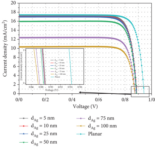
Table 7 shows the variations of electrical parameters, i.e., PCE, FF, Voc, and Jsc, for various values of Ag NP diameter. The thermal physics is coupled to the system, as well as the effect of temperature and optical and nonradiative recombination in the system both in the planar structure and when Ag NPs with different diameters are added to the AL. As a result, we see a decrease in the PCE, so the profit from 13.53% in the planar state reaches about 7.51% when we have NPs with a diameter of 100 nm. In Table 1, the PCE in the planar structure was equal to 13.78%; with the addition of Ag NPs in the AL, the PCE increases. With NPs of 100 nm diameter, the PCE is not calculated, since the heat loss from the NP is flatter.
| PCE (%) | FF (%) | Voc (V) | Jsc (mA/cm2) | |
|---|---|---|---|---|
| Planar | 13.5394 | 0.82 | 0.943 | 17.4 |
| dAg = 5 nm | 12.6347 | 0.81 | 0.89 | 17.339 |
| dAg = 10 nm | 12.4401 | 0.814 | 0.888 | 17.09 |
| dAg = 25 nm | 12.3487 | 0.815 | 0.887 | 16.96 |
| dAg = 50 nm | 11.6985 | 0.822 | 0.885 | 15.98 |
| dAg = 75 nm | 8.9641 | 0.81 | 0.877 | 12.4 |
| dAg = 100 nm | 7.51 | 0.82 | 0.874 | 10.33 |
Figure 10 shows the optimization of 25 nm Ag NP as the size of the structure increases from 100 to 175 nm; we see an increase in the values of Voc and Jsc, which is due to the decrease in the density of the metal NP and increasing the density of perovskite in the system. By increasing the size of the structure to values greater than 175 nm, we see a decrease in the current in the solar cell, which affects the PCE of the PSC. The electrical parameters of optimizing cell structure dimensions are listed in Table 8.
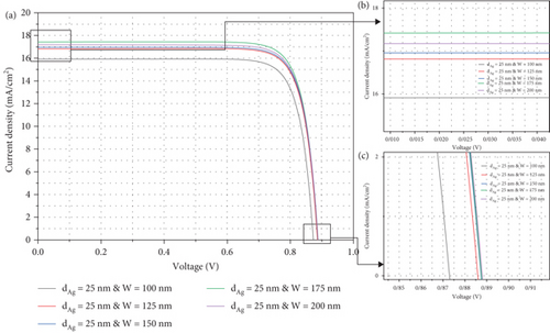
| PCE (%) | FF (%) | Voc (V) | Jsc (mA/cm2) | |
|---|---|---|---|---|
| W = 100 nm | 1.4212 | 0.8175 | 0.873 | 15.9061 |
| W = 125 nm | 12.2623 | 0.8381 | 0.886 | 16.4142 |
| W = 150 nm | 12.3487 | 0.815 | 0.887 | 16.96 |
| W = 175 nm | 12.6868 | 0.8206 | 0.8875 | 17.4186 |
| W = 200 nm | 12.4773 | 0.8182 | 0.8879 | 17.1721 |
2.2. Thermal Parameters
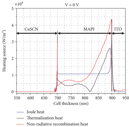
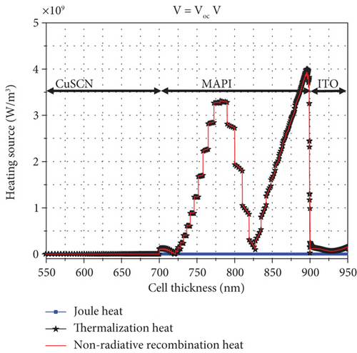
Figures 12(a) and 12(b) show the three-dimensional map of the total heat generated at two voltages V = Voc and V = 0 V, respectively, using Eq. (19). Like Figure 8, this figure also shows that the most heat generated at the boundary between the two layers of it is active and ITO.
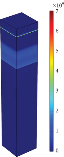
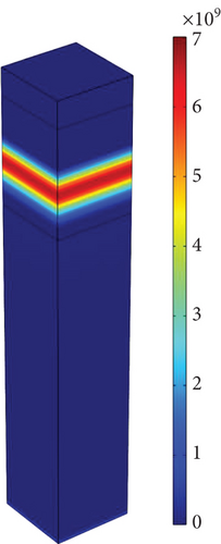
We also calculated Hsurf and HPeltier using Eqs. (13) and (15). Meanwhile, we neglected Hsurf at the boundary between the top and bottom layers, i.e., ITO/TIO2 and CuSCN/Au, because the recombination rate on the surface between these layers is insignificant. After all, near the bottom junction, which is made of Au, the hole-to-electron density ratio is higher, so the recombination rate is little.
Now, to compare the heat losses generated, the thermal power density in the system is shown in Figure 13, where Joule and thermal power density are the most effective in the system. In the Voc voltage, due to the decrease of the field and the natural decrease of the HJoule voltage, it gradually decreases.
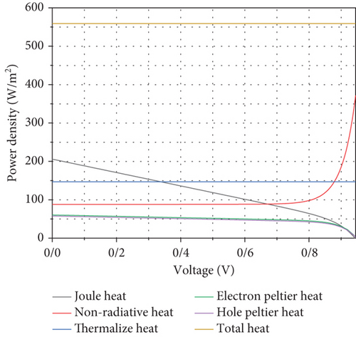
Also, at this voltage, the current density is equal to zero. That is why the HPeltier gradually decreases and reaches zero. Htotal is the total loss density in the system, and Pcell is the power density of the cell.
Now we examine how temperature behaves and its effect on current and voltage parameters. Figure 14 shows the current-voltage variation diagram for temperatures from 25 to 75°C. As we know, the temperature has a great effect on material properties (lifetime, bandgap, etc.), so temperature changes affect the cell performance and so the PCE. Therefore, we investigate the effect of temperature on the parameters and properties of solar cell materials. An increase in temperature causes an increase in the equilibrium population of the concentration of intrinsic carriers, which leads to an increase in the dark current density and, as a result, an increase in the recombination rate and a decrease in Voc. It also decreases slightly with an increase in the bandgap. An increase in temperature leads to a reduction in Voc and Jsc. It can reduce the amount of interest in the cell.
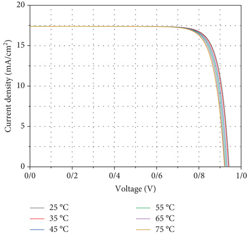
Table 9 displays changes in the values of Jsc, Voc, FF, and PCE for different temperatures in the cell. As mentioned, with the increase in temperature from the ambient temperature (25°C) to 75°C, the value of Voc has reduced a lot, and Jsc has decreased slightly, which causes a decrease in the PCE and the saturation coefficient in the cell.
| PCE (%) | FF (%) | Voc (V) | Jsc (mA/cm2) | |
|---|---|---|---|---|
| 25°C | 13.5394 | 0.8202 | 0.943 | 17.4 |
| 35°C | 13.4815 | 0.8195 | 0.94 | 17.3944 |
| 45°C | 13.378 | 0.8188 | 0.9336 | 17.3941 |
| 55°C | 13.2877 | 0.8180 | 0.9282 | 17.3937 |
| 65°C | 13.1972 | 0.8165 | 0.9237 | 17.3931 |
| 75°C | 13.1073 | 0.813 | 0.9213 | 17.3923 |
3. Conclusion
Here, we study the opto-electro-thermal (OET) characteristics, as well investigate carrier transport and thermodynamic behaviors inthe perovskite solar cell (PSC) structure. Aganoparticles (NPs) have been utilizedas plasmonic NPs in the structure of perovskite. This workexamines the thermal effects of NPs in the PSC structure. When the PSC is studied with two optical-electrical physics, the electrical parameters and the power conversion efficiency (PCE) are improved. Then, thermal physics has been applied in the simulation process, and the electrical parameters and the PCE were calculated. When Ag NP is not present in the structure, the values of Jsc, Voc, and PCE are 17.4 mA/cm2, 0.943 V, and 13.54%, respectively. When the NP was added to the system and its diameter increased, Jsc decreases from 17.33 to 10.33 mA/cm2, Voc reduces from 0.89 to 0.874 V, and the PCE in the system is decreased from 12.63 to 7.5%. The thermal investigation of the PSC with Ag NPs of different dimensions has shown that by increasing the diameter of NPs more than 50 nm, the presence of the NPs increases the thermal losses in the cell and creates destructive effects in the system. This causes that the construction of these cells in the real world is not recommended.
Conflicts of Interest
The authors declare no conflict of interest.
Authors’ Contributions
M.B did the simulations and wrote the draft and prepared the figures. D.F and M.E defined the project and prepared the final manuscript. D.F supervised the project and the presented results. D.F and M.E edited the manuscript. All authors reviewed the manuscript.
Open Research
Data Availability
The data that support the findings of this study are available from the corresponding author upon reasonable request.


