Improved Cu2ZnSnS4 Solar Cell Performance by Multimetallic Stacked Nanolayers
Abstract
This study utilized a postdeposition sulfurization method to produce thin films of the Cu2SnSnS4 (CZTS) absorber layer. Initially, metal precursors were deposited onto a tin oxide-coated substrate through thermal evaporation. Subsequently, sulfurization occurred in a mixed environment of sulfur vapor and argon gas. The sulfurization temperature was set at 500°C for a duration of 30 min. During the sulfurization process, the facile evaporation of tin compounds could lead to a deviation in the atomic ratio within the absorber layer and potentially result in the attachment of secondary phases to the surface of the absorber layer. Therefore, this study employed a multilayered metal precursor structure (with a constant total thickness for each metal and nonmetal sulfides as precursors) for sulfurization. This method effectively suppressed the formation of secondary phases, including ZnS within the absorber layer and SnS2 on the surface. From the quantification results, the ratio of ZnS to CZTS signal intensity decreased from 0.52 to 0, while the ratio of SnS2 to CZTS signal intensity dropped from 1.2 to 0. Additionally, the efficiency increased to 2.79%. In summary, this research introduced a novel preparation method to enhance the quality of CZTS films. The modification to a multilayered metal precursor structure reduced the evaporation of tin compounds, consequently minimizing the generation of secondary phases.
1. Introduction
Cu2ZnSn(S, Se)4 (CZTS(Se)) solar cells represent a promising category of thin-film photovoltaic technology; however, there exists a significant disparity between their highest efficiency and the theoretically maximum efficiency. This gap is attributed to the narrow phase stability range of CZTS(Se) materials, making them vulnerable to tin loss during high-temperature processing. This potential loss can lead to the creation of detrimental defects. These defects present a challenge in controlling the chemical stoichiometry and phase purity of the absorber layer, resulting in the formation of secondary phases, point defects, and deep recombination centers. The presence of these defects significantly reduces the open-circuit voltage (Voc), creating a bottleneck for the enhancement of CZTS(Se) solar cell efficiency [1, 2]. To address the issue of insufficient Voc, it becomes crucial to control the fundamental proportion and distribution of the absorber layer. Typically, fine grains appear at the bottom of the absorber layer due to inadequate reaction between ZnS(Se) and Cu–Sn–S(Se) phases. These fine grains lead to the formation of more grain boundaries and secondary phases, creating leakage pathways for photogenerated carriers towards the back contact, thereby, degrading the device performance. During the annealing process, the redistribution of metal elements in the precursor occurs, and the available copper migrates to the surface, forming the Cu2−xS(Se) phase, thereby, generating sulfur/selenium defects. Additionally, chemical stoichiometric deviations or condensation processes can lead to the formation of the secondary phase SnS(Se)2 on the surface of the absorber layer [3]. These secondary phases impede carrier collection by forming diodes, consequently reducing the Voc of the device. The highly asymmetric growth conditions result in compositional gradients, adversely affecting the film quality of the kesterite absorber layer [4]. Although the secondary phases Cu2−xS(Se) and SnS(Se)2 generated on the surface can be removed by chemical etching solutions to enhance device performance, for example, using KCN to remove Cu2−xS(Se) and (NH4)2S to remove SnS(Se)2 [5, 6]. However, these chemical etching solutions possess corrosive, toxic, and flammable characteristics, making them less than ideal for secondary phase removal methods [6]. Additionally, secondary phases generated within the absorber layer are not easily removable and may lead to the formation of film porosities. Therefore, the development of a simple and environmentally friendly secondary phase removal method becomes crucial. The stacking sequence of metallic precursors in CZTS(Se) has a significant impact on alloy formation, crystal growth, surface shape, and the distribution of secondary phases. Generally, in the stacking order of three metallic precursors (Sn/Cu/Zn), tin stacking is used as the bottom layer to improve thin film adhesion [7], with copper stacking in the middle layer due to its low volatility and high diffusion coefficient. Zinc stacking is positioned as the top layer to mitigate excessive Zn concentration at the bottom. However, according to the interdiffusion coefficient in Cu/Zn/Sn matrix [8], since the diffusion coefficients of tin in copper and zinc in copper are both low, this stacking order cannot provide uniform film growth. This may lead to the formation of secondary phases within the absorber layer, thereby reducing the performance of the device.
In addition to the aforementioned issues, the Mo back electrode substrate used in the standard process, besides forming MoS(Se)2 during high-temperature processes, may also generate an interface layer between the absorber layer and the back electrode (this interface layer consists of a disordered arrangement of phases), affecting the characteristics of the absorber layer and the overall device. Furthermore, the use of metal Mo as the back electrode prevents light from passing through, allowing only single-sided illumination, which limits its potential for combining with indoor light in the future. To address these challenges, many research teams have proposed using transparent conductive oxide (TCO) substrates as the back electrode. TCO substrates possess transparent and conductive properties, enabling light to pass through the back electrode, facilitating dual-sided illumination. Commonly used commercial TCOs include In2O3 (ITO) and SnO2:F (FTO). Although current research indicates that the precursor film can fully transform into CZTS at sulfurization temperatures of 500°C or higher, CZTS films prepared on ITO substrates at temperatures exceeding 500°C result in In diffusion from the ITO back contact into the CZTS absorber layer, reducing ITO conductivity and limiting efficiency improvements [9]. In comparison to ITO, FTO exhibits superior high-temperature stability. Research indicates that FTO/CZTS films, when annealed at temperatures below 580°C, still do not show the presence of an interface layer at the FTO/CZTS interface. This suggests that the chemical stability of FTO during high-temperature annealing is advantageous for serving as the back contact electrode for CZTS films [10]. The highest efficiencies reported for CZTS solar cells prepared on FTO and ITO substrates are as follows: In 2014, the team led by Ge et al. [11] achieved a solar cell efficiency of 3.4% by co-electrodepositing and sulfurizing CZTS films on ITO glass substrates. In 2017, the team led by Wang et al. [12] directly deposited CZTS films on FTO substrates using co-electrodeposition technology (without any additional interface layer), resulting in a device efficiency of 4.73% after sulfurization. However, these efficiencies are still much lower than those of CZTS solar cells using Mo as the back electrode, leaving significant room for improvement. In summary, this study adopted a multilayered metallic nanolayer precursor structure on FTO substrates to control element distribution, thereby, reducing diffusion distances and controlling the formation of secondary phases. This offers a simple, convenient, and environmentally friendly approach to enhance the quality of the absorber layer film.
2. Experiments
This study employed a vapor deposition followed by a sulfurization process to prepare CZTS thin films. Initially, at room temperature, Sn/Cu/Zn metallic precursors were sequentially deposited on a commercially available FTO glass substrate using vapor deposition, defined as one layer of stacking. During the deposition of metal precursors, the chamber is first evacuated until reaching a vacuum level of 5 × 10⁻⁶ torr, after which deposition begins. The substrate remains unheated throughout the deposition process, and a 3-min pre-evaporation step precedes the deposition of each metal precursor. The deposition rate for all metals is maintained at 0.2 nm/s. Following pre-evaporation, the shutter is opened to deposit a single metal precursor until reaching the desired thickness, after which the shutter is closed. This sequence is repeated for each subsequent metal, cycling through the process. Ultimately, the total thicknesses are approximately 267 nm for Sn, 153.6 nm for Cu, and 142.8 nm for Zn. By employing a divided approach for the Sn/Cu/Zn precursors, films with two layers, three layers, and four layers were individually fabricated (with the total thickness of each metal kept constant, as illustrated in Figure 1). Subsequently, the deposited four sets of precursors were placed in a quartz box (the quartz box used in this study exhibits good airtightness). Simultaneously, 6000 mg of sulfur powder was added to the quartz tube for sulfurization. The maximum sulfurization temperature was set at 500°C. Throughout the process, Ar gas was continuously introduced, and the gases involved in the reaction were filtered and carried out through the evacuation device of the dry adsorption tower. The sulfurized samples are defined according to the number of precursor layers as follows: one layer—3L, two layers—6L, three layers—9L, and four layers—12L. The prepared samples underwent measurement and analysis of film microstructure, morphology, and optical properties using X-ray diffraction (XRD), field emission scanning electron microscopy (FE-SEM; JXA-8530F Pus, JEOL), energy dispersive spectroscopy (EDS), Raman scattering, UV-vis-NIR Spectrophotometer (V670, JASCO), Raman spectroscopy, and secondary ion mass spectrometry (SIMS). XRD analysis was performed using a SIEMENS D500 X-ray diffractometer with Cu Kα radiation (wavelength of 1.5418 Å). During the scan, the diffracted beam rotated by 0.005°, scanning the angular θ−2θ range from 10° to 80°, with an integration time of 1 s for each data point. Raman microspectroscopy measurements were carried out at room temperature using an Ar laser (514.5 nm) and a He–Cd laser (325 nm), along with a Horiba Triax (Jobin Yvon) triple monochromator and a TE-cooled charge coupled device (CCD) detector. After fabricating the CZTS absorber layer, a chemical bath deposition (CBD) method was employed to prepare an approximately 50 nm CdS layer, sputtering was used to deposit about 50 nm of i-ZnO, and approximately 300 nm of ZnO:Al (AZO). Subsequently, sputtering was again employed to deposit approximately 50 nm of Ni and approximately 1 μm of Al as the top electrode (effective area of the CZTS device is 0.18 cm2). Following the fabrication of the CZTS solar cell, current density–voltage (J–V), curve was measured to determine the photovoltaic characteristics of the device. The measurement with incident light was performed in an environment with a solar simulator (Newport 94022A) that generated an air mass (AM) 1.5 global standard spectrum with a light intensity of 1000 W m−2 (i.e., 1 sun). External quantum efficiency (EQE), and electrochemical impedance spectroscopy (EIS) measurements were conducted to characterize the optoelectronic properties of the devices, with the environmental temperature controlled at 25 ± 1°C during the measurements. The specimens’ EQE spectra were acquired using a 300 W xenon lamp (Newport 66984) as the light source and a monochromator (Newport 74112). The spot size projected onto the specimen was approximately 1 mm × 3 mm.

3. Results and Discussions
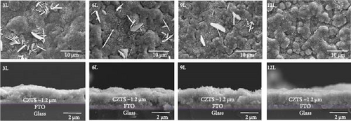
Figure 2 presents the SEM top-view and cross-sectional images of samples 3L, 6L, 9L, and 12L. The thickness of all CZTS films is approximately 1.2 μm. Especially noticeable are sheet-like structures observed on the surfaces of samples 3L, 6L, and 9L. Regarding these sheet-like structures, we conducted EDS measurements (not shown here), revealing the presence of SnSx compounds, consistent with the literature [6, 13, 14]. The existence of SnS2 on the surface of CZTS films can significantly impact the devices by forming diodes and hindering carrier collection, consequently reducing the Voc of the devices [6]. Furthermore, with an increase in the number of precursor stacking layers, there is a gradual decrease in SnSx. By the time we reach sample 12L, there are no apparent sheet-like structures on the sample surface.
Subsequently, we used EDS to measure the atomic percentages of Sn, Cu, Zn, and S in samples 3L, 6L, 9L, and 12L, with the results shown in Figure 3. As the number of precursor stacking layers increases, the Sn content rises, while the Zn content slightly decreases. This is attributed to the increased interface area between Cu and Sn due to the higher number of precursor stacking layers, resulting in a greater distribution of Cu–Sn alloys that can effectively suppress the loss of Sn atoms during the sulfurization process at high temperatures. The slight decrease in Zn atoms may be attributed to the influence of metal diffusion. According to the metal diffusion table, the diffusion capability between Cu and Zn is relatively poor. Therefore, in the precursor of sample 3L, the uppermost layer of Zn tends to react with S, forming more ZnS. As the number of precursor layers increases, the contact area between Zn and Sn increases. The diffusion capability between Zn and Sn, which are adjacent, is stronger than that between Cu and Zn, contributing to a more uniform distribution. Additionally, the melting point of Zn-related alloys is lower than that of ZnS. Consequently, with an increasing number of precursor layers, there is a slight decrease in Zn atoms. During the sulfurization process of CZTS, SnSx tends to re-evaporate from the sample. However, due to the better airtightness of the quartz box used in this study and the natural cooling process, SnSx is less likely to escape, leading to its accumulation inside the quartz box. These SnSx compounds are unlikely to react again with Zn-related compounds on the surface of the sample to form new compounds; instead, they tend to adhere to the surface as SnSx compounds [15]. Therefore, during the high-temperature sulfurization process, as the number of precursor layers increases, the amount of SnSx re-evaporation may decrease, resulting in less SnSx adhering to the surface of the sample.
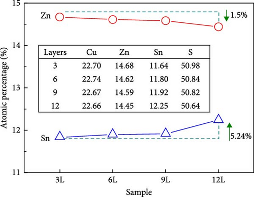
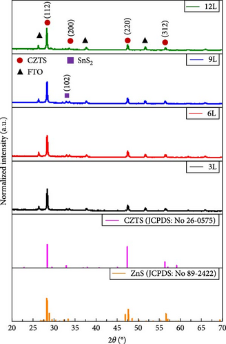
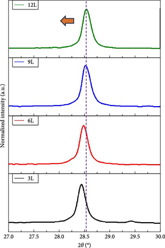
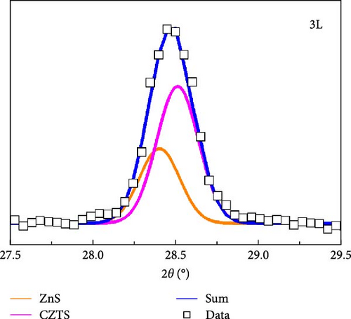
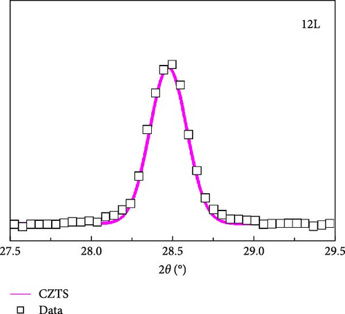
Figure 4a presents the XRD measurements of samples 3L, 6L, 9L, and 12L after normalization. All samples exhibit diffraction peaks corresponding to CZTS at (112), (200), (220), and (312), along with the diffraction peaks of the FTO substrate. In samples 3L, 6L, and 9L, diffraction peaks of the secondary phase SnS2 at (102) are observed, consistent with the SEM results. Subsequently, the (112) diffraction peak is magnified, as shown in Figure 4b. It can be observed that with a decrease in the number of precursor layers, the (112) diffraction peak gradually shifts towards lower angles. The shift may be attributed to the difference in ionic radii between Zn and Sn elements, leading to increased stress, or it could be influenced by other secondary phases. To further investigate, Gaussian fitting was applied to the (112) diffraction peaks of samples 3L and 12L, as illustrated in Figure 4c. The results reveal diffraction peaks corresponding to CZTS (joint committee on powder diffraction standards [JCPDS]: 26-0575) and ZnS (JCPDS: 89-2422) in sample 3 L [16, 17]. We quantified the amount by dividing the peak intensity of ZnS by that of CZTS, with the results showing a ratio of 0.52 for sample 3L and 0 for sample 12L. This indicates a gradual reduction in the amount of ZnS within the absorber layer; however, due to the very close proximity of the characteristic peaks of CZTS and ZnS in the XRD analysis, further confirmation of the presence of ZnS will be conducted in subsequent analyses. In addition, the lattice constants of samples 3L, 6L, 9L, and 12L were calculated. According to the literature, the ideal CZTS bulk material has lattice constants a and c of 5.43 Å and 10.86 Å, respectively [18]. The corresponding values for samples 3L, 6L, 9L, and 12L are as follows: sample 3L (a = 5.42 Å, c = 10.8 Å), sample 6L (a = 5.43 Å, c = 10.83 Å), sample 9L (a = 5.43 Å, c = 10.85 Å), and sample 12L (a = 5.43 Å, c = 10.86 Å). With an increase in the number of layers, the lattice constants of CZTS show a tendency to increase. This could be attributed to the reduction in the loss of Zn and Sn, filling defects, and resulting in an increase in lattice constants. The structure of sample 12L is closest to that of CZTS bulk material, indicating an improvement in crystal quality.
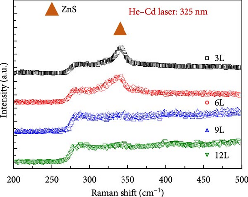
To further confirm the presence of secondary phases in the samples, we conducted Raman spectroscopy measurements to distinguish CZTS from secondary phases. For accurate detection of secondary phases in the CZTS absorption layer, the resonance condition of Raman spectroscopy had to be employed [19]. Two different light sources were utilized: an Ar laser (wavelength: 514.5 nm) and a 325 nm He–Cd laser (wavelength: 325 nm) were employed to probe the secondary phases in the CZTS absorption layer. Figure 5a shows the Raman spectra obtained using the 514.5 nm laser, revealing characteristic peaks for CZTS at approximately 287, 333, and 365 cm−1 in all samples under A1 mode. Additionally, a signal corresponding to SnS2 secondary phase was observed around 310 cm−1, with the signal decreasing gradually with an increase in the number of precursor layers. To further quantify the ratio of SnS2 to CZTS within the absorber layer, we first define the intensity of the 310 cm−1 signal as I1 and the intensity of the 333 cm−1 signal as I2. The ratio I2/I1 represents the proportion of SnS2 in the CZTS thin film. The calculated I2/I1 values are 1.2 for 3L, 0.9 for 6L, 0.43 for 9L, and 0 for 12L. This indicates that as the number of precursor layers increases, the variation in the proportion of SnS2 on the surface of the CZTS thin film aligns with the previously observed results. Figure 5b displays the Raman spectra obtained using the 325 nm laser, indicating a peak at approximately 343.6 cm−1 for ZnS in samples 3L and 6L, consistent with the literature [19]. The signal for sample 6L is less pronounced compared to sample 3L, and there is no significant ZnS peak observed in samples 9L and 12L. However, according to the EDS measurement results, the Zn/Sn ratios for samples 3L, 6L, 9L, and 12L were 1.26, 1.24, 1.22, and 1.18, respectively. Despite this, ZnS signals were not detected in sample 9L, possibly due to the skin depth. The skin depth is influenced by the conductivity of the thin film and the frequency of the incident photons. Therefore, as the energy of the incident photons increases (wavelength decreases), the penetration depth decreases [20]. Since the wavelength of the He–Cd laser (325 nm) is shorter than that of the Ar laser (514.5 nm), the penetration depth measured by the Ar laser is greater than that measured by the He–Cd laser on the same specimen.
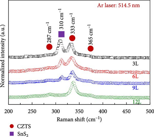
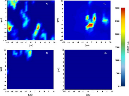
Additionally, the shoulder peak at around 287.5 cm−1 showed minimal changes. According to the literature, this peak is associated with CZTS, and therefore, the changes are not significant [21]. To gain a better understanding of the distribution of the SnS2 secondary phase on the surface of the absorber layer, Raman mapping was performed on each sample surface (with a laser wavelength of 514.5 nm). Figure 5c illustrates the Raman mapping results for samples 3L, 6L, 9L, and 12L, defining the region in the A1 mode with a frequency range of 310–313 cm−1 as the SnS2 secondary phase. The measured area was 20 μm × 20 μm. As the number of precursor layers increased, the distribution of SnS2 on the surfaces of samples 3L, 6L, 9L, and 12L gradually decreased, and SnS2 was not observed in sample 12L. The analysis from the Raman mapping confirms that with an increasing number of precursor layers, the SnS2 secondary phase on the sample surface gradually diminishes, consistent with the previous XRD and SEM results.
To facilitate a better understanding of the distribution of elements within the CZTS film, Figure 6a illustrates the SIMS measurement results for samples 3L, 6L, 9L, and 12L. Each figure is divided into two parts, representing CZTS and FTO, respectively. In the absorptive layer of the 3L sample, the distribution of elements appears uneven, but with an increase in the number of precursor layers, the distribution of elements within the CZTS film gradually becomes more uniform. Figure 6b compiles the Zn depth profiles for samples 3L, 6L, 9L, and 12L. It can be observed that, although the Zn component in the CZTS film becomes more uniform, sample 9L still exhibits a higher Zn concentration in the region of approximately 250–750 nm. However, no signal of ZnS was detected in the Raman measurements. This may be attributed to the use of a 325 nm laser, with a measurement depth of approximately 50 nm [22], preventing the detection of deeper secondary phases and resulting in the absence of the ZnS phase in sample 9L.
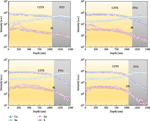
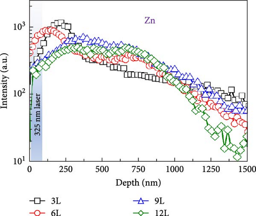
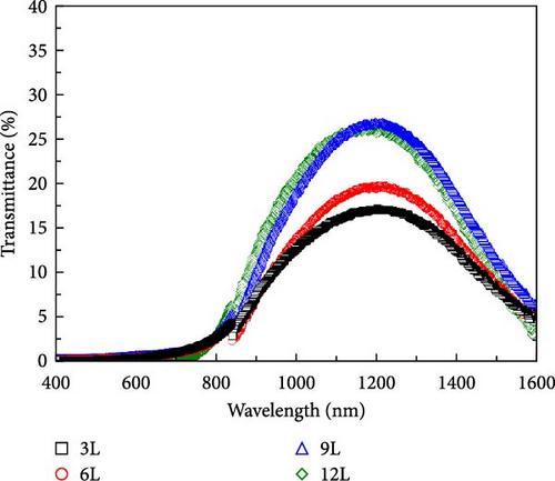
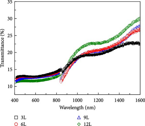
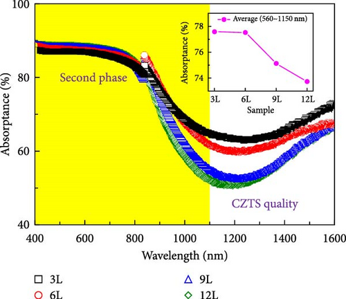
Figure 7a–c, respectively, present the UV–vis–NIR spectroscopy results of the transmittance, reflectance, and absorbance for samples 3L–12L deposited on FTO substrates. From the inset in Figure 7c, it can be observed that with an increase in the number of precursor layers, the absorbance in the visible light range (400–800 nm) decreases. This variation may be influenced by the quantity of secondary phases. The known secondary phases in this study include SnSx and ZnS compounds. However, due to the bandgap of ZnS-related compounds being approximately 3.6 eV, primarily absorbing in the ultraviolet region, and SnSx-related compounds having a bandgap of about 1.07–2.2 eV, mainly absorbing in the visible light region, the changes in absorbance in the visible light region are likely primarily influenced by the quantity of SnSx. Furthermore, the changes in absorbance in the infrared region increase with an increase in the number of precursor layers, possibly related to the quality of the CZTS film. Figure 7d illustrates the absorption coefficients calculated using the following formula [23]:
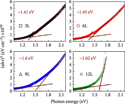

α is the absorption coefficient, h is the Planck constant, ν is the photon frequency, and A is a constant. In the plot of (αhν)2 against photon energy (hν), the energy gap can be calculated by extrapolating (αhν)2 linearly and taking the intercept on the hν axis [24]. To further understand the reasons for the variation in the energy gap, the number of precursor layers, energy gap, and the ratio of Cu/(Zn + Sn) are plotted in Figure 7e. It can be observed that as the number of precursor layers increases, the Cu/(Zn + Sn) ratio gradually decreases, and the energy gap increases. This may be attributed to the hybridization of Cu’s d orbitals with S’s p orbitals, consistent with literature findings [25].
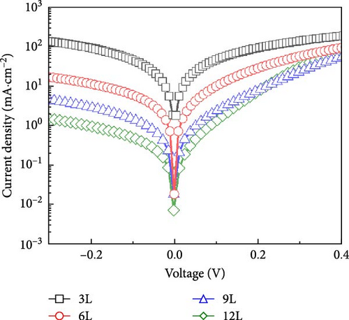
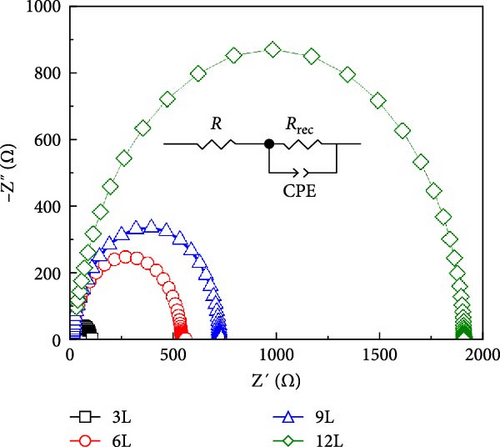
Figure 8a,b depict devices fabricated from thin films of samples 3L−12L, with measurements of J–V and EIS conducted in a dark environment. The characteristics of the devices are listed in Table 1. Figure 8a illustrates the diode characteristics of the devices in the dark. It is evident from Table 1 that, in the dark environment, the J–V plot can be distinguished into two distinct regions. The measurement range of Region I is −0.3 to 0.3 V, where the current density characteristics are primarily influenced by shunt leakage current and space charge limitations. Above 0.3 V is Region II, representing diode current. In Region I, it can be observed that the leakage current decreases with an increase in the number of precursor stacking layers, leading to an improvement in leakage current. The main reason for this improvement is influenced by the quantity of SnS2 on the CZTS surface. Due to the relatively thicker single-metal layer in sample 3L, the elements are less prone to diffusion, resulting in an uneven distribution of elements within the thin film. However, in the case of modified metal precursor stacking with adjusted layer thickness and structure, it facilitates diffusion between metal layers, promoting a gradual homogenization of elements within the film. The increased distribution of Cu6Sn5 alloy contributes to the reduction of Sn loss, subsequently lowering the quantity of SnS2 on the surface of the CZTS thin film. Simultaneously, as the elements within the thin film become more uniform, the secondary phase ZnS gradually diminishes. The rectifying characteristics of the device can be represented by the ratio of current values at 0.3 to −0.3V in the J–V curve measured in a dark environment (i.e., Idark [0.3 V]/Idark [−0.3 V]) [26]. A higher rectifying ratio signifies better rectifying characteristics of the device. Table 1 outlines the rectifying characteristics of devices from samples 3L−12L. It can be observed from the rectifying characteristics that, with an increase in the number of precursor stacking layers, the rectifying characteristics gradually improve. In the case of sample 12L, the rectifying characteristics reach their optimal state.
| Sample | AM 1.5G | Dark | |||||||
|---|---|---|---|---|---|---|---|---|---|
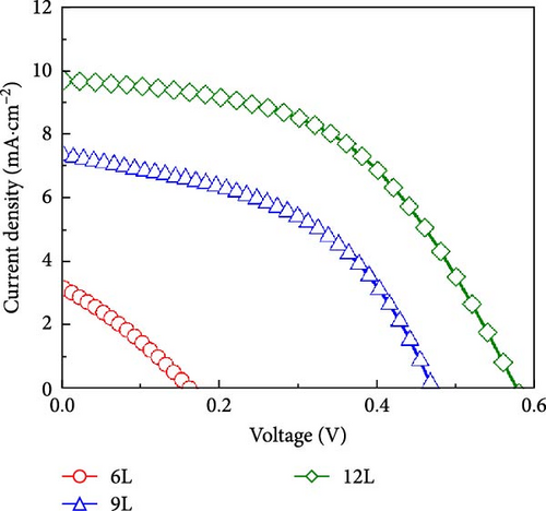
| Voc (V) | Jsc (mA/cm2) | FF (%) | Eff. (%) | Rectifying characteristics | CPE-T (F·cm−2) | CPE-P (F·cm−2) | R (Ω·cm2) | Rrec (Ω·cm2) | |
| 3L | N.A. | N.A. | N.A. | N.A. | 1 | 0 | 1 | 25.6 | 75.1 |
| 6L | 0.17 | 3.17 | 28 | 0.15 | 3.37 | 7.63E-08 | 0.96 | 13.57 | 526.5 |
| 9L | 0.47 | 7.37 | 47 | 1.63 | 5.04 | 5.78E-08 | 0.97 | 20.22 | 702 |
| 12L | 0.56 | 9.74 | 51 | 2.79 | 19.89 | 4.00E-08 | 0.94 | 17.01 | 1891 |
- Abbreviations: 3L, one layer; 6L, two layers; 9L, three layers; 12L, four layers; AM, air mass; CPE, constant phase element; CPE-P, constant phase element-ideal capacitance; CPE-T, constant phase element-interface capacitance; CZTS, Cu2SnSnS4; Eff, power conversion efficiency; FF, fill factor; Jsc, short-circuit current; R, resistor; Rrec, composite resistor; Voc, open-circuit voltage.
Figure 8b illustrates the Nyquist plot obtained through EIS in a dark environment. The schematic in Figure 8b outlines the equivalent circuit model used in this analysis, indicating the nonuniform chemical composition and shape around the CdS/CZTS interface. The circuit model consists of a resistor (R), a constant phase element (CPE), and a composite resistor (Rrec). The EIS measurement results were fitted using this circuit model. The fitting results of the Nyquist curve are presented in Table 1. From the table, it can be observed that R is associated with contact and material resistance, such as FTO contact, and AZO front window, and Al contact grid. CPE is defined as CPE-T and CPE-P, respectively, related to interface capacitance and ideal capacitance. The parallel capacitors and resistors corresponding to low-frequency and high-frequency sides of the Nyquist plot describe the alternating current (AC) response in the CZTS/CdS heterogeneous interface. Since the contact electrodes used in this study are made from the same material and have identical parameters, noticeable differences in resistance values (R) are not observed. However, Rrec represents the composite resistance, which is inversely proportional to the charge recombination rate of the device. As the number of precursor stacking layers increases, the Rrec value around the CZTS/CdS interface in CZTS solar cells gradually increases. Since the CdS layer used in this study was prepared under the same conditions and with identical parameters, the influence of Rrec is mainly attributed to the surface SnS2 and secondary phase ZnS in the CZTS absorption layer. According to literature results, in the CZTS layer, if a leakage current path is generated in the CZTS cell, the Rrec value in the CZTS solar cell will be lower than the expected leakage current path value [27], consistent with the results in Figure 8a.
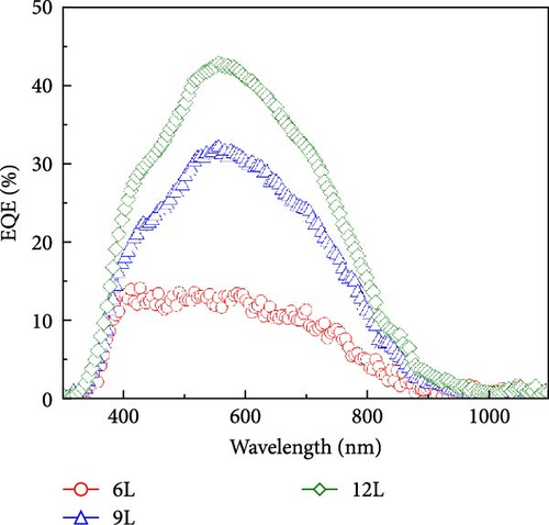
Figure 8c illustrates the J–V curves measured under AM 1.5G illumination for devices fabricated from thin films of samples 3L−12L, with the characteristics of the devices also listed in Table 1. Under AM 1.5G illumination, as the number of precursor stacking layers increases, the photovoltaic conversion efficiency, Voc, short-circuit current, and fill factor gradually improve. This improvement is mainly attributed to the reduction of CZTS surface SnS2 and secondary phase ZnS, thereby enhancing the diode characteristics. The measurement of EQE contributes to understanding the mechanism of carrier losses in CZTS devices. Figure 8d illustrates the EQE response of solar cells fabricated from 6L−12L thin films. Noticeable EQE losses are observed below approximately 510 nm, primarily due to material absorption in the CdS and ZnO layers. In the wavelength range beyond 510 nm, EQE losses are mainly influenced by the content of SnSx and secondary phases like ZnS. Elevated levels of secondary phases increase defect density, thereby, raising the recombination rate of charge carriers in the solar cell. With an increase in the number of precursor stacking layers, EQE losses significantly decrease, consistent with the improvement in device rectification characteristics. Consequently, from the analyses of J–V, EQE, and EIS, it is concluded that the presence of lamellar SnSx and ZnS secondary phases on the CZTS surface diminishes the conversion efficiency of CZTS solar cells, and an increased number of precursor stacking layers effectively reduces the formation of SnSx and ZnS secondary phases.
4. Conclusion
The research findings indicate that with an increase in the number of precursor stacking layers deposited on the FTO substrate, there is an effective suppression of secondary phases such as SnS2 and ZnS in the CZTS film. The ratio of ZnS to CZTS signal intensity decreased from the initial 0.52 to 0, while the ratio of SnS2 to CZTS signal intensity dropped from the initial 1.2 to 0. Simultaneously, it improves the uniform distribution of elements and the size distribution of grains within the film. This may be attributed to the increased distribution of Cu6Sn5 alloy with the growing number of precursor stacking layers. Consequently, during the sulfidation process, it effectively suppresses the loss of Sn atoms, reducing the deviation in atomic proportions within the absorption layer and promoting the growth of CZTS grains. These improvements help enhance the photovoltaic performance of the solar cells, particularly in reducing leakage current. This has increased the efficiency of the devices from previously ineffective to 2.79%. Furthermore, EIS measurements have been used to further analyze and quantify the impact of secondary phases on device performance, which aids in improving the manufacturing process and performance of the devices. These results suggest that optimizing the stacking sequence of metal precursors plays a crucial role in enhancing overall performance, particularly in the context of applications such as solar cells.
Conflicts of Interest
The authors declare no conflicts of interest.
Author Contributions
Conceptualization: F.-IL. and S.-Y.K. Methodology and investigation: J.-F.Y. and K.-J.L. Validation: F.-IL., S.-Y.K., and J.-F.Y. Formal analysis: K.-J.L. Resources: F.-IL. and S.-Y.K. Data curation and writing–original draft preparation: J.-F.Y. Writing–review and editing and supervision: S.-Y.K. Project administration: F.-IL. Funding acquisition: F.-IL., S.-Y.K., and K.-J.L. All authors have read and agreed to the published version of the manuscript.
Funding
This research was supported by Chang Gung Memorial Hospital (Grant BMRP 956) and National Science and Technology Council (Grants NSTC 113-2221-E-155-037, 113-2221-E-182-056-MY3, and 113-2622-E-182-003).
Acknowledgments
This research was supported by Chang Gung Memorial Hospital (Grant BMRP 956) and National Science and Technology Council (Grants NSTC 113-2221-E-155-037, 113-2221-E-182-056-MY3, and 113-2622-E-182-003).
Open Research
Data Availability Statement
The data supporting the findings of this study are available within the article.


