[Retracted] Design of Image Acquisition System Based on Visual Intelligent Sensor and Video Signal Processing
Abstract
With the rapid development and iteration of CMOS image sensor and other related technologies, in addition to the more advanced technology, the corresponding sensor also integrates the image signal processing system, so it is a leap for the image acquisition system. Based on this, this paper will take the visual intelligent sensor produced and developed by a semiconductor company as the hardware to complete the hardware design of the image acquisition and transmission system. In addition to the core processor of the system, this paper will also use audio and video processing chips and image data processing chips for collaborative analysis, so as to ensure the processing capacity and processing quality of the image acquisition system at the hardware design level. Compared with the traditional system, at the corresponding system software level, in order to further improve the quality of video signal processing, this paper creatively proposes a switch weighted median filter denoising algorithm, which has a significant impact on the processing of random impulse noise in video and the overall image filtering. At the same time, the algorithm also protects the edge details of the video image, thus improving the authenticity of the image and video. Based on this, this paper has built a verification platform based on supporting hardware and corresponding algorithms. Through hardware debugging and system operation analysis, when the operating frequency of the visual intelligent sensor is 100 MHz, the set acquisition depth is 10 bits, and the corresponding system collects data at a rate of 251 fps per second. In terms of the corresponding performance, the iteration number of the algorithm proposed in this paper is about 40% more than that of the traditional algorithm in unit time. In terms of the corresponding algorithm performance, the algorithm proposed in this paper is about 30% higher than the traditional algorithm. In terms of the efficiency of the corresponding image and video acquisition system, the algorithm proposed in this paper is about 44% higher than the traditional algorithm. Based on this, the system proposed in this paper has obvious advantages over the traditional algorithm.
1. Introduction
The core of visual intelligent sensor is mainly the hardware equipment based on CMOS image sensor, which has the advantages of low power consumption, high processing performance and small size. With the rapid iterative development of semiconductor technology and related integration technology, modern visual intelligent sensors also has a large number of integrated digital signal processors, which makes the sensors have the function of digital signal processing. Therefore, the corresponding performance of visual intelligent sensors with CMOS image sensors as the core technology is also becoming stronger [1–3]. Compared with the traditional CCD image sensor, the visual intelligent sensor with CMOS image sensor as the core technology has gradually replaced the CCD image sensor with the continuous progress of technology and the continuous iteration of the corresponding image processing algorithm and has gradually become the mainstream sensor in the field of video image processing [4, 5]. When designing the image and video detection system based on CMOS image sensor, there are uncertainties in the collection and processing of video image data. Therefore, compared with the design of traditional CCD sensor, it needs to pay more attention to the cooperative use of a variety of signal processing chips, so that the finally designed image and video processing system has certain processing flexibility and convenience [6–8]. Based on the above analysis, the image processing hardware system design of visual intelligent sensor based on CMOS image sensor needs to fully consider various factors to give full play to the performance advantages of the sensor, so as to provide hardware guarantee for image and video data transmission and improve the correctness of data processing analysis [9, 10].
The traditional mainstream video image information acquisition and processing technology mainly includes image data processing technology based on MCU, image data processing technology based on DSP, image data processing technology based on FPGA, and image data processing technology based on MCU. The above image data processing technology is mainly due to the different design of its corresponding data acquisition system due to the different corresponding hardware core devices [11, 12]. In addition to hardware, traditional video image signal processing algorithms rely more on the powerful performance of hardware technology to ensure the restoration degree of image and video, so as to ensure the processing quality of image and video. The corresponding data processing speed also depends heavily on the processing speed of hardware. At the same time, in the corresponding random noise anti-interference level, traditional image data processing algorithms also rely on the filtering ability of hardware equipment, and the corresponding processing algorithm does not have filtering capability [13–15]. However, with the increasingly complex use environment corresponding to the image and video processing system, a large number of random impulse noise will inevitably be encountered in the process of image and video acquisition, transmission, and processing, which will seriously affect the quality of image and video. This has created a huge processing pressure on the image signal processing algorithm, and it is also very difficult for the later basic processing such as image mosaic and scaling [16]. The traditional data processing algorithms have carried out technical iteration at the filtering level. The corresponding filtering algorithms such as median filtering, weighted filtering, switching filtering, and PWMAD filtering algorithms have also solved the problem of filtering random impulse noise in image and video to a certain extent. However, these filtering algorithms have lost the edge details of the image to varying degrees, and the corresponding image quality has been greatly reduced. Based on this, in addition to the design of the hardware system, the research on the image data signal processing algorithm is also very urgent, which plays an important role in improving the performance of the image acquisition system [17].
Based on the above analysis, it takes the visual intelligent sensor with CMOS image sensor as the core technology as the hardware technology and optimizes its image data processing algorithm. The main research contents are as follows: This paper mainly completes the hardware design of the image acquisition and transmission system based on the visual intelligent sensor developed by a semiconductor company. In addition to the core processor of the system, this paper will also use audio and video processing chips and image data processing chips for collaborative analysis, so as to ensure the processing capacity and processing quality of the image acquisition system at the hardware design level. At the corresponding software level, in order to further improve the quality of video signal processing, a weighted median filter denoising algorithm is proposed, which has significant advantages in the processing of random impulse noise in video and the overall image filtering. At the same time, it also well protect the edge details of video image, so as to improve the authenticity of image and video. Based on this, this paper has built a verification platform based on supporting hardware and corresponding algorithms. Through hardware debugging and system operation analysis, when the operating frequency of the visual intelligent sensor is 100 MHz, the set acquisition depth is 10 bits, and the corresponding system collects data at a rate of 251 fps per second. In this case, the image acquisition system works stably. The corresponding restoration degree of the video image is higher, and the image transmission quality is higher.
Based on the above analysis, the structure of this paper is arranged as follows: the second section of this paper mainly analyzes the research status of the design of image acquisition system for visual intelligent sensor and its video signal processing; The third section of the article mainly discusses the design of image acquisition system based on visual intelligent sensor and its video signal processing, analyzes and studies the mechanism of on-off weighted median filter denoising algorithm in detail, builds a set of image and video acquisition system based on visual intelligent sensor, and gives the corresponding design details. The fourth section of the article will verify and analyze the operation results of the system in the above environment by debugging the hardware and analyzing the operation of the system. Under the condition that the working frequency of the visual intelligent sensor is 100 MHz, the set acquisition depth is 10 bits, and the corresponding system collects data at a rate of 251 fps per second. Finally, it will be summarized.
2. Related Research: Analysis of Research Status of Image Acquisition System Design
In order to improve the performance of the image and video acquisition, transmission, and analysis system, some researchers have conducted research and analysis on it. The main research focuses on two levels: the research on the hardware sensor level and the research on the software processing algorithm level. In terms of hardware sensors, relevant researchers of the Korean Academy of Sciences [18] have proposed a hardware sensor combination based on dsp+fpga. In the whole sensor system, the corresponding DSP and FPGA operate, respectively. FPGA is mainly responsible for the integration, storage, and interface of image and video data, while the corresponding DSP is mainly responsible for data processing and analysis. This hardware sensor scheme improves the data processing performance of hardware to a certain extent, improve the processing speed and efficiency, and also improve the data throughput. Relevant scholars in Chinese Mainland [19, 20] have proposed and designed a set of CMOS sensor image information acquisition system, and its corresponding hardware core is also a combination of dsp+fpga. In such a system, the corresponding FPGA mainly preprocesses and compresses CMOS data and then sends it to DSP for format conversion output. The system improves the processing and analysis performance of the hardware system in the face of high-resolution images, and it further improves the image storage capacity of the system. At the level of video image data acquisition and analysis algorithms, the main research focuses on the removal of video image noise. The relevant Japanese Research Institute [] has proposed a median filtering algorithm for random impulse noise, which is mainly a nonlinear filter based on statistical ranking. The experimental results [21, 22] show that the algorithm can effectively suppress the corresponding impulse noise. However, this algorithm also highlights its shortcomings, that is, it cannot protect the edge details of the image, and the corresponding image quality is damaged. In order to protect the edge details of image and video, relevant scholars [23, 24] put forward a weighted filtering algorithm, which mainly processes the corresponding images with different degrees of smoothness according to different pixel weight coefficients. The experimental results of the algorithm show that it has the ability to protect the corresponding image and video details, but it has certain defects in the image and video processing speed and efficiency. Relevant research institutions [25, 26] in the United States have proposed a switching filtering algorithm for the above problems, which classifies the corresponding impulse noise into noise pixels and normal pixels and processes the weighting function based on this. To a certain extent, this method has the advantages of protecting image edge details and improving processing efficiency. Based on the above analysis, it is of great significance and practical value to design an image acquisition and analysis system that can not only have high-efficiency processing performance but also ensure the image and video edge details.
3. Design and Analysis of Image Acquisition System Based on Visual Intelligent Sensor and Video Signal Processing
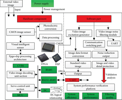
This section mainly discusses the design of image acquisition system based on visual intelligent sensor and its video signal processing, analyzes and studies the mechanism of on-off weighted median filter denoising algorithm in detail, builds a set of image and video acquisition system based on visual intelligent sensor, and gives the corresponding design details. Based on this, the corresponding overall system architecture is shown in Figure 1, the image and video acquisition system. It is mainly based on the visual intelligent sensor with CMOS image sensor as the core, and the corresponding image processing chip is carried out in the form of fpga+dsp. The hardware part mainly includes the video image decoding unit part and the corresponding servo control unit part. The corresponding CMOS image sensor mainly converts the photo electricity corresponding to the image or video to generate the corresponding processing data. At the same time, the corresponding data is amplified and converted into digital signals through the internal digital to analog conversion chip. Finally, the corresponding digital signals are transmitted to the external interface in the corresponding format. Based on this, the CMOS image sensor selected in this paper is a single core visual image processing sensor of a semiconductor company. Its corresponding integrated image processing system has the advantages of low cost and high performance. The corresponding software part mainly includes the video image excitation generator part, the video image noise filtering module part, and the communication exchange part. The corresponding video image excitation generator part is mainly responsible for the corresponding system conversion of the video images, and the corresponding standard video images are output one by one according to the time sequence, and finally, the output data is sent to the FPGA part for digital processing and analysis. In the corresponding video image noise filtering module, the image data output from the hardware video image acquisition system is mainly filtered and denoised, and the details of the image and video are protected. The noise mainly removed includes random impulse noise. The corresponding communication exchange part is mainly based on UART module for information exchange and analysis, so as to realize the efficient operation of the entire image and video acquisition system.
3.1. Research on the Mechanism of On-Off Weighted Median Filter Denoising Algorithm
In order to further optimize the image and video filtering quality of the video image acquisition system, this paper improves the image and video filtering algorithm, while preserving the corresponding edge details as much as possible.
Based on the above problems, this paper proposes an on-off weighted median filter algorithm. The corresponding algorithm flow is shown in Figure 2 below. Its main core idea is to replace the domain pixels of the monitored points with normal pixels that are approximately normal. At the same time, set the value with large gray difference between pixels in the normal environment as the critical point for judging noise pixels. At this time, determine whether the pixels are noise pixels through this critical point.
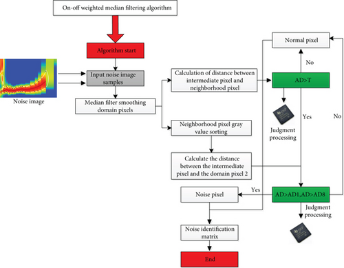
As can be seen from the above flow chart, the execution details of the corresponding algorithm are as follows:
Step 1: carry out the corresponding median filtering for the pixels around each pixel point to be detected in the image, select the center coordinates of the corresponding detected pixel point, and filter the 8 pixels around it. At this time, the gray value probability corresponding to the corresponding adjacent pixel points will be replaced by the gray value of the normal pixel.
Step 2: smooth the corresponding domain pixels, calculate the distance between the intermediate pixels and the domain pixels, and reasonably sort the gray values of the domain pixels.
Step 3: when the corresponding distance value is greater than the corresponding threshold value, a second judgment is made. The corresponding judgment standard is the difference threshold between the pixels at both ends and the rest of the pixels.
Step 4: when the corresponding distance value is between distance threshold 1 and distance threshold 2, the corresponding pixel is determined to be a noise pixel. When the corresponding distance is less than distance 1 or greater than distance 2, the corresponding pixel is determined to be a normal pixel.
Step 5: set the corresponding noise identification matrix based on this and process the output.
In order to protect the edge details of image and video as much as possible while filtering and improve the quality of image and video processing, this paper fully considers the distance of image pixel space and the gray difference of image when selecting the weighting coefficient and scientifically and reasonably sorts the corresponding normal pixels.
3.2. Design of Image and Video Acquisition System Based on Visual Intelligent Sensor
This section mainly analyzes and studies the design of image and video acquisition system based on visual intelligent sensor. At the same time, a set of image and video acquisition system is built based on fpga+dsp. The corresponding acquisition system framework is shown in Figure 3. It can be seen from the figure that it mainly includes software and hardware design. At the corresponding hardware level, it is mainly based on the visual intelligent sensor with CMOS image sensor as the core, and the corresponding image processing chip is carried out in the form of fpga+dsp. The hardware part mainly includes the video image decoding unit part and the corresponding servo control unit part. The corresponding CMOS image sensor mainly converts the photo electricity corresponding to the image or video to generate the corresponding processing data. At the same time, the corresponding data is amplified and converted into digital signals through the internal digital to analog conversion chip. Finally, the corresponding digital signals are transmitted to the external interface in the corresponding format. Based on this, the CMOS image sensor selected in this paper is a single core visual image processing sensor of a semiconductor company. Its corresponding integrated image processing system has high performance. The corresponding software part mainly includes the video image excitation generator part, the video image noise filtering module part, and the communication exchange part. The corresponding video image excitation generator part is mainly responsible for the corresponding system conversion of the video images, and the corresponding standard video images are output one by one according to the time sequence, and finally, the output data is sent to the FPGA part for digital processing and analysis. In the corresponding video image noise filtering module, the image data output from the hardware video image acquisition system is mainly filtered and denoised, and the details of the image and video are protected. The noise mainly removed includes random impulse noise. The corresponding communication exchange part is mainly based on UART module for information exchange and analysis, so as to realize the efficient operation of the entire image and video acquisition system.
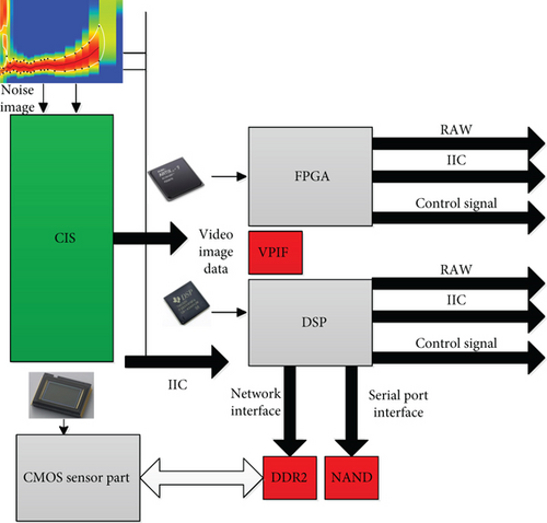
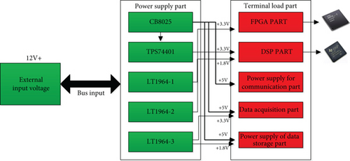
At the corresponding hardware level, we mainly focus on the selection of fpga+dsp architecture. Based on this, the FPGA and DSP selected in this paper are Selins’ A7 series and TI series, respectively. The control communication between the corresponding DSP and FPGA is realized through IIC bus, and the corresponding upper computer software communicates with DSP through serial port and corresponding network interface. In the corresponding system storage part, in addition to using the memory of the hardware processing system, it also includes DDR2 storage system. In the corresponding power management part, the power supply architecture adopted in this paper is distributed power supply. Its mainstream voltage includes 3.3 V, 1.8 V, and 5 V. The corresponding FPGA main power supply voltage is 1.8 V and 3.3 V. The voltage needs to be converted by 5 V. The corresponding DSP main power supply voltage is 3.3 V, which is also converted by 5 V. Based on this, 74401 is selected as the corresponding voltage conversion chip, which has the advantages of small size and high efficiency. The corresponding power supply architecture is in Figure 4. It shows the power supply and the corresponding voltage power on sequence. The corresponding power on sequence is designed as MCU>DDR>IO. The security of the system is ensured through the setting of power on sequence.
In the corresponding system software part, it mainly involves the design of video image excitation generator, video image filtering module, and communication module. In the design of video image excitation generator, we mainly focus on the timing of control signal and the solution of clock signal, register design, control signal, and so on. In the design of the corresponding image and video filtering module, the design based on on-off weighted median filtering algorithm is the main core. At the corresponding communication design level, the design is mainly based on UART modules, and the corresponding communication modules need to be verified. The corresponding verification platform is designed as a verification platform architecture based on UVM, which mainly organizes the operation of each verification component through a tree structure. In order to ensure the good operation of the verification platform architecture, test incentives need to be added, and before the actual test run, it is ensured that it can transmit data through a variety of baud rates. At the same time, it supports parity, duplex operation, real-time data receiving, and sending and supports the corresponding loop test analysis.
4. Experimental Verification
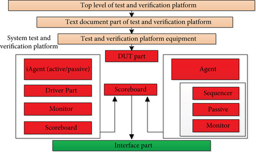
The corresponding experimental design platform is built. The corresponding platform architecture is shown in Figure 5. The top-level architecture of the corresponding verification platform is the top layer, and the corresponding internal module includes the operation entry module. The corresponding top layer will complete the instantiation of environmental problems such as clock signal processing, reset, and incentive testing. Based on this, this paper analyzes the comparative data. The main comparative analysis indicators include the comparative analysis of the performance indicators of the image and video acquisition system, the comparative analysis of the image and video filtering part, and the comparative analysis of the system operation efficiency. The corresponding experimental part of this paper mainly compares and analyzes the following three indicators: the number of iterations per unit time: it is mainly used to reflect the performance of the algorithm. The more the number of iterations, the higher the performance. Performance index of image and video acquisition system filtering algorithm: it is mainly used to reflect the filtering performance of the algorithm. Efficiency performance index of image and video acquisition system: it is mainly used to reflect the acquisition efficiency of the system image and video acquisition system.
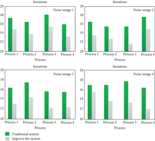
The first is the comparative analysis of the performance indicators of the image and video acquisition system. The main comparative analysis indicators include the comparative analysis of the number of iterations of the same video image processing to a certain extent. Based on the processing and analysis of four pictures in this paper, the comparative analysis of the number of iterations in this paper and the number of iterations in the traditional acquisition system are shown in Figure 6. The image and video data acquisition algorithm adopted in this paper has obvious advantages in the number of iterations in the processing of the same image compared with the traditional data acquisition scheme, so the corresponding system energy consumption is also reduced proportionally.
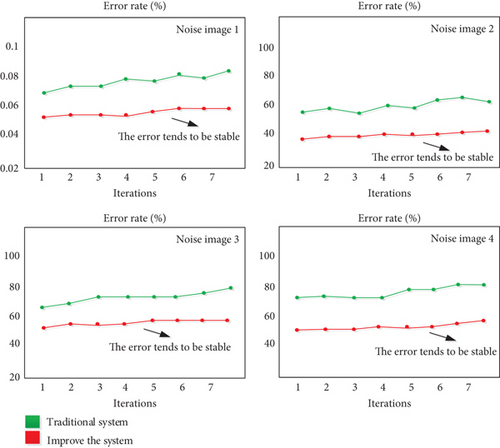
In the corresponding filtering quality comparison level, it mainly processes and analyzes an 8-bit standard gray-scale image. In this experiment process, the corresponding experiment is mainly divided into two steps. Firstly, noise detection is carried out, and impulse noise filtering is carried out based on noise detection. In the corresponding noise detection stage, the random noise has the greatest impact on the image quality, and the corresponding noise pixel has little difference with the corresponding gray value of the corresponding neighborhood pixel, which will cause the problem of missing detection of impulse noise. The corresponding Figure 7 shows the comparison curve of noise detection results corresponding to different iteration times under the same feature map. The experimental results show that the detection error rate of the on-off median noise filtering algorithm is smaller than that of the traditional monitoring scheme, and it tends to be stable faster.
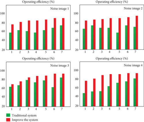
At the efficiency verification level of the corresponding video image data acquisition system, it mainly verifies the corresponding performance of the UART module. Based on this, this scheme is compiled and then simulated for this verification platform. The corresponding experimental process of this part is carried out under the Linux system. During the specific experiment, the corresponding incentive files need to be properly added to the verification platform; at the same time, the files contained in the corresponding verification platform need to be executable binary files. According to the above experimental process, the efficiency comparison and analysis curve of the corresponding image and video data acquisition system is shown in Figure 8. It can be seen from the analysis in the figure that the corresponding acquisition system scheme in this paper has performance advantages over the traditional scheme.
Based on the above experimental results and analysis, it can be concluded that the proposed video image data acquisition and analysis scheme has obvious advantages in performance, filtering quality, and corresponding system efficiency compared with the traditional scheme. Therefore, the scheme proposed in this paper has practical value and further promotion research value, which is of great significance to further improve the image and video processing technology.
5. Conclusion
This paper is mainly aimed at the disadvantages of the traditional image acquisition system, based on the visual intelligent sensor with CMOS image sensor as the core technology and optimizing its image data processing algorithm, which greatly improves the performance of the image acquisition system designed in this paper. At the specific research level, this paper mainly completes the hardware design of the image acquisition and transmission system based on the visual intelligent sensor produced and developed by a semiconductor company. In addition to the core processor of the system, this paper will also use audio and video processing chips and image data processing chips for collaborative analysis, so as to ensure the processing capacity and processing quality of the image acquisition system at the hardware design level. At the corresponding system software level, in order to further improve the quality of video signal processing, this paper proposes an on-off weighted median filter denoising algorithm, which has a significant effect on the processing of random impulse noise in video and the overall image filtering. At the same time, it also well protect the edge details of video image, so as to improve the authenticity of image and video. Based on this, this paper has built a verification platform based on supporting hardware and corresponding algorithms. Through hardware debugging and system operation analysis, when the operating frequency of the visual intelligent sensor is 100 MHz, the set acquisition depth is 10 bits, and the corresponding system collects data at a rate of 251 fps per second. In this case, the image acquisition system works stably. The corresponding restoration degree of the video image is higher, and the image transmission quality is higher. In the follow-up research, this paper will focus on the efficiency of the algorithm, solve the collection efficiency of the algorithm in the complex sampling environment, and reduce the corresponding energy consumption as much as possible.
Conflicts of Interest
The authors declare that they have no known competing financial interests or personal relationships that could have appeared to influence the work reported in this paper.
Acknowledgments
This work was supported by the Natural Science Foundation of Anhui Province: Research on substation temperature detection based on Intelligent Data Fusion (No.: KJ2020A0814).
Open Research
Data Availability
The data used to support the findings of this study are available from the corresponding author upon request.


