New Proposal for MCML Based Three-Input Logic Implementation
Abstract
This paper presents a new proposal for three-input logic function implementation in MOS current mode logic (MCML) style. The conventional realization of such logic employs three levels of stacked source-coupled transistor pairs. It puts restriction on minimum power supply requirement and results in increased static power. The new proposal presents a circuit element named as quad-tail cell which reduces number of stacked source-coupled transistor levels by two. A three-input exclusive-OR (XOR) gate, a vital element in digital system design, is chosen to elaborate the approach. Its behavior is analyzed and SPICE simulations using TSMC 180 nm CMOS technology parameters are included to support the theoretical concept. The performance of the proposed circuit is compared with its counterparts based on CMOS complementary pass transistor logic, conventional MCML, and cascading of existing two input tripple-tail XOR cells and applying triple-tail concept in conventional MCML topology. It is found that the proposed XOR gate performs best in terms of most of the performance parameters. The sensitivity of the proposed XOR gate towards process variation shows a variation of 1.54 between the best and worst case. As an extension, a realization of 4 : 1 multiplexer has also been included.
1. Introduction
MCML style finds application in communication systems, optical fiber links, digital to analog converter, microprocessors, and signal processors [1–3]. As compared to static CMOS logic, MCML has several advantageous features such as improved signal integrity, reduced power consumption, better power delay product at high frequencies, stability with technology generations, and improved security in cryptography applications [4–9]. A MCML gate consists of three main parts, namely, a pull down network (PDN), a current source, and a load. The PDN implements the logic function; the current source generates the constant bias current while the load performs the current-to-voltage conversion.
The logic function is realized using series-gating approach which suggests stacking of the source-coupled transistors pairs in the PDN. The number of stacked levels has a direct correspondence with number of inputs in the logic function. As the number of inputs becomes larger, there is increase in the number of stacked levels (NSL). For proper operation of MCML gate, a minimum power supply is required which is decided by the value of NSL and higher NSL result in larger minimum power supply. This serves as a main motivation behind using low voltage topology as lower power supply will result in reduced power consumption since the latter is computed as the product of bias current and power supply. Few low voltage techniques are available in the open literature [10–16]. The techniques [10–13] provide single ended output. A NOR based logic realization is proposed in [10, 11] to avoid stacking but it requires multistage realization of logic function. Additional current mirror, voltage, and current source are employed in [12, 13] to avoid stacking. The triple-tail cell concept is introduced in [14–16] to reduce NSL by one for the two-level MCML gates implementation. This paper introduces a new methodology for reducing the value of NSL by two and presents a quad-tail cell for this purpose. This method therefore allows three-input logic function realization using single level of source-coupled pairs and ultimately resulting in significant reduction in minimum power supply. A total of four proposed quad-tail cells are used for three-input logic function. The outlined method is generic in nature and can be applied to realize any three-input function.
The paper first discusses the basic realization of the three-input logic function in MCML style in Section 2. XOR gate is chosen for the purpose. Thereafter, Section 3 presents the new quad-tail cell put forward and its usefulness is illustrated through MCML XOR gate realization. The operation of the proposed XOR gate is explained and analytical formulations for the minimum power supply and voltage swing are put forward. Its performance comparison with the CMOS complementary pass transistor logic (CPL) based XOR gate, traditional MCML topology, and the two additional topologies is included in Section 4. A discussion on the general approach for implementing complex logic function in MCML style is also included. Extensive SPICE simulations are carried out to validate the proposed theory. Section 5 concludes the paper.
2. Conventional Three-Input MCML Gate Realization
The basic architecture of MCML gate consists of a pull down network (PDN), a current source, and a load as shown in Figure 1(a). The PDN implements the logic function, the current source maintains a constant bias current, and the load performs the current-to-voltage conversion [4]. The gate works on the principle of current steering. Depending upon the inputs, the bias current is steered to one of the output branches and produces the output accordingly. The logic function is realized by using series-gating approach [17]. It is a systematic and a general approach wherein a logic function is implemented as a network of source-coupled transistor pairs having all transistor paths associated with the possible input combinations and then properly connecting each of the upper drain nodes to the output nodes. Based on this, the schematic of MCML XOR gate with differential inputs A, B, and C is shown in Figure 1. The PDN has three levels of source-coupled transistor pairs (M2–M15), the load transistors (M16, M17), and a constant current source M1 that generates the bias current ISS. The differential inputs A, B, and C drive the uppermost (M8–M15), middle (M4–M7), and lowest (M2-M3) levels, respectively. Consider, for instance, that all the inputs are high. Under this condition, the bias current is steered in transistors M2, M4, and M9 such that high and low voltages are obtained at the nodes Q and through the load transistors.

3. The Proposal
A new approach to realize three-input MCML gate is presented in this section. The realization employs a novel circuit element named quad-tail cell to reduce the number of source-coupled transistor levels.
3.1. Quad-Tail Cell
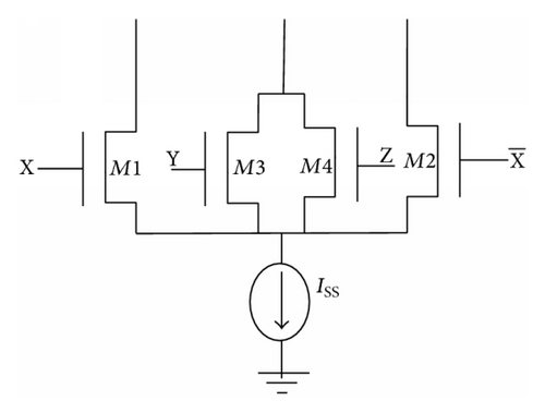
A quad-tail cell is an extension of the triple-tail cell concept [14–16] and consists of four source-coupled transistors (M1–M4) as shown in Figure 2. In the cell, the activation/deactivation of the two outer transistors (M1, M2) is controlled by the two internal transistors (M3, M4). To elaborate this, consider when either one input among Y and Z is high or both these inputs assume high value. Under these circumstances, the current ISS is steered through transistors M3 or/and M4; and the transistors M1 and M2 remain deactivated. Conversely, if both the inputs Y and Z are low, the current ISS will steer to one of the two transistors (M1, M2) depending upon the value of the input X. The requirement for the proper activation/deactivation of the quad-tail cell is similar to triple-tail cell; that is, the aspect ratio of internal transistors M3 and M4 should be larger than the others by a factor of N.
3.2. Proposed XOR Gate
A three-input XOR gate is considered to illustrate the use of quad-tail cell and its complete schematic is shown in Figure 3. It uses four quad-tail cells (Q1–Q4) each biased by current source of ISS/4 value. The inputs connection to the internal transistors of the quad-tail cells is done in a manner so that at any instance of time the outermost transistors in only one quad-tail cell get activated. To elaborate this further, consider that all the inputs A, B, and C are high. In this condition, the outermost transistors of only Q1 are activated while, for the rest (Q2–Q4), the bias current is steered to the internal transistors making deactivation of corresponding outermost transistors.
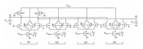
Case 1 (differential inputs B and C are high). In this condition, the outermost transistors of Q1 (M5-M6) are activated. For high value of differential input A, the transistor M5 is OFF and M6 is ON. Thus, their currents can be written as
At the same time, the quad-tail cells Q2–Q4 are deactivated via the turning ON of their respective inner transistors. But since the complete deactivation of the quad-tail cell cannot be achieved, therefore, small current still flows in the outer transistor of these cells which needs to be considered for calculating the differential output voltage. So, for given factor N, the current flowing in the transistors M7–M12 can be computed as
Substituting these current values in the output voltage expression, we get high differential output voltage (VOH) as
Similarly, the current through transistors M5–M12, for low value of the differential input A, is given as
Case 2 (differential inputs B and C are low). In this condition, the outer transistors (M11-M12) of Q4 are activated while those of Q1–Q3 (M6–M10) remain deactivated. For high value differential input A, the current through the transistors (M5–M12) can be written as
Substituting these current values in the output voltage expression (3), we get high differential output voltage (VOH) as
Similarly, for low value of the input A, the current through the transistors (M5–M12) can be written as
Substituting these current values in (3), we get low differential output voltage (VOL) as
Case 3 (differential input B is high and input C is low). In this condition, the outer transistors (M9-M10) of Q3 are activated while those of Q1, Q2, and Q3 (M5–M8, M11-M12) are deactivated. For high value input A, the current through the transistors (M5–M12) can be written as
Substituting these current values in the output voltage expression, we get low differential output voltage (VOL) as
Similarly, for low value of the input A, the current through the transistors (M5–M12) can be written as
Substituting these current values in (3), we get high differential output voltage (VOH) as
Case 4 (differential input B is low and input C is high). In this condition, the outer transistors (M7-M8) of Q2 are activated while those of Q1, Q3, and Q4 (M5-M6, M9–M12) are deactivated. For high value input A, the current through the transistors (M5–M12) can be written as
Substituting these current values in the output voltage expression, we get low differential output voltage (VOL) as
Similarly, for low value of the input A, the current through the transistors (M5–M12) can be written as
Substituting these current values in (3), we get high differential output voltage (VOH) as
From the above analysis, the voltage swing (VSWING_PG) of the proposed gate can be determined as
This indicates that the voltage swing of the proposed gate is smaller than the conventional MCML gate (see (1b)). So, in order to achieve the same voltage swing as the conventional MCML gate, the load resistance of the proposed gate (RP) is increased accordingly.
4. Simulations Results and Discussion
In this section, the functionality of the proposed three-input XOR gate is verified through simulations using 180 nm CMOS technology parameters. Its performance is compared with the conventional MCML XOR topology, two more MCML XOR circuits, and CMOS complementary pass transistor (CPL) based XOR topology for the sake of fair comparison. Both the MCML topologies use triple-tail concept to lower the number of source-coupled pair levels. The first topology employs a cascade of two input XOR gates while the second realization reduces the NSL from three to two. All the XOR gates are simulated with their respective minimum power supply and load capacitance of 50 fF. The MCML topologies are designed so that the total current drawn from the power supply is 100 μA and voltage swing is 400 mV. Further, the total current drawn from the power supply per gate is retained at 100 μA for MCML topologies while maintaining voltage swing of 400 mV. The performance comparison is done on the basis of power, propagation delay, power delay product (PDP), transistor count, gate count, and switching current. The simulation of a ring oscillator based on the proposed and the conventional XOR gate is performed for completeness. A discussion on the general approach for implementing complex three-input logic function is included.
4.1. Functional Verification of the Proposed Circuit
The functionality of the proposed quad-tail cell based three-input MCML XOR gate is verified through simulations with simulation conditions discussed above. The timing waveforms for differential inputs A, B, and C and the corresponding differential output are shown in Figure 4. It can be observed that differential output voltage is high for all the cases having odd number of high inputs and remains low otherwise. Thus, the proposed MCML XOR gate adheres to desired functionality.

4.2. Performance Comparison
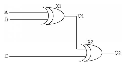
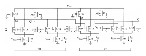
The performance of the proposed XOR gate is compared with the conventional three-input XOR gate (Figure 1). To give broader perspective, two more possible three-input XOR gate circuit realizations are also included. Both realizations use triple-tail concept to lower the number of source-coupled pair levels. The first realization is derived from the fact that the three-input XOR gate functionality can be achieved by cascading the two input XOR gates as shown in Figure 5(a). The inputs A and B are connected to XOR gate X1 while its output and the input C are fed to XOR gate X2. The recent implementation of the two input XOR gates [14–16] is chosen for implementation. The complete MOS based schematic of the three-input XOR gate is shown in Figure 5(b) and is referred to as Topology 1 in the context of the paper.

- (i)
The power supply constraint for proposed XOR gate and Topology 1 is same whereas conventional topology needs largest value and requirement for Topology 2 lies in the middle. This is a direct consequence of presence of NSL; for example, topologies (proposed topology and Topology 1) employ single level while conventional topology and Topology 2 use three and two levels, respectively.
- (ii)
Since all the topologies are designed to draw 100 μA current from the power supply, therefore the topologies (proposed topology and Topology 1) consume same power which is lower than the remaining two.
- (iii)
It is clear from above point that the topologies (proposed topology and Topology 1) consume the least power among those listed in Table 1. In terms of the propagation delay, proposed topology shows significant improvement which may be attributed to reduced number of stages. This accounts for lowest power delay product values (PDP).
- (iv)
Though gate count is equal for conventional topology, Topology 2, and proposed topology, the proposed topology performs best in terms of propagation delay, power, and PDP.
- (v)
The transistor count in proposed topology is highest among all.
- (vi)
The delay in MCML based conventional XOR gate and Topology 1 is comparatively higher than that in proposed topology and Topology 2. It is due to the fact that there are three stacked source-coupled transistors pair levels which contribute to large parasitic capacitance at the output node. The delay in Topology 1 is due to cascading of two XOR gates. Though the proposed topology and Topology 2 employ a single gate, parasitic contribution in latter topology is higher than former one. This explains lowest delay of the proposed XOR gate topology among all.
- (vii)
All the MCML based XOR gate topologies produce less switching current in comparison to CMOS CPL based due to the presence of constant current source. The results thus confirm the preference of MCML based topologies in low noise mixed-signal environments over the CMOS based counterparts [5, 19].
- (viii)
The CMOS CPL based XOR gate consumes the lowest power but shows high delay and PDP values in comparison to all MCML based XOR gate topologies. Therefore, it is not considered further in the proposal.
| Parameter | Circuit | ||||
|---|---|---|---|---|---|
Conventional MCML |
Topology 1 | Topology 2 | Proposed | CMOS CPL |
|
| Supply voltage (VDD) | 1.7 V | 1.1 V | 1.4 V | 1.1 V | 1.0 V |
| Power consumption (μW) | 170 | 110 | 140 | 110 | 44 |
| Propagation delay (ps) | 1178 | 1049 | 732 | 614 | 4017 |
| Power delay product (fJ) | 166.770 | 115.390 | 102.480 | 67.540 | 176.748 |
| Gate count | 1 | 2 | 1 | 1 | 1 |
| Transistor count | 17 | 20 | 18 | 22 | 18 |
| Switching current (μA) | 5 | 40 | 25 | 20 | 42 |
To examine the sensitivity of different XOR realization performance towards process variation, the propagation delay and the voltage swing obtained through simulations are comprehended in Table 2. The variation between the best and worst case in the propagation delay is by a factor of 1.63, 1.29, 1.48, and 1.54, respectively, for conventional topology, Topologies 1 and 2, and the proposed one. Analogously, the corresponding factors for voltage swing are 2.19, 2.28, 2.25, and 2.54 for conventional topology, Topologies 1 and 2, and the proposed one. The voltage swing values should be more than 1.4 Vdssat, where Vdssat is the saturation drain-source voltage of the differential transistor pair for functionality to remain intact [20]. It may further be noted that the proposed MCML gates can maintain constant voltage swing against process variation by modifying their load section by using adaptive bias controller as suggested in [21, 22].
| XOR gate topology | NMOS | T | F | S | F | S |
|---|---|---|---|---|---|---|
| PMOS | T | F | S | S | F | |
| Propagation delay (ps) | ||||||
| Conventional | 1178 | 976 | 1586 | 1091 | 1417 | |
| Topology 1 | 1049 | 971 | 1253 | 1071 | 1126 | |
| Topology 2 | 732 | 627 | 930 | 723 | 806 | |
| Proposed | 614 | 430 | 664 | 659 | 661 | |
| Voltage swing (mV) | ||||||
| Conventional | 400 | 444 | 290 | 580 | 264 | |
| Topology 1 | 400 | 434 | 286 | 572 | 250 | |
| Topology 2 | 400 | 454 | 296 | 576 | 256 | |
| Proposed | 400 | 424 | 298 | 550 | 216 | |
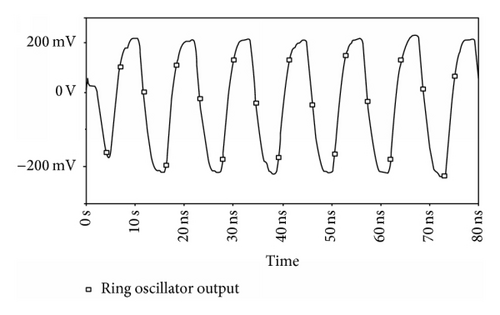
The behavior of proposed XOR gate is also investigated by configuring it as an inverter and cascading five such inverters in a loop to obtain five-stage ring oscillator (RO). The timing waveform is shown in Figure 7. RO is also constructed with conventional XOR gate with similar connections. It also gives oscillations and timing waveform is similar to that of Figure 7 which is omitted for the sake of brevity. To verify the functionality of RO constructed with proposed and conventional topologies at all PVT corners, a number of simulations have been performed and the results are comprehended in Table 3. It can be observed that the oscillations are achieved at all the process corners and the values exhibit the same trend as shown in Table 2 for individual gate simulation.
| Topology | NMOS | T | F | S | F | S | T | T | T | T |
|---|---|---|---|---|---|---|---|---|---|---|
| PMOS | T | F | S | S | F | T | T | T | T | |
| T (°C) | 70 | 0 | 125 | 70 | 70 | 70 | 70 | 0 | 125 | |
| Conventional | ||||||||||
| VDD (V) | 1.7 | 1.87 | 1.53 | 1.7 | 1.7 | 1.87 | 1.53 | 1.7 | 1.7 | |
| Freq. (MHz) | 95 | 108 | 65 | 71 | 66 | 100 | 59 | 125 | 77 | |
| Proposed | ||||||||||
| VDD (V) | 1.1 | 1.21 | 0.99 | 1.1 | 1.1 | 1.21 | 0.99 | 1.1 | 1.1 | |
| Freq. (MHz) | 140 | 181 | 114 | 125 | 139 | 147 | 90 | 163 | 125 | |
The theoretical and simulated values for this ratio are 7.68 and 9, respectively. Thus, the proposed topology is less power efficient if the parasitic contribution of the transistors in the two XOR gate topologies is made equal.
4.3. A Generalized Approach
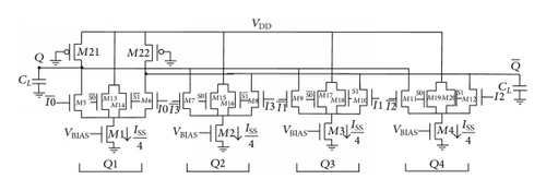
The proposed quad-tail cell can be used to formulate a general design approach for logic function realization. Four numbers of quad-tail cells can be connected in a configuration given in Figure 8 to realize a 4 : 1 multiplexer. The input lines are marked as I0–I3, and select lines are denoted by S0 and S1. The four input lines (I0, I1, I2, and I3) form the input to the outer transistors of the quad-tail cells (Q1, Q2, Q3, and Q4), respectively, while select lines are tied to inner transistors according to the operation. The availability of the desired input line at the multiplexer output can be achieved by proper activation of the quad-tail cell through select lines S0 and S1. For instance, the data on the input line I1 can be made available at the output of the multiplexer for low and high values of S0 and S1, respectively. It is well known that any three-input logic function can be implemented using 4 : 1 MUX so the circuit of Figure 8 can practically realize (23)2 logic functions. The mapping table for I0–I3 and S1-S0 is omitted for the sake of brevity.
5. Conclusion
A new proposal for three-input logic function realization in MCML style is presented. The new proposal reduces the number of stacked source-coupled transistor levels in the logic function realization. A circuit element named quad-tail cell is presented for this purpose and its use in the implementation of three-input exclusive-OR (XOR) gate is elaborated. Its behavior is analyzed and SPICE simulations using TSMC 180 nm CMOS technology parameters are included to support the theoretical concept. The performance of the proposed circuit is compared with the conventional XOR topology along with two more triple-tail cell based topologies. Comparison with CMOS complementary pass transistor logic based XOR gate is also included for the sake of completeness. The performance of all XOR gate realizations is compared and it is found that the proposed XOR gate topology performs best in terms of most of the performance parameters. The sensitivity of different MCML XOR gate realization performance is examined towards process variation which indicates similar values. A discussion on the realization of three-input logic by configuration of a 4 : 1 multiplexer has also been included as an extension of the work.
Competing Interests
The authors declare that they have no competing interests.


