Rootlike Morphology of ZnO:Al Thin Film Deposited on Amorphous Glass Substrate by Sol-Gel Method
Abstract
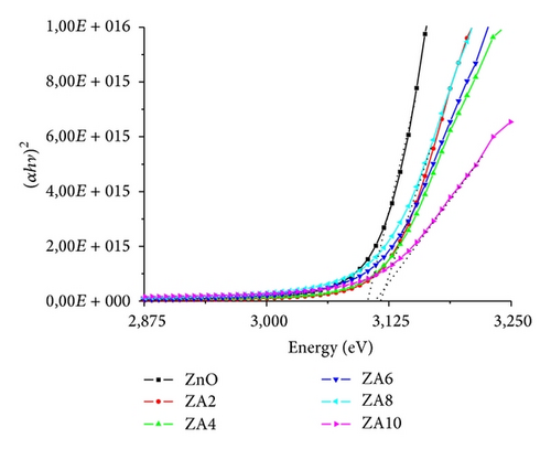
Zinc oxide (ZnO) and aluminum doped zinc oxide (ZnO:Al) thin films have been deposited onto a glass substrate by sol-gel spray coating method at atmospheric pressure. X-ray diffractometer (XRD), scanning electron microscopy (SEM), and UV-Vis spectrophotometer have been used to characterize the films. XRD spectra indicated that all prepared thin films presented the wurtzite hexagonal structure. SEM images exhibited rootlike morphology on the surface of thin films and the shortest root diameter was about 0.219 μm. The UV-Vis absorption spectra exhibited the absorption edges that were slightly shifted to the lower wavelength. From this result, the incorporation of aluminum into the ZnO involved a slight increase in the optical band-gap of films. The optical bands of films were 3.102 eV, 3.115 eV, 3.118 eV, 3.115 eV, 3.109 eV, and 3.109 eV for ZnO, ZnO:Al 2%, ZnO:Al 4%, ZnO:Al 6%, ZnO:Al 8%, and ZnO:Al 10%, respectively. Increase of Al doping concentration in ZnO films contributed to the increase of their optical band-gap which can be explained by the Burstein-Moss effect.
1. Introduction
Zinc oxide (ZnO) is the most popular materials that can be used for many applications. Many researchers have studied this material for electronics [1], energy [2], and environment [3] applications. ZnO is of low cost and nontoxic and has high chemical stability which make this material so interesting [4]. ZnO can be used for transparent conductive oxide [5], gas sensors [6], and photocatalyst [7–9]. ZnO has a wide band-gap energy (~3.3 eV) and has been studied in different forms such as powder [10] and thin film [11]. Several techniques can be used to make ZnO:Al thin film, such as DC or RF magnetron sputtering [12, 13], electron beam evaporation [14], pulsed laser deposition [15], chemical vapor deposition [16], spray pyrolysis [17], and sol-gel processing [18]. Sol-gel is the most widely used method because of its easy and low-cost preparation [19].
Substitution of Zn2+ ion by group III ions such as B3+, Al3+, Ga3+, and In3+ will produce extra electrons and improve optical, electrical, thermal, and magnetic properties. The most commonly used dopant is aluminum (Al) [20, 21]. In this work, we proposed ZnO and ZnO:Al thin films deposited by sol-gel spray coating. The films have been characterized by XRD, SEM-EDX, and UV-Vis. The Al doping concentration in the ZnO:Al films was controlled and its effect on the films properties was investigated.
2. Materials and Method
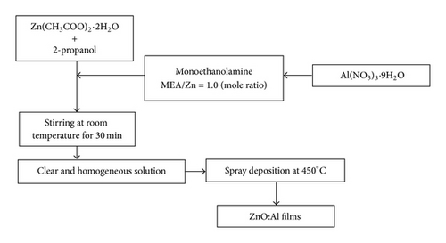
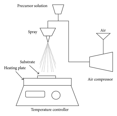
ZnO and ZnO:Al thin films were synthesized by sol-gel spray coating method. As a starting material, zinc acetate dihydrate (Zn(CH3COO)2·2H2O) was dissolved in 2-propanol with a concentration of 0.5 mol L−1. Monoethanolamine (MEA) was wisely dropped into solution and was stirred under room temperature for 30 min. For doped films, aluminum nitrate nonahydrate (Al(NO3)3·9H2O) was added to the solution with a molar percentage, fixed at 0, 2, 4, 6, 8, and 10% moles and were then denoted as ZnO, ZA2, ZA4, ZA6, ZA8, and ZA10, respectively. The precursor solution was deposited onto glass substrate by spray coating at 450°C hotplate temperature and allowed for 1 hr. Figure 1(a) showed the flow chart of preparation and (b) diagram of spray coating system that was used in this study. Prior to a deposition, the glass substrate was cleaned by ultrasonic cleaner using acetone, methanol, and bidistilled water. The prepared thin films were characterized by X-ray diffraction (XRD) using Shimadzu Maxima 7000 (Cu-Kα wavelength: 1.5405 Å). The detection angles were ranging from 2θ = 10 to 90°. The morphology of thin films was shown by scanning electron microscopy (SEM) and energy dispersive X-ray spectroscopy (EDX) using JEOL-JSM 6510 LA. The optical transmission of the films was measured by a UV-Vis spectrophotometer (Shimadzu 1240 SA).
3. Results and Discussion
3.1. Microstructure
| Sample name | 2θ (002) | FWHM (deg) | D (nm) | c (Å) |
|---|---|---|---|---|
| ZnO | 34.42 | 0.45816 | 18.85 | 5.206797 |
| ZA2 | 34.48 | 0.36741 | 23.52 | 5.198011 |
| ZA4 | 34.42 | 0.44695 | 19.33 | 5.206797 |
| ZA6 | 34.44 | 0.33876 | 25.50 | 5.203865 |
| ZA8 | 34.42 | 0.34697 | 24.90 | 5.206797 |
| ZA10 | 34.44 | 0.34048 | 25.37 | 5.203865 |
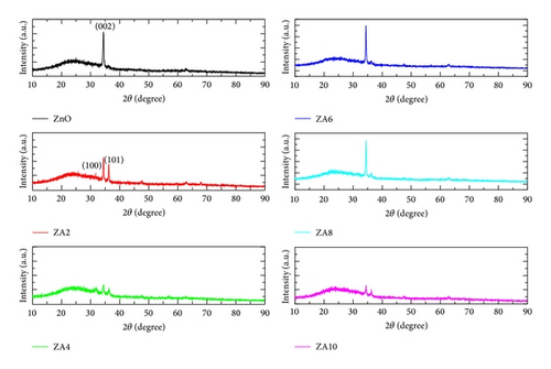
We can note that the lattice parameter c decreased; it might be affected by the substitutional replacement of Zn2+ (ionic radius 0.072 nm) ions by Al3+ (ionic radius 0.053 nm) [23]. The estimated value of crystallite size from (002) plane was found to increase from 18.85 nm for ZnO to 25.37 nm for ZA10. Normally, it was expected that the crystallite size should also decrease due to replacement of Zn2+ ions by Al3+ ions [24]. The same result has been obtained by Abd-Lefdil et al. [25]. The increase in crystallite size may be due to the enhanced thickness of Al-doped films. During deposition process, the lower surface energy grains may become larger as film thickness increase [26].
3.2. Morphology
Figure 3 represents the SEM observation of all prepared samples. It can be seen that all films have rootlike morphology. In ZnO image, the root surface had the longest diameter of all other samples. ZnO:Al thin films had shorter root diameter and the shortest root diameter was obtained by ZA6. The root diameter was shown in Table 2. The rootlike morphology was rarely found in other ZnO thin film studies.
| Sample name | Root diameter (µm) | Al/Zn in solution | Al/Zn incorporated | Energy gap (eV) |
|---|---|---|---|---|
| ZnO | 0.482 | 0 | 0 | 3.102 |
| ZA2 | 0.227 | 0.02 | 0.01 | 3.115 |
| ZA4 | 0.377 | 0.04 | 0.02 | 3.118 |
| ZA6 | 0.219 | 0.06 | 0.03 | 3.115 |
| ZA8 | 0.375 | 0.08 | 0.03 | 3.109 |
| ZA10 | 0.288 | 0.10 | 0.03 | 3.109 |
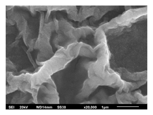
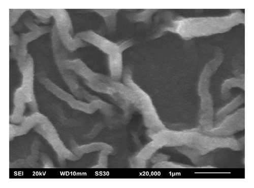
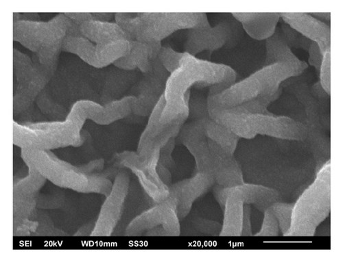
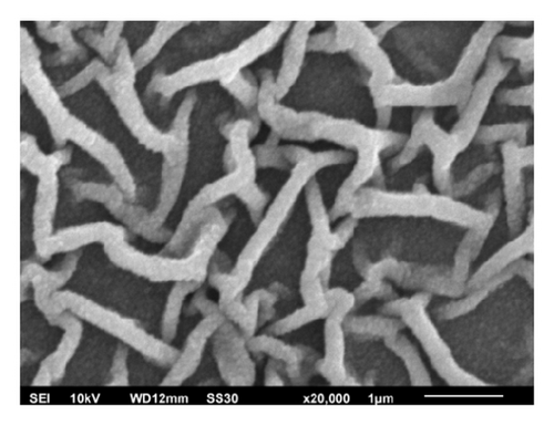
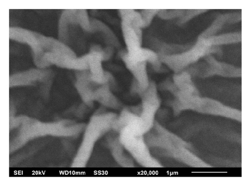
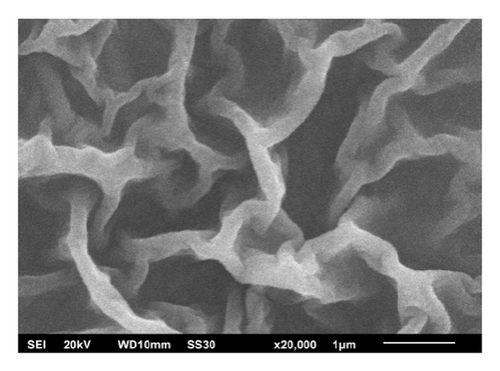
Figure 4 depicts the suggested ZnO growth mechanism using sol-gel spray coating method at 450°C. During deposition, the layer of crystalline grains is built onto glass substrate. There is a different temperature from the first layer and other layers that affects the interaction among them. Many particles merge with other particles to make a long structure of ZnO which is called rootlike morphology.

EDX result exhibited Al composition in the thin film sample which was different from Al composition in the precursor solution as shown in Table 2. This might be caused by only a small percentage of Al ions that enable substituting Zn ion. Another reason was the high loss of Al during spray deposition. We can see the saturation result of Al/Zn incorporation at higher percentage of Al doping. This result was affected by the limitation of Al doping in ZnO thin film. The thermodynamic solubility limit of Al in ZnO has been reported to be in the 2-3 at. % range [27]. According to the phase diagram of Al/Zn mixture in the previous study [28], the mixture only shows Zn phase at our temperature treatment. The limitation of Al is the maximum Al content in the ZnO at a given temperature. The substitution of Al in ZnO remains quite difficult because of the difference in ionic radius, coordination preference, and oxidation state [29].
3.3. Optical Properties
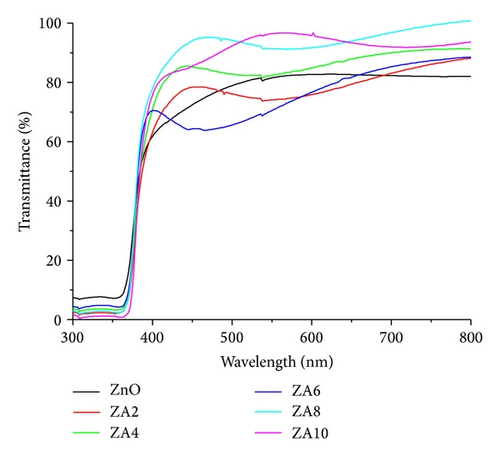
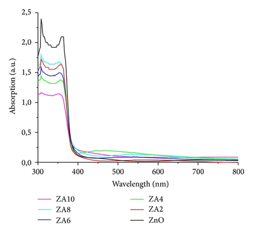
The optical transmittance spectra were shown in Figure 5 and, in these spectra, an improvement of the film transparency at high Al doping concentration can be seen. The highest transparency was obtained by ZA8 about 95% in the visible wavelength region. The increase can be explained by the reduction of light scattering in the film which was caused by the lower thickness [18]. It also exhibited the fringes pattern that indicated the high quality and homogenous surface [30]. Figure 6 shows the absorbance spectra of all prepared thin films. We can see that ZnO:Al thin films have a slight shift to lower wavelength (blue shift).
The optical band-gap of ZnO and ZnO:Al thin film was presented in Figure 7. The ZnO:Al thin films had bigger optical band-gap than pure ZnO thin film; the same result has been obtained by some papers [32–35]. The increase of band-gap was caused by the Moss-Burstein effect [36]. The effect stated that the blue shift of the optical band-gap of semiconductors is affected by impurity in the conduction band [37]. ZnO:Al films are semiconductors in which the Fermi level lies in the conduction band which means that electrons occupy the levels at the bottom of the conductivity band [37, 38].
4. Conclusions
The pure and the aluminum doped ZnO films were successfully deposited by the sol-gel spray coating technique. XRD spectra showed the hexagonal wurtzite structure of ZnO. The estimated crystallite size increases with addition of Al due to replacement of Zn2+ ions by Al2+ ions. The surface of all prepared thin films showed rootlike morphology and the diameter decreased with increase of Al content. The transmittance spectra showed high transparency of ZnO:Al thin films about 95%. The absorbance spectra exhibited that ZnO:Al had a slight shift to higher wavelength than pure ZnO. The optical band-gap resulted in slight increase for the Al-doped films as explained by the Moss-Burstein effect.
Competing Interests
The authors declare that there is no conflict of interests regarding the publication of this paper.
Acknowledgments
The authors would like to thank The Ministry of Research, Technology and Higher Education, Indonesia, through Competence Grant 2016 for funding of this work.


