High Efficiency Driver for AMOLED with Compensation
Abstract
A new proposed compensation driver circuit of flat-panel display (FPD) based on organic light emitting diodes (OLEDs) and on poly-crystalline silicon thin-film transistors (poly-Si TFTs) is presented. This driver circuit is developed for an active-matrix organic light-emitting-diode (AMOLED) display and its efficiency is verified compared with the conventional configuration with 2 TFTs. According to results, this circuit is suitable to achieve acceptable level for power consumption, high contrast, maximum gray levels, and better brightness. And, to show this, a stable driving scheme is developed for circuit with much compensation such as against the data degradation, the threshold voltage dispersions of TFT drive, and suppression of TFT leakage current effect.
1. Introduction
The new generation of display, organic electronic display, based on organic light emitting diodes (OLEDs) has established to eliminate the defects reported for the other technologies (LCD and PLASMA): low contrast and high consumption [1, 2] with speed conditions that may be unacceptable for some displays of 3 dimensions due to addressing type. This new technology meets the needs of users in terms of pure picture quality and functioning level especially for mobile devices; it offers new possibilities previously unattainable as the deposition on large surfaces or on flexible substrates because of low temperature of the OLED treatments [3, 4]; also the vision affects reality in terms of quality. On the other hand, the current driven of OLED device can be provided by a passive matrix or active matrix backplane architecture [5]. In the latter case the colour adjustment is determined by a command based on thin film transistor (TFT) [1, 5]. This solution is preferred, especially when the size of the display increased where we have technical problems [6]. The backplane of the active matrix is like a group of switchers or circuits which controls the current intensity flowing through each OLED pixel and does not let electricity only when this is necessary. These circuits’ designs are based on amorphous silicon (a-Si) [7], polycrystalline silicon (poly-Si) [2], organic TFT (O-TFT) [8], and circuits’ designs complementariness. According to the manufacturers, several technologies backplanes in terms of structure and level of fitness, which are used for uniformity and stability sufficient for brightness which differ in their driving speed, power consumption, area occupied, and the accuracy needed to set the current level, have been presented. In particular, these driver circuits can be classified into two programming modes in accordance with the data type: voltage-programming circuit and current-programming circuit [6]. However for both types of circuits at the driving scheme, the variations in threshold voltage of TFTs, due to the change in mobility under the influence of operating time and under abnormal thermal conditions which can attain, respectively, 10% to 50%, the data degradation, and the change in supply voltage, the leakage current [9], and the speed, generate degradation and nonuniformity in brightness over time in the pixel itself and in many cases there is a fluctuation in brightness in the surrounding pixels. These disturbances add up over time and may be the cause of poor vision. To avoid these problems, the manufacturers are using these transistors with adequate compensation methods [5]. Nevertheless, high-quality displays, low power consumption, and improvement of the nonuniform brightness and the efficiency of the driver circuits require several driving transistors per pixel to allow compensation for major technical problems. Specifically using compensation circuits based on poly-Si technology has been a considerable progress in providing stable and uniform brightness with great lifetime. Also it is not cost-effective in comparison with other TFT technologies (a-TFT and O-TFT) and it can provide constant current to OLED and excellent mobility; compensation circuits reached the requirements of OLED driving current under minimum power supply respecting the speed condition and also assists in the direct integration of the driver circuit on the flexible substrates [2, 5–7, 10]. In this paper we privilege the use of poly-Si transistor for the proposed driver circuit. And generally we can say that the choice of one of these transistors is closely related to the manufacture which has its own parameters and its driving schemes and the technology used to make the AMOLED screen.
2. The Proposed Driver Pixel Circuit
As we have said before, we have chosen the use of poly-Si for the proposed driver circuit. And to ensure high speed; it will be preferable to use N-type transistors rather than P-type. Also for applications of high frequency, it is better to use those of N-type instead of P-type. For these reasons we chose using an N-type transistor as a scan transistor. And for application, we use enrichment MOSFET models thanks to the performances that they give especially under abnormal thermal conditions. The proposed design is explained compared with the conventional circuit based on 2-TFTs, Figure 1(a) [6, 8, 11].
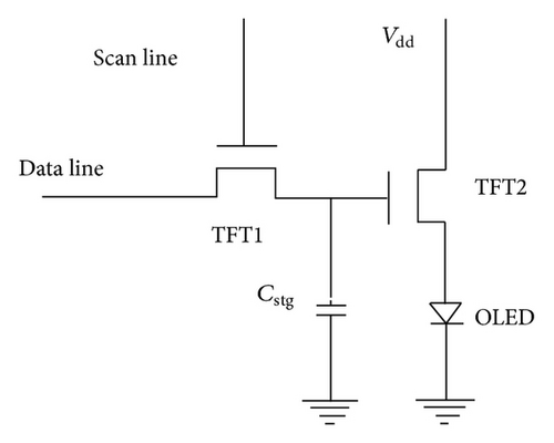
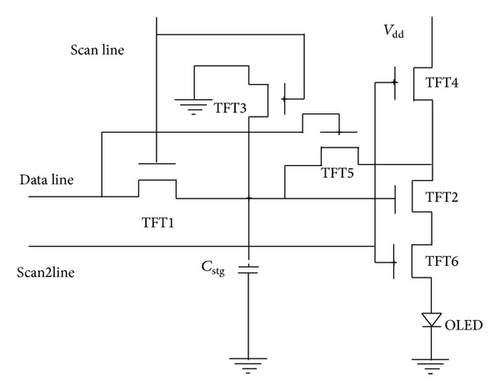
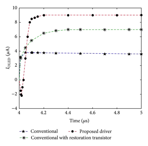
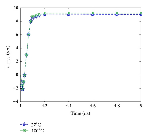
Firstly, to well compensate the loss in data voltage, we add another transistor of P-type: a restoration transistor TFT3, Figure 1(b). With this transistor, the charge stored in the capacity is exactly the data voltage, but the most important issue is the size of this restoration transistor. In reality, it acts as capacitance, and their limited size is directly related to the loading time of Cstg with TFT1 and their internal capacitance, Cgb (gate-bulk capacitance); this is a very important condition for calculating their capacitance. Therefore, this transistor provides a load current in capacitance Cstg and decreases the charging time to make it equal to the time of loading capacitance Cstg through TFT1, so it must reduce its internal resistance (Rsh: drain, source diffusion sheet resistance), resulting from an increase in their ratio WTFT3/LTFT3. Subsequently we have two conditions that must be respected: we increase W/L to reduce the resistance and we increase W × L to increase the internal capacitance, Cgb, of this transistor. The optimal values that allow us to offset the data degradation are threshold voltage VTh-TFT3 = −VTh-TFT1 and W = 4 × L. In this condition, the maximum current delivered to the OLED becomes 7 µA; see Figure 2, and therefore we have successfully corrected the data degradation and increase the current IOLED. In addition, despite the compensation of the data degradation, we have always the problem of threshold voltage variation of TFT2 with increased energy consumption due to the presence of anther capacitance which is represented by the transistor TFT3. So we seek a method to resolve these problems. First, to minimize power consumption, the OLED is active only if necessary. For this a new transistor of P-type, TFT4, ordered by a new control line, Scan2line, is added as shown Figure 1(b); this transistor does not leave the driver circuit works only if that is necessary even if the VData is already stored in the capacitance Cstg. Second, to avoid the problem of the threshold voltage variation of TFT2, we add another transistor of P-type, TFT5, Figure 1(b). The simulation gives an increase in the maximum current to 9 µA; see Figure 2. This increase of 2 µA is due in fact to the storage of the threshold voltage VTh-TFT2 of TFT2 in the capacitance Cstg. Moreover the presence of leakage current in the OLED during the reset phase requires us to add another transistor to eliminate it, because this current becomes critical for the lifetime of OLED so in screen over time where the screen colours will become darker if we exceed certain hours of operation and has a direct effect on the contrast and on the stored charge in Cstg [9]. So it must be reducing leakage current. To do this, we add another transistor, P-type TFT6, to block the emission current through the OLED during the reset phase and ensure greater stability for the pixel, Figure 1(b). Therefore, the final proposed driver circuit is able to reduce the problem of nonuniformity of brightness, it has a large output current with faster response time, it can block the current circulating in the OLED during the reset period where an increase in contrast ratio is guaranteed, and it reduces energy consumption. Also, the OLED is placed between the drain of TFT6 and the ground to cancel the transient characteristics. So we can say that the proposed circuit pixel is suitable for AMOLED screen, but it requires more precision by the insertion of the new control signal, Scan2line.
3. Driving Scheme
In the proposed design exposed in Figure 1(b) TFT1, TFT4, TFT5, and TFT6 function as switches, TFT3 is the restoration transistor, and TFT2 is the driving transistor; it operates in saturation regime when it is in the passant state. The timing or the driving scheme for this proposed driver is defined as shown in Figure 3. Figure 4 shows the operations steps with the main compensations. From these figures we find the following.
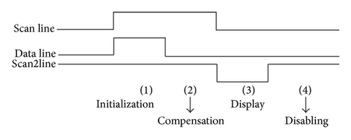
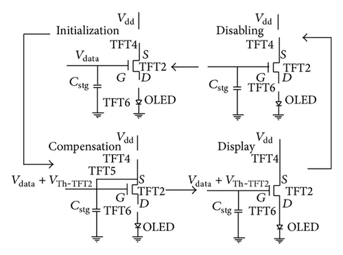
Compensation Phase of the Threshold Voltage of TFT2. During this phase the signal Scan2line is in the high state, TFT4 and TFT6 are blocked, and data line is in the low state to make the loading of the threshold voltage of TFT2 in the capacitance Cstg. At this time the gate of TFT2 is connected with their drain through the transistor TFT5, where we have a diode type connection, and so the voltage across the capacity Cstg becomes VData + VTh-TFT2. This technique allows cancelling the threshold voltage variation when the TFT2 commands OLED.
Disabling Phase. This is the nonoperation phase of the pixel. It is applied if we want to avoid the operation of the pixel. It is obtained by forcing the signal Scan2line to be in a high state, even in the case where we have a charge stored in the capacitance Cstg. This charge remains constant until the next reset phase.
4. Performances and Discussion
5. Conclusion
In this work, a new compensation driver circuit based on the technology TFT poly-Si as a support of the organic matrix thanks to its speed and its thermal stability is proposed with its driving scheme, consisting of 6 transistors TFTs and having three input lines (data line and scan line plus one additional control signal: Scan2line) plus one storage capacitance. By results of circuit tests, it is found that the proposed circuit can be successfully operated under optimal timing scheme; it offers a stable output current of high value while keeping a response time relatively fast compatible with the requirements of AMOLED displays under minimal power consumption and abnormal thermal conditions. We have shown for this proposed circuit a driving scheme based on restoration technique for the data degradation and compensation of the threshold voltage variation of TFT2 driver by using the method of loading this voltage in the capacitance Cstg. On the other hand, to reduce energy consumption, increase the contrast ratio, and suppress TFT leakage effect, we have introduced two other transistors with additional signal line to prevent the leakage current and to make this pixel operate as needed. This proposed circuit is compared with the conventional circuit of 2 TFTs, and we can simply say that it is very suitable for contrast, consumption, speed, and stability of brightness.
Conflict of Interests
The authors declare that there is no conflict of interests regarding the publication of this paper.
Acknowledgments
This work was supported by Laboratory of Advanced Materials and Quantum Phenomena, Faculty of Sciences of Tunis, Tunis EL Manar University and funded by the Ministry of Higher Education and Scientific Research, Tunisia.


