A Modularized Noise Analysis Method with Its Application in Readout Circuit Design
Abstract
A readout integrated circuit (ROIC) is a crucial part that determines the quality of imaging. In order to analyze the noise of a ROIC with distinct illustration of each noise source transferring, a modularized noise analysis method is proposed whose application is applied for a ROIC cell, where all the MOSFETs are optimized in subthreshold region, leading to the power dissipation 2.8 μW. The modularized noise analysis begins with the noise model built using transfer functions and afterwards presents the transfer process of noise in the form of matrix, through which we can describe the contribution of each noise source to the whole output noise clearly, besides optimizing the values of key components. The optimal noise performance is obtained under the limitation of layout area less than 30 μm × 30 μm, resulting in that the integration capacitor should be selected as 0.74 pF to achieve an optimal noise performance, the whole output noise reaching the minimum value at 74.1 μV. In the end transient simulations utilizing Verilog-A are carried out for comparisons. The results showing good agreement verify the feasibility of the method presented through matrix.
1. Introduction
An infrared detector has a wide range of applications in areas of military, research, and manufacture, whose core part is an infrared focal plane assembly [1, 2]. The assembly mainly consists of two parts, a focal plane array (FPA) that functions to convert radiation to current signal and a readout integrated circuit (ROIC) that is responsible for realization of serial processing of signals sampled from the FPA [3].
As an essential part of the signal chain, the research on integrators and correlated double sampler (CDS) has been highlighted since they were invented, alongside with the character of noise transferring from end to end, which is affected by various factors like amplifying, sampling, filtering, and so on. An integrator conducts current signals through an integration capacitor to be transformed into voltages, which inevitably induces strong reset noise. So a CDS has to be used to suppress it, which also subtracts the reference voltage from the output to present a net integration voltage. Applications of FPAs with large format and high resolution put forward more harsh demands on the small layout area. In order to give an optimization for noise performance of a ROIC, a modularized noise analysis method is proposed for a readout cell, consisting of an integrator and a new type of correlated double sampler (CDS), both of which are switched capacitor circuits, where all the MOSFETs are optimized in subthreshold region to be acceptable to the power limitation of large format FPAs [4, 5]. The modularized noise analysis begins with the architecture of the readout cell that is for pixel level ROICs, operating in snapshot mode. Afterwards the noise model is built using transfer functions and the method of presenting the transfer process of noise in the form of matrix is given, through which we can describe the contribution of each noise source to the whole output noise distinctly. In the end, calculations of noise for the proposed readout cell are carried out by the transfer function method and transient simulations utilizing Verilog-A, respectively. The results due to the two methods show good agreement.
2. Architecture of the ROIC
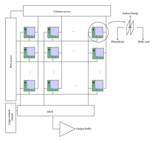
Figure 1 depicts the architecture of the ROIC, whose readout timing operates on pixel level. Snapshot mode is employed. Each pixel corresponds to each readout unit cell, which are connected electrically through indium bump [6]. All the pixels are exposed to radiation simultaneously and transfer the generated photocurrent to the corresponding readout unit cells. Utilizing the architecture provides the capability of expanding integration time, which can adapt to the situation of low intensity radiation [7]. After an integration period ends, with the control of digital logical signals, the integration voltage maintained in each readout unit cell is transmitted serially through a multiplexer and then delivered outside the ROIC through a buffer.
3. Design of the Readout Unit Cell
The structure of the proposed readout unit cell is shown in Figure 2, constituted by two parts, an integrator and a CDS. The integrator adopts the CTIA structure, which provides nearly 100% injection efficiency and linearity. Meanwhile the CDS is composed of three OPs, A2, A3, and A4, connected as buffers, two sampling capacitors, and four complementary switches, S1, S2, S3, and S4. From those A2 and A3 act to isolate switching operations between the former and latter circuit part.
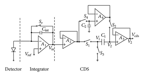
Herein the structure we proposed is compared with four different ROIC unit cells in [8–11]. The added CDS part provides the capability of suppressing low frequency noise from reset operation and photocurrent for the proposed ROIC one which in aspect of noise performance surpasses those referred to in [8–10] without CDS circuits. The linearity of the BDI structure in [11] can reach 99% which is high enough for the type of structure while for the CTIA type like the one we proposed and these in [8–10] it is easy to achieve more than 99.5% linearity; besides, the power dissipation of the two types makes no difference if the static power of the OP involved is the same. Thus how to choose the most suitable OP and optimize the power dissipation of the OPs involved is another crucial problem.
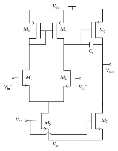
Several types of structure of OP are able to be used for the proposed unit cell, such as cascade OP, folded cascade OP, two-stage OP, and gain boost OP. Table 1 gives the comparison among them [12]. From Table 1 we see that, except for the speed disadvantage, the two-stage OP is the best choice, as shown in Figure 3, which just maintains medium power obtaining high gain which can guarantee low static error. On account of the application of the proposed ROIC unit for infrared image acquisition, the clock operations are not in a high frequency, so the speed of the OPs is easy to achieve in either of the OP types.
| Gain | Output range | Speed | Power | Noise | |
|---|---|---|---|---|---|
| Cascade OP | Medium | Medium | High | Low | Low |
| Folded cascade OP | Medium | Medium | High | Medium | Medium |
| Two-stage OP | High | High | Low | Medium | Low |
| Gain boost OP | High | Medium | Medium | High | Medium |
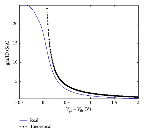
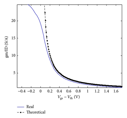
It is worth noting that the behavioural model of MOSFETs in subthreshold region is not accurate enough when the process of ICs goes into deep submicron, like 0.18 μm. To do the calculation precisely, all the parameters adopted should be those obtained through simulations. Figure 4 shows the qualitative illustration of the real gm-to-channel current ratio compared with the theoretical one, (a) for NMOS and (b) for PMOS, from which it can be seen that although the ratio does not increase as fast as the theoretical curve expects when the Vgs − Vth goes down, it is much larger in the subthreshold region than that in the saturation region. That is what we desire to improve efficiency of utilizing current.
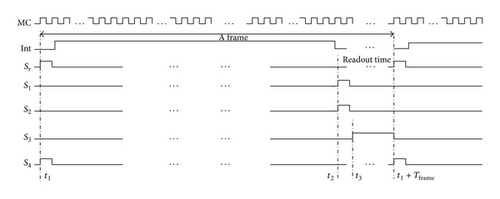
The output node “Vcds” should be equal to “V2” under ideal condition, thus giving the net integration voltage and subtracting the charge injection error brought by the reset process of integrator. However the transmission of signal will be influenced by noise, which is analyzed in the next section in detail.
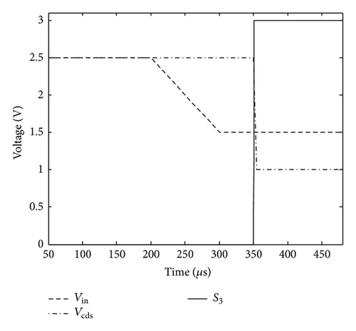
The transient response of the readout unit cell is depicted in Figure 6. We can see that the reset voltage equal to the reference voltage is 2.5 V and the “Vin” node becomes 1.5 V from 2.5 V through integration. At “t3” S3 turns on, the “V1” node connects to ground, and “V2” sets to 1 V, which drives the output voltage to 1 V, the net integration voltage. Besides, the static power dissipation of the proposed readout unit cell reaches 2.8 μW with 700 nW per OP.
4. Noise Model Based on Transfer Function
4.1. The Integrator Part
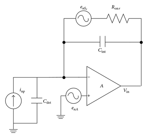
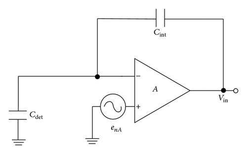
The noise model of the integrator part is shown in Figure 7. There are three noise sources: photocurrent noise caused by photoelectric effect which cannot be avoided [14], the noise caused by the reset process of switch Sr, and the noise of the OP presenting as the input reference noise source.
4.2. CDS Part
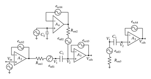
The noise model of the CDS is shown in Figure 9, where all the OPs are connected as unity-gain buffers. Because of the noninverting structure, their output resistance is reduced by A0 times which can be ignored based on the Thevenin equivalent.
5. Noise Computing
5.1. Noise Computing Based on Transfer Function
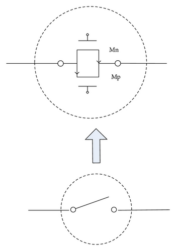
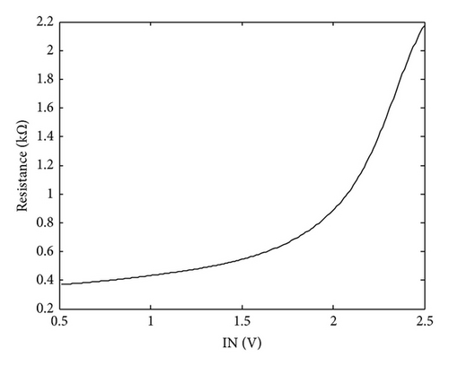
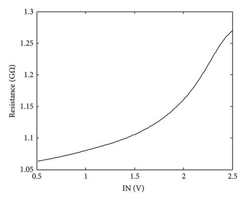
The switches in the proposed ROIC are implemented as CMOS switches, individual of which consists of a P type MOSFET, Mp, and an N type MOSFET, Mn, as shown in Figure 11. The W/L of both of the two MOSFETs are set to be 0.3 μm/2.35 μm. The simulation curve of resistance of the CMOS switch is shown in Figure 12, where the input signal spans from 0.5 V to 2.5 V. Figures 12(a) and 12(b) present the value of maximum on-resistance 2.2 kΩ and the value of minimum off-resistance 1 GΩ.
The parameters used for the calculation of noise are summarized in Table 2, where we assume that all the OPs have the same parameters and so do the switches.
| Ron (on-resistance of switch) | 2.2 kΩ |
| Roff (off-resistance of switch) | 1 GΩ |
| K1e (thermal noise parameter of OP) | 4 × 10⁻¹⁷ V2/Hz |
| K2e (1/f noise parameter of OP) | 4 × 10⁻¹² V2/Hz |
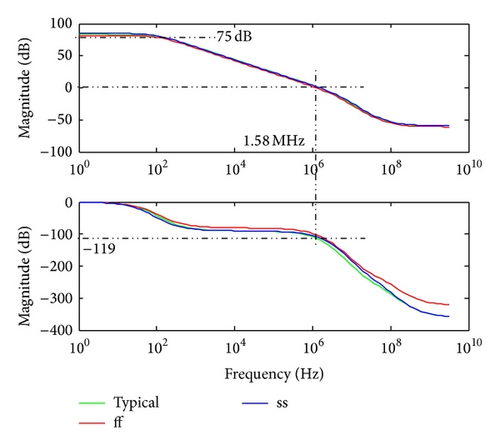
| GBW (gain bandwidth product of OP) | 1.58 MHz |
| A0 (low frequency gain of OP) | 75 dB |
For the application of high resolution, the area of a single pixel is restricted, leading to the limited layout area for the readout unit cell. With respect to the fact that capacitors consume the largest area resource, therefore, with the guarantee of sufficient layout area for the MOSFETs, more layout areas should be distributed to the three capacitors in the unit cell. Through calculations, effect on the output noise due to C2 can be neglected, which should be designed small to save up layout area to allow larger Cint and C1. With the limitation of 30 μm × 30 μm layout area, the maximum of the sum of the two capacitors is 2 pF.
The contribution of each noise source to the output noise is calculated using the transfer functions in Section 3, which is shown in Figure 13, where Tint is set as 100 μs. Figure 13(a) depicts the dependence of the output noise, integrator noise, and CDS noise on the Cint. The diagram reveals an opposite variation trend. The integrator noise is an increasing function and the CDS noise is a decreasing function, which results from the limitation of the sum of capacitors. Cint increase leads to C1 decrease inevitably, causing enlargement of the bandwidth of transfer functions of noise sources in CDS, which weakens the ability of low pass filtering. Figure 13(b) gives the curves of thermal noise, 1/f noise, and reset noise with the change of Cint. We can see that 1/f noise and reset noise increase with Cint increase while an optimal point appears for the thermal noise which is the majority, at 0.66 pF. When the Cint is smaller than 0.26 pF, the reset noise is smaller than 1/f noise. The output noise reaches the minimum at 74.1 μV when the Cint is 0.74 pF and C1 is 1.26 pF.
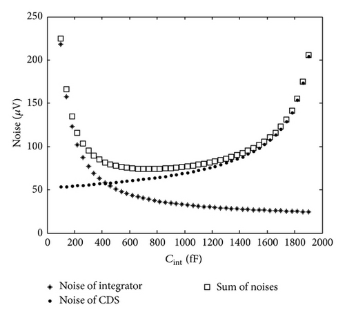
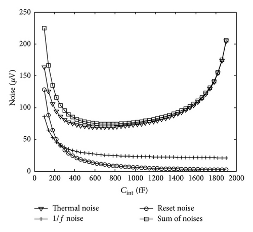
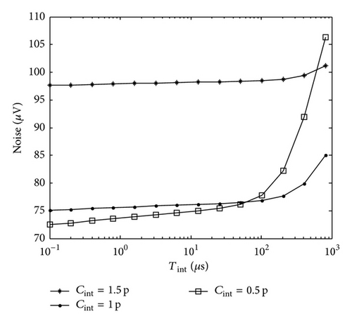
Figure 14 shows the output noise as a function of Tint with three different Cint. It can be seen that the output noise increases when Tint increases, despite different Cint. This is mainly because the increasing of Tint results in increasing of interval of correlated double sampling, which weakens the capability of suppressing 1/f noise and reset noise. From the figure we also get that, with smaller Cint, the increase speed of output noise is faster.
5.2. Noise Calculation Based on Verilog-A
The transient analysis of the proposed readout unit cell is carried out in the section. HSPICE provides the possibility to simulate circuit noise in AC response by computing the PSD but cannot give the waveform of noise in transient response directly, whereas we carried out an approach to model time domain noise source using Verilog-A, which is described in detail in [13, 17] with both thermal and 1/f noise source modelling.
The averaged RMS of the output noise obtained by Verilog-A are presented in Tables 3 and 4 to compare with those that were calculated through transfer functions specified in Section 3, where the unit of noise is μV. In Table 3, Tint is assumed to be 100 μs and Cint is 0.74 pF in Table 4. With different Cint and Tint, the two sets of results are in good agreement, the difference between which is lower than 6%, therefore proving the feasibility of the method of transfer function noise analysis.
| Cint | 100 fF | 460 fF | 820 fF | 1.18 pF | 1.54 pF | 1.9 fF |
|---|---|---|---|---|---|---|
| Theoretical results | 224.7 | 79.5 | 74.4 | 81.5 | 101.9 | 129.2 |
| Verilog-A results | 212.1 | 81.9 | 77.0 | 79.8 | 108.2 | 123.8 |
| Tint | 200 ns | 800 ns | 3.2 us | 12.8 us | 51.2 us | 204.8 us |
|---|---|---|---|---|---|---|
| Theoretical results | 71.5 | 72.0 | 72.5 | 72.9 | 73.5 | 75.9 |
| Verilog-A results | 74.6 | 74.4 | 69.9 | 75.6 | 72.8 | 74.4 |
6. Conclusion
To adapt the application of imaging for large format and high resolution, a new readout cell with low power and small layout area is proposed, consisting of an integrator and a new type of CDS, both of which are switched capacitor circuits where all the MOSFETs are optimized in subthreshold region. The integrator adopts CTIA structure and the CDS is comprised of four switches, three Ops, and two capacitors. The noise model is built using transfer function in Section 3 and a method of presenting the transfer process of noise in the form of matrix is given, through which we can describe the contribution of each noise source to the whole output noise distinctly. In Section 4, noise analysis of the proposed readout cell is carried out by the transfer function method and transient analysis utilizing Verilog-A, respectively. The results showing good agreement verify the feasibility of the method presented through matrix. Under the limitation of layout area less than 30 μm × 30 μm, the integrator noise is an increasing function of Cint and the CDS noise is a decreasing function. With respect to the types of noise, 1/f noise and reset noise increase with Cint increase while an optimal point appears for the thermal noise which is the majority. The integration capacitor should be selected as 0.74 pF to achieve an optimal noise performance, the whole output noise reaching the minimum value at 74.1 μV.
Conflict of Interests
The authors declare that there is no conflict of interests regarding the publication of this paper.
Acknowledgment
The authors thank Key Laboratory of Opto-Electronic Information Processing for the continuous supporting of the research on noise of readout integrated circuits.


