Synthesis of ZnO Nanowires and Their Photovoltaic Application: ZnO Nanowires/AgGaSe2 Thin Film Core-Shell Solar Cell
Abstract
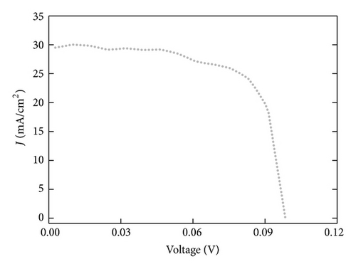
In this investigation, hydrothermal technique was employed for the synthesis of well-aligned dense arrays of ZnO nanowires (NWs) on a wide range of substrates including silicon, soda-lime glass (SLG), indium tin oxide, and polyethylene terephthalate (PET). Results showed that ZnO NWs can be successfully grown on any substrate that can withstand the growth temperature (~90°C) and precursor solution chemicals. Results also revealed that there was a strong impact of growth time and ZnO seed layer deposition route on the orientation, density, diameter, and uniformity of the synthesized nanowires. A core-shell n-ZnO NWs/p-AgGaSe2 (AGS) thin film solar cell was fabricated as a device application of synthesized ZnO nanowires by decoration of nanowires with ~700 nm thick sputtering deposited AGS thin film layer, which demonstrated an energy conversion efficiency of 1.74% under 100 mW/cm2 of simulated solar illumination.
1. Introduction
In recent years, there has been an increasing amount of literature on both one-dimensional nanostructures synthesis and employment of a wide range of thin film semiconductor materials for the realization of high-efficiency, low-cost solar cells. However, there are a quite few research studies on combining these efforts. In this regard, employing one-dimensional (1D) nanostructures such as nanowires (NWs), nanorods (NRs), and nanotubes (NTs) to construct three-dimensional (3D) device architectures is a very promising approach for the realization of next-generation high-efficiency solar cells at lower cost [1, 2].
In the past two decades, to improve the performance of solar cells, 3D photovoltaic device architectures including axial architecture, radial architecture (core-shell), and nanostructures embedded in thin film models have been studied extensively with different material combinations [2]. In particular, core-shell architecture offers significant advantages over its planer counterparts due to its unique properties, such as light trapping, efficient charge collection, quantum confinement, and decoupling the photon absorption and carrier collection in an effective way. Currently, silicon (Si), titanium dioxide (TiO2), and zinc oxide (ZnO) are the most commonly employed semiconductor materials for the construction of core-shell solar cells as the core component. There are many potential reasons to choose these materials such as their abundance in the earth crust, nontoxic nature, convenient bandgap nature/energy value, stability, and outstanding chemical/physical and optical properties [3]. In core-shell structure, the shell component plays a crucial role in determining the performance of the designed device [4–6]. As a shell component, chalcopyrite semiconductors (CuInSe2, Cu(In, Ga)(S, Se)2, and Ag(In, Ga)(S, Se)2) are regarded as promising candidates due to their convenient bandgap nature and energy value, which exactly matches the most abundant part of solar spectrum reaching the surface of the earth [7, 8]. Therefore, the proper bandgap nature/energy value of these materials suggests that more than 90% of the incident light can be absorbed in a few micrometers of the material [9]. Chalcopyrites along with CdTe are regarded as the most promising semiconductors alternatives to Si and are at the heart of today’s thin film based solar cells [10].
In the present investigation, we have constructed 3D core-shell solar cell by employing a sputtered AgGaSe2 (AGS) thin film as shell component due to its high absorption coefficient (~105 cm−1) and convenient bandgap nature/energy (direct bandgap with ~1.8 eV). It is a well-known fact that AGS semiconductors can also be used for many other applications including frequency doubling (CO2 laser output) and photodetectors [11–15]. For the core component of the fabricated solar cell, ZnO material was preferred, a semiconductor with a large bandgap (3.37 eV) and exciton binding energy (60 meV) at room temperature, due to its many outstanding properties such as the piezoelectricity, near band emission, and transparent conductivity. ZnO has been widely used for many optoelectronic devices so far, including solar cells, light-emitting diodes (LEDs), and gas sensing [3, 16–18].
A wide range of fabrication techniques have been reported in literature so far for the synthesis of 1D nanostructures, which can be classified into different routes: (i) vapor and (ii) solution based techniques [19–21]. Of several solution based approaches, hydrothermal technique is of a special interest due to its many advantages such as low growth temperature, ease of controllable doping, reliable and contamination-free growth, tunable physical parameters, allowing mass production, and no requirement of vacuum and expensive equipment [22]. Based on these considerations, therefore, in the present study, ZnO NWs were synthesized using hydrothermal technique.
The object of this study is to synthesize ZnO nanowires (NWs) by hydrothermal technique and then incorporate them into AgGaSe2 chalcopyrite thin film to fabricate a core-shell structured solar cell. As n-ZnO NW/p-AgGaSe2 core-shell type heterojunctions have not been studied so far, it is going to be the first study reporting solar cell parameters of the device associated with these material combinations.
2. Experimental
ZnO NWs were grown onto different substrates including soda-lime glass (SLG) precoated with indium thin oxide (ITO), SLG, PET (polyethylene terephthalate), and n-Si wafer substrates ((100) orientation and 1–10 (Ω·cm) resistivity) using hydrothermal growth technique. For the synthesis of ZnO NWs, ~30 nm thick ZnO seed layers were deposited onto the aforementioned substrates by using both sputtering and sol-gel techniques. Sputter-deposited seed layers were deposited using a radiofrequency (RF) magnetron system, the employed power of which was 150 W under 5 × 10⁻³ Torr in Ar atmosphere. For the fabrication of ZnO seed layers by sol-gel route, a ZnO precursor solution was prepared by dissolving zinc acetate dihydrate [ZnAc:Zn(COOCH3)2·2H2O] in 2-propanol and diethanolamine (DEA, C4H11NO2), assigned as solute, solvent, and chelating agent, respectively. The molar ratios of DEA/ZnAc and H2O/ZnAc were chosen as 1 and 1/2, respectively, to prepare a solution with 0.4 M concentration, details of which have been given elsewhere [17, 23]. The precursor solution was stirred at 70°C for 1 h to get a clear and homogenous solution. After that, ZnO seed layers were deposited on precleaned SLG substrates by spin coating at one step with spinning speed of 5000 revolutions per minute (rpm) for 1 min. The spin coating process was based on a single stage coating process to obtain ~30 nm thick ZnO seed layer. Spin-coated seed layers were first preheated at 300°C on hot plate for 10 min and then annealed at 550°C for 1 h in ambient air for the complete crystallization of seed layer and evaporation of the remained organics in the thin film structure. Following the deposition of the ZnO seed layer, the substrates were subjected to a solution based on equimolar 25 mM (Zn(NO3)2)·6H2O (zinc nitrate hexahydrate, Sigma-Aldrich) and HMTA (hexamethylenetetramine, Sigma-Aldrich) as precursors in deionized (DI) water (with 18 MΩ·cm resistivity). During the synthesis of ZnO nanowires, the solution temperature and the growth time were set to 90°C and 1.5–3 hours, respectively [16].
For the fabrication of n-ZnO NWs/p-AgGaSe2 core-shell solar cell, ZnO NWs grown on SLG substrate (precoated with ITO) were decorated with AgGaSe2 (AGS) thin films. For the deposition of AGS thin films, a three-source sputtering system (Vaksis) was preferred. Four-inch Ag and GaSe sputtering targets (at a tilt angle of 30°) were used as sources for the sequential deposition of Ag and GaSe thin film layers. For the plasma generation in the chamber, argon gas with 99.99% purity was employed, which was set to 6 sccm during the film deposition. The distance between targets and the substrate during the deposition cycle was around 25 cm. To enhance the uniformity of AGS thin films, the substrate was rotated on a heated plate during deposition process. As it is semi-insulating material, for the deposition of GaSe thin film RF sputtering was used with power of 75 W under 5 × 10⁻³ Torr Ar gas pressure. The deposition of Ag thin film layers was carried out by DC magnetron sputtering with a 20 W power in a 5 × 10⁻³ Torr Ar gas pressure atmosphere. The deposition rates for the sequentially deposited Ag and GaSe layers were chosen as 1 Å/s and 2 Å/s, respectively. Prior to decoration of ZnO NWs with AGS, to optimize the quality of AGS thin films, single layers of Ag and GaSe were sequentially deposited on SLG substrates to form GaSe/Ag/GaSe/Ag/GaSe/Ag/GaSe/Ag/GaSe multilayers. During the optimization cycle the substrate temperature remained constant at 150°C and the thickness of Ag and GaSe layers was set to 20 nm and 125 nm, respectively. Both deposition rate and thickness of each layer were simultaneously monitored with integrated oscillatory quartz (Inficon XTM/2). Following the sequential deposition of Ag and GaSe layers, they were annealed in vacuum at temperature of 275°C for 30 min to trigger the interdiffusion of multilayers. In addition, to investigate the effect of annealing on physical properties of deposited AgGaSe2 thin films, the postannealing in the temperature range of 300–550°C was employed, which was carried out on a hot plate under N2 gas flow for 30 min. After optimization stages of thin film, a ~700 nm thick AGS layer was deposited onto the synthesized ZnO NWs for the realization of SLG/ITO/n-ZnO NWs/p-AgGaSe2 core-shell solar cell. For the top and bottom contacts of the device, thermally evaporated indium dot contacts (using a dot-patterned copper mask) and SLG precoated with ITO were employed, respectively.
To determine the structural, electrical, and optical properties of deposited AGS thin films several characterization techniques have been applied. The crystal structure and orientation, existing material phases, and the size of the grains were determined by means of X-ray diffraction (XRD) using a Scintag XDS2000 powder X-ray diffractometer with CuKα radiation source. The optical properties were investigated by performing transmission measurements in the wavelength range of 300–1100 nm using an Ocean Optics UV-VIS spectrometer. Electrical measurements were carried out using a four-point van der Pauw method. Ohmic contacts on chalcopyrite thin films (AGS) were achieved by thermal evaporation of high pure In using a convenient copper mask. For the electrical characterization of AGS thin films, following the confirmation of ohmic nature of contacts, temperature dependent conductivity and photoconductivity measurements were carried out in temperature range of 100–430 K in a Janis cryostat equipped with Keithley’s 220 current source, Keithley’s 619 electrometer, Keithley’s 2400 digital SourceMeter and a Lake shore 331 temperature controller. The surface morphology, composition, and thickness of deposited thin films as well as the morphology of ZnO NWs were determined by a Hitachi S-4100 FE scanning electron microscopy (SEM) equipped with EDXA. The current-voltage (I-V) characteristic of fabricated solar cell was measured at room temperature (300 K) using a LabVIEW controlled Keithley’s 2400 SourceMeter. Finally, testing of fabricated solar cells was performed in Oriel 1000 W solar cell simulator setup (under AM 1.5 conditions), which was controlled with Newport I-V test software.
3. Results and Discussion
Figure 1 shows typical scanning electron microscope (SEM) image of ZnO nanowires (NWs) grown on different substrates including silicon (Si), soda-lime glass (SLG), indium tin oxide (ITO) precoated SLG, and polyethylene terephthalate (PET) by using hydrothermal technique. ZnO NWs were grown on the aforementioned substrates precoated with ~30 nm thick ZnO seed layer deposited by RF sputtering. Growth time and temperature were chosen as 3 h and 90°C, respectively.
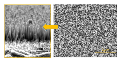
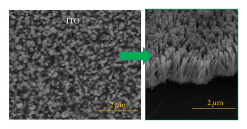
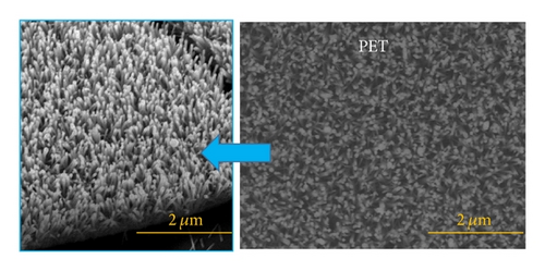
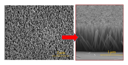
From the images presented in Figure 1, it is apparent that ZnO NWs are 1.2–1.3 μm long and 65–95 nm in diameter, which are nearly uniformly distributed over the surface of the substrates. In addition, it can be seen from the images that highly dense and vertically well-oriented ZnO NWs can be grown on any substrates as long as they can withstand growth temperature (~90°C) and chemical used in the precursor solution required for growth of NWs by hydrothermal approach. In particular, the growth of ZnO NWs on a flexible substrate such as PET is very important since it allows the realization of flexible optoelectronic devices including UV photodetectors, solar cells, and light emitting diodes (LEDs).
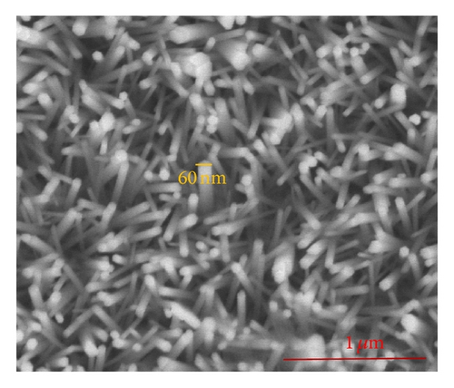
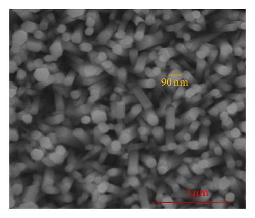
In order to reveal the effect of growth time on diameter of ZnO NWs, grown on sputter-deposited ZnO seed layer with thickness of ~30 nm onto SLG substrates, growth was carried out for 1.5 h and 3 h time duration by keeping the other growth parameters constant. As can be seen from SEM images illustrated in Figure 2, there is a significant difference between the diameters of grown ZnO NWs for these growth time durations, which are ~60 nm and ~90 nm for 1.5 h and 3 h, respectively. The present findings on the relation between growth time and nanowire diameter seem to be consistent with other findings of a great deal of the previous works focused on this correlation. The observed increase in diameter with increasing growth time is generally attributed to the coalescence of poor-oriented longer NWs. It is possible, therefore, that, by using the revealed correlation between these two parameters, the aspect ratio of ZnO NWs can be adjusted for specific device applications, such as light scattering, guiding, and trapping to enhance the absorption of incident light for photovoltaic applications.
In addition to the effect of growth time, the effect of seed layer deposition route on the morphology of ZnO NWs has been determined by comparing the quality of NWs grown on ZnO seed layers deposited by sol-gel and sputtering techniques, SEM images of which are presented in Figure 3. During the NW growth stage all the growth parameters including temperature, precursor concentration, and orientation of substrate with respect to the wall of beaker and growth time except seed layer deposition approach were kept constant to reveal the effect of this parameter. As can be seen in Figure 3, there is a significant difference between the quality of NWs grown on seed layers deposited by different routes in terms of density, orientation, and uniformity of synthesized NWs. The obtained results suggest that seed layer deposition route has a strong impact on NW quality and the best quality comes with NWs grown on sputter-deposited ZnO seed layer.
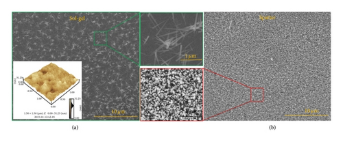
In other words, it was observed that well-oriented, homogenously distributed dense arrays of ZnO NWs were synthesized on sputter-deposited ZnO seed layer, which was not the case for the NWs grown on sol-gel deposited one. To understand the origin of this difference, the atomic force microscope (AFM) measurement was conducted for the ZnO seed layer deposited by sol-gel, image of which is given as inset in Figure 3(a). It is clear from this image that the surface of the deposited seed layer is not uniform and consisted of well-like features that randomly distributed over the surface. As expected, it is not possible to deposit very uniform continuous ZnO thin film layers by sol-gel as opposed to sputtered layers, which promotes the formation of these features. Among the plausible explanation for the observed low quality of ZnO NWs grown on sol-gel deposited seed layer, in terms of orientation, density, and uniformity, we can suggest that it is these well-like features which trigger the formation of poor-oriented low quality NWs. In other words, these randomly distributed features may function as seeding centers that promote the formation of ZnO NW nucleations, from which NWs derive. It is, therefore, expected that the shape and density of these features will be the two important factors that will assign the quality of synthesized ZnO NWs.
To investigate the stoichiometry of deposited AgGaSe2 thin films, energy dispersive X-ray analysis (EDXA) measurements were performed at 20 keV for as-grown sample. The EDXA pattern and atomic percentage of constituent elements are given in Figure 4. As expected, all constitute elements appeared in the spectrum at specific energy values (Figure 4(b)). Based on the measured values of atomic percentage of elements, it is possible to claim that a nearly stoichiometric AgGaSe2 thin film (inside the interval of experimental error limit (1-2%)) is successfully obtained.
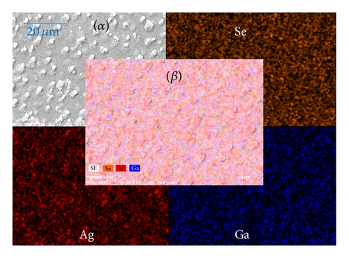
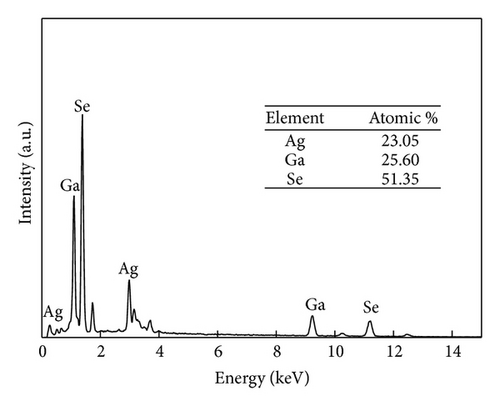
Beside the EDAX pattern, as shown in Figure 4(a), we have obtained elemental mapping for constitute elements for as-grown thin film to determine the distribution of elements in the sequential layers of deposited AgGaSe2 thin film. It is clear from the map that Se and Ag elements cover the majority part of surface, while Ga is just beneath them, which implies the existence of uncompleted reaction for the construction of an ordered AgGaSe2 structure, possibly due to insufficient heat energy supplied during deposition process (150°C).
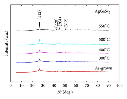
Figure 5 shows the X-ray diffraction pattern recorded for as-grown film and AgGaSe2 thin film annealed in the temperature range of 300–550°C. As can be seen from the figure, the as-grown film is polycrystalline and consisted of single phase AgGaSe2 having chalcopyrite structure with lattice parameters of a = b = 5.993 Å and c = 10.884 Å [24]. Following the postannealing between 300 and 550°C, it was observed that the intensity of all peaks which appeared in XRD pattern increases gradually with increase in annealing temperature, which closely related with the improvement in crystallinity. The improvement of crystallinity can be attributed to the elimination of imperfections in structure following the postannealing process at high temperatures. In our previous studies, although several attempts have been made to deposit single phase AGS at low substrate or annealing temperatures, we could not achieve it due to either appearance of secondary phases such as Ag or the requirement of deposition of this material on substrates that can withstand high annealing temperature (>550°C). But here with this study we report the achievement of producing a single phase AGS at quite low substrate temperature (150°C). Obtaining a thin film in a single phase without any secondary phases is essential for a precise control on optoelectronic devices such as solar cells.
The optical transmittance of deposited and AgGaSe2 thin films has been determined in the wavelength range of 325–1100 nm. The obtained spectra for as-grown film and film annealed between 400 and 550°C are presented in Figure 6(a). It can be seen from the transmission spectra that the postannealing process has a remarkable effect on transmittance of AGS thin films.
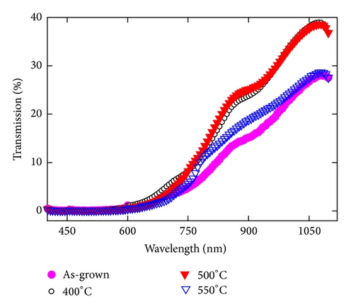
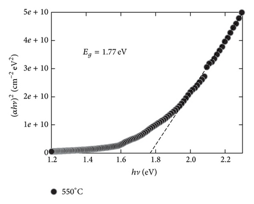
That is, it was observed that there is a systematic increase in transparency with increasing annealing temperature, except for the annealing temperature of 550°C. The observed increase in transparency may be due to the structural modifications deduced from XRD study in which an improvement in crystallinity was deduced after postannealing process. In other words, postannealing process may end up with reducing defects in polycrystalline structure by which a better crystallinity and homogeneity provided. This may subsequently result in less scattering of light and enhancement in transparency. The optic bandgap (Eg) and absorption coefficient (α) of the deposited films were calculated through transmission spectra presented in Figure 6(a). The relation between absorption coefficient and photon energy (hν) for the film annealed at 550°C is shown in Figure 6(b). From this relation, the optic bandgap can be determined through the extrapolation of its linear portion of plot to zero absorption coefficient. The bandgap was found to be around 1.77 eV, which is in a close agreement with reported values in literature [12].
The temperature dependent conductivity measurements were carried out in the temperature range of 100–430 K for as-grown film and films annealed between 400 and 550°C. The variation of conductivity as a function of temperature is shown in Figure 7(a).
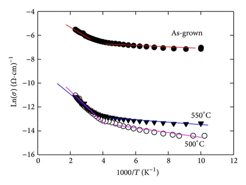
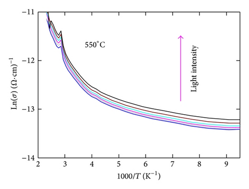
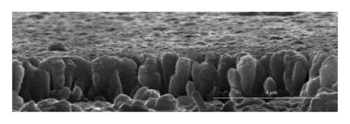
Figure 8(a) Shows SEM image of the structure of a fully fabricated n-ZnO NWs/p-AgGaSe2 core-shell solar cell. It is apparent from the image that ZnO NWs are decorated with sputtered AgGaSe2 layer for the realization of p-n heterojunction solar cell. It is also clear that the AGS layer at the top part of ZnO NWs is thicker than that at the bottom part, which can be attributed to the limitation of our technique, sputtering, for the decoration of AGS layer [26]. In other words, ZnO NWs are not conformally coated with AGS layer and are thicker than desired. Therefore, ZnO NWs in the completed solar cell structure are connected by the p-AGS canopy layer (a continuous film), resulting in a planer surface of a hybrid thin film nanowire structured device. For a core-shell structured solar cell, although it is reasonable to expect enhanced carrier collection efficiency, it is not the case for optical properties, which are almost similar to thin film or wafer-based solar cell architecture owing to its planer top surface [27]. As the fabricated device is the first prototype, there are many issues we must address. The surface morphology is among them. Our ongoing work has focused on adjusting the shell layer’s thickness for the realization of conformally coated ZnO NWs, which are desired for the more incident light absorption through light trapping and scattering.
4. Conclusions
Dense arrays of ZnO nanowires (NWs) were successfully synthesized on different substrates such as silicon, soda-lime glass (SLG), indium tin oxide (ITO), and polyethylene terephthalate (PET) by employing hydrothermal technique. In particular, the growth of ZnO NWs on a flexible substrate such as PET is very important since it would allow the realization of flexible optoelectronic devices including photodetectors, solar cells, and light emitting diodes. During the nanowire growth cycle, it was found that there was an important correlation between growth time and the diameter of NWs; in other words, there was an increase in diameter with increasing growth time, which was attributed to the coalescence of poor-aligned NWs at longer times. In addition to this, results revealed that there was a strong impact of the deposition routes of ZnO seed layer, which were sol-gel and sputtering, on quality of synthesized ZnO NWs in terms of orientation with respect to the normal of the substrate, diameter, homogeneity in length, uniformity, and density of nanowires.
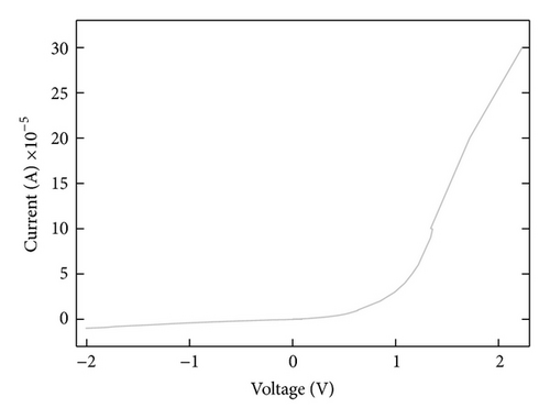
As an application of synthesized ZnO NWs, a core-shell type solar cell based on n-ZnO NWs/p-AgGaSe2 (AGS) materials combination was fabricated. Prior to realization of the device structure, AGS thin films were deposited on SLG substrates via sputtering technique and then structural, electrical, and optical properties were investigated in detail. Once the best quality AGS thin film was obtained, ZnO NWs were decorated with it for the construction of a core-shell structured solar cell. From the measurement under 100 mW/cm2 of simulated solar illumination, the open-circuit voltage, short circuit current density, fill factor, and energy conversion efficiency were found to be 0.098 V, 29.40 mA/cm2, 60.25%, and 1.74% respectively, which could be taken as encouraging results for next generation nanowire based solar cells and will serve as a base for future studies.
Conflict of Interests
The authors declare that there is no conflict of interests regarding the publication of this paper.
Acknowledgment
This work was supported by Turkish Scientific and Research Council (TUBITAK) under Grant no 114F251.


