All Pass Network Based MSO Using OTRA
Abstract
This paper presents multiphase sinusoidal oscillators (MSOs) using operational transresistance amplifier (OTRA) based all pass networks. Both even and odd phase oscillations of equal amplitudes which are equally spaced in phase can be produced using single all pass section per phase. The proposed MSOs provide voltage output and can readily be used for driving voltage input circuits without increasing component count. The effect of nonideality of OTRA on the circuit performance is also analysed. The functionality of the proposed circuit is verified through PSPICE simulations.
1. Introduction
Multiphase sinusoidal oscillators (MSO) provide multiple outputs of the same frequency, equally spaced in phase, and find extensive application in the field of communications, instrumentation, and power electronics. In communications MSO circuits are used in single-sideband generators, phase modulators, and quadrature mixers [1]. Selective voltmeters and vector generator are common applications of MSOs in the field of instrumentation [2]. In power electronics three-phase MSOs are frequently utilized in PWM converters [3] and inverters [4].
A large number of MSO realizations using various analog building blocks (ABB) [2, 5–25] are available in literature. These MSOs are based on a basic design philosophy of forming closed loop using n (n ≥ 3) cascaded phase shifting networks thereby producing n equally spaced phases. For phase shifting either first-order low pass networks (LPNs) [5–7, 9–21, 24, 25] or first-order all pass networks (APNs) [2, 8, 22, 23] are used. These reported structures provide either voltage [5–16] or current [2, 17–24] outputs.
The MSOs of [5–8] are realized using operational amplifiers (op-amps). However due to constant gain-bandwidth product and lower slew rate of the op-amps, their high frequency operations are limited. Additionally the active R implementations of [5, 6] lack tunability as these structures make use of the op-amp parasitic capacitance. The current feedback operational amplifier (CFOA) based MSO structure [9] is capable of producing high frequencies but requires an accessible compensation terminal of a CFOA. The MSOs of [10, 11] are OTA based electronically tunable structures; however, they provide voltage output at high impedance making a buffer necessary to drive the voltage input circuits. In addition, for both the structures the output voltage is temperature sensitive too. The MSO configurations presented in [12–15] are CC based designs and provide voltage output at high impedance. Further the MSO of [14], being active R structure, lacks tunability. Three topologies of OTRA based MSOs are proposed in [16] and are designed using LPNs. The structures proposed in [2, 17–25] provide current outputs which need to be converted back to voltage for circuits requiring voltage inputs, which would considerably increase the component count. A detailed comparison of these structures is given in Table 1 which suggests that OTRA based MSO is the most suitable choice for voltage output.
| Reference | ABB | Phase shift network | Output | Output impedance | Tunability |
|---|---|---|---|---|---|
| [2] | CCCDTA | APN | Current | High | Yes |
| [5] | Op-amp | LPN | Voltage | Low | No |
| [6] | Op-amp | LPN | Voltage | Low | No |
| [7] | Op-amp | LPN | Voltage | Low | Yes |
| [8] | Op-amp | APN | Voltage | Yes | Yes |
| [9] | CFOA | LPN | Voltage | No | Yes |
| [10] | OTA | LPN | Voltage | High | Yes |
| [11] | OTA | LPN | Voltage | High | Yes |
| [12] | CCII | LPN | Voltage | High | Yes |
| [13] | CCII | LPN | Voltage | High | Yes |
| [14] | CCII | LPN | Voltage | High | No |
| [15] | CCII | LPN | Voltage | High | Yes |
| [16] | OTRA | LPN | Voltage | Low | Yes |
| [17] | Current follower | LPN | Current | High | Yes |
| [18] | CCII | LPN | Current | High | Yes |
| [19] | CCII | LPN | Current | High | Yes |
| [20] | CCII | LPN | Current | High | Yes |
| [21] | CDTA | LPN | Current | High | Yes |
| [22] | CDTA | APN | Current | High | Yes |
| [23] | CDTA | APN | Current | High | Yes |
| [24] | CC | LPN | Current | High | Yes |
| [25] | CFTA | LPN | Current | High | Yes |
| Proposed work | OTRA | APN | Voltage | Low | Yes |
In this paper authors aim at presenting OTRA based MSO, designed using APNs. The proposed circuit utilizes n (n ≥ 3) APNs to produce n phase oscillations of equal amplitudes with a phase difference of (360/n)°. The APN can produce a phase shift up to 180° as against a maximum of 90° produced by LPN. As a result the APN based scheme can be used to implement an even phase system for n = 4 also whereas n = 6 is the minimum for the systems designed using LPNs [8].
2. Circuit Description
In this section the generalized APN based MSO scheme [8] is described first which is followed by the design adaption using OTRA.
2.1. The APN Based MSO Design Scheme
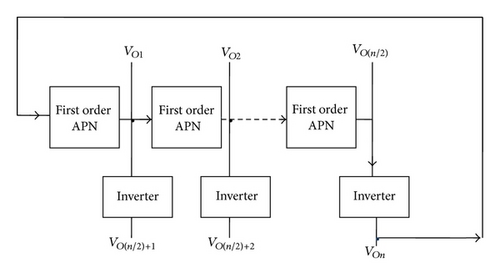
The APN based MSO structure consists of n cascaded first-order APN blocks. The output of the nth stage is fed back to the input of the first stage thus forming a closed loop as shown in Figure 1(a). The output of nth stage is fed back directly for odd phase system whereas for even phase system it is inverted, for sustained oscillations. In case of even phased system the structure can be modified for obtaining n even phased oscillations by replacing n/2 APN with n/2 inverters as shown in Figure 1(b).

2.2. The OTRA Based MSO Implementation
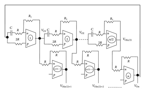
3. Nonideality Analysis
4. Simulation Results
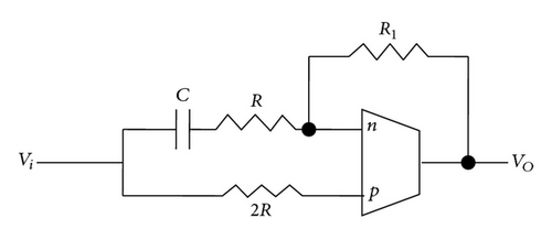
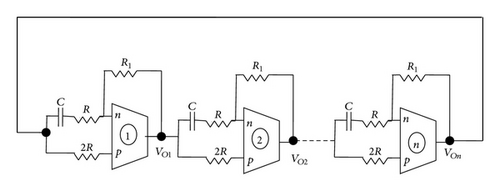
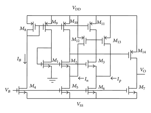
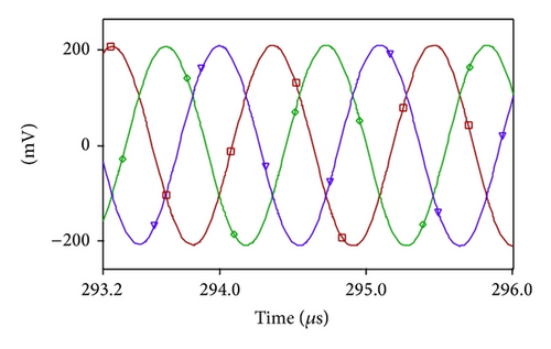
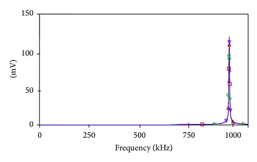
The proposed circuits are simulated using PSPICE to validate the theoretical predictions. The CMOS realization of OTRA presented in [28] and reproduced in Figure 5 is used for simulation. The output of the MSO of Figure 4(a) for n = 3, with component values R = 2.5 KΩ, R1 = 5 KΩ, and C = 0.1 nF, is depicted in Figure 6. The steady state output is shown in Figure 6(a) while the frequency spectrum is depicted in Figure 6(b). The simulated frequency of oscillations is observed to be 1 MHz against the calculated value of 1.1 MHz.
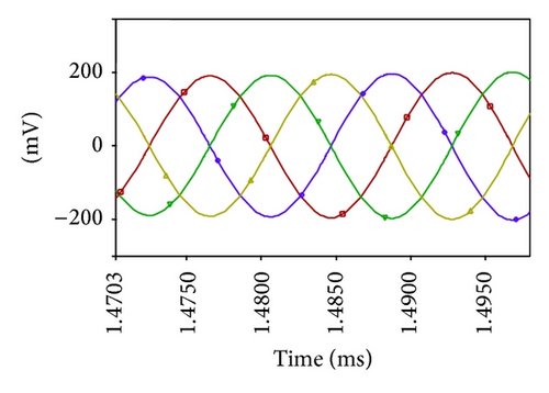
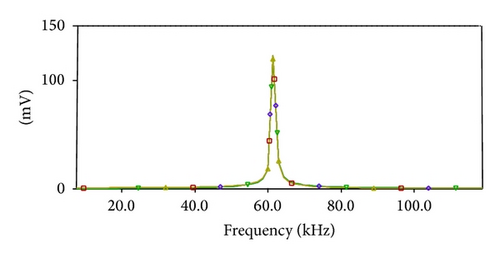
Simulation results for n = 4, with component values R = 2.5 KΩ, R1 = 5 KΩ, and C = 1 nF, are depicted in Figure 7. The simulated frequency is found to be 61.69 KHz while the theoretical calculation yields an FO of 63.69 KHz.
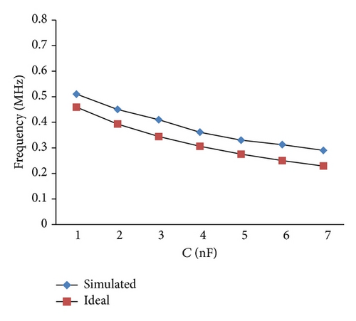
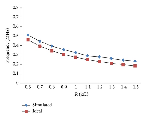
It may be observed from (8) that the FO can be varied either through R or by changing C. Variation of FO with respect to R while keeping C = 1 nF has been depicted in Figure 8(a) whereas tuning with C is shown in Figure 8(b) with R = 0.5 KΩ. It shows that the simulated values closely follow the theoretically calculated values.
5. Conclusion
In this work OTRA based MSO circuits, designed using first-order all pass networks, are presented. The proposed structures produce “n” phase oscillations of equal amplitudes which are equally spaced in phase. These circuits provide voltage output at low impedance and thus can readily be used to drive voltage input circuits without increasing component count. The proposed circuits are very accurate in providing the desired phase shift. The workability of the circuit has been demonstrated through PSPICE simulations.
Conflict of Interests
The authors declare that there is no conflict of interests regarding the publication of this paper.


