The Design of Low Noise Amplifiers in Deep Submicron CMOS Processes: A Convex Optimization Approach
Abstract
With continued process scaling, CMOS has become a viable technology for the design of high-performance low noise amplifiers (LNAs) in the radio frequency (RF) regime. This paper describes the design of RF LNAs using a geometric programming (GP) optimization method. An important challenge for RF LNAs designed at nanometer scale geometries is the excess thermal noise observed in the MOSFETs. An extensive survey of analytical models and experimental results reported in the literature is carried out to quantify the issue of excessive thermal noise for short-channel MOSFETs. Short channel effects such as channel-length modulation and velocity saturation effects are also accounted for in our optimization process. The GP approach is able to efficiently calculate the globally optimum solution. The approximations required to setup the equations and constraints to allow convex optimization are detailed. The method is applied to the design of inductive source degenerated common source amplifiers at the 90 nm and 180 nm technology nodes. The optimization results are validated through comparison with numerical simulations using Agilent’s Advanced Design Systems (ADS) software.
1. Introduction
The low-noise amplifier (LNA) is the critical component in the analog front-end of a radio frequency (RF) receiver. The LNA is responsible for providing sufficient amplification of weak input signals while minimizing the amount of added electronic noise and distortion. As a result, the characteristics of the LNA set the upper limit on the performance of the overall communication system. The optimization of the LNA is a complex task involving tradeoffs that must be made among several competing parameters including noise figure, linearity, and impedance matching [1]. While bipolar technologies have traditionally dominated RF designs due to their superior switching frequency and gain, they are not particularly suited for low power design and are not directly compatible with scaled digital CMOS processes. In the late 1990s, the transit frequency of CMOS devices reached the 40 GHz range, which enabled the design and implementation of RF CMOS circuits that could process signals on the order of 4 GHz [2]. A combination of improved processing technology, suitable MOS circuit architectures, and amenable wireless standards have helped push CMOS technology to the forefront for RF circuit implementations [3–5]. Implementing high quality RF analog circuits on scaled digital processes is a desired goal for a couple of reasons. First, a prime motivation is the increased integration densities and resulting lower costs. Second, it allows the realization of a complete RF transceiver on a systems-on-a-chip (SoC) implementation, which would further improve design flexibility and system optimization [6]. An SoC design with digital, analog, and RF components will pave the way for radio systems that are largely software-controlled digital devices [3]. While the digital components dominate in a software-defined radio (SDR) architecture, the analog front-end including the LNA will remain the critical component that determines the overall system performance.
In the rapidly growing consumer demand for portable wireless devices with long battery life, obtaining sufficient receiver sensitivity while minimizing power dissipation is a major design objective. As process scaling continues to shrink the dimensions of the CMOS transistors, RF circuits will benefit from the improved switching frequencies. However, the main issue will be the reduction in performance due to increased thermal noise from MOSFETs implemented in scaled digital CMOS processes and lower gain and signal swing headroom as voltage supplies are inevitably decreased. With reduction in the analog voltage supplies, an increase in power dissipation is required in order to maintain constant performance [7]. Hence, innovations in circuit topologies and optimization methods will be required to maintain low power and high performance as device scaling continues deep into the nanometer-scale dimensions.
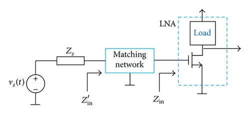
A common design methodology is to determine the minimum noise that can be obtained given constraints on impedance matching and power dissipation. Using classical two-port noise theory, the optimum impedance that must be presented at the source of the LNA in order to achieve the minimum noise figure (NF) can be calculated. An appropriate matching network is inserted between the source and the LNA to help achieve this goal as illustrated in Figure 1. It is well known that maximum power transfer between the source and the amplifier input occurs when the complex conjugate of matches the source impedance Zs [1]. Common-source (CS) amplifiers have been the most popular CMOS LNA circuit topologies due to their good low-noise performance and high gains. However, when using a CS amplifier, the input impedance Zin presented by the MOSFET makes it difficult to optimally match with the external impedance Zs , which is generally resistive in nature [8]. Hence, tradeoffs in terms of noise performance and gain must be made with this architecture.
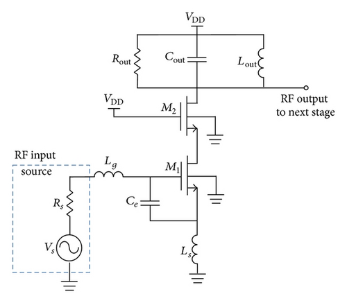
The basic amplifier architecture illustrated in Figure 2 allows the noise figure to be minimized while achieving input matching under power constrained conditions. The addition of inductive source degeneration and an input impedance matching inductive component, denoted by Ls and Lg, respectively, allows improved impedance matching to be obtained over a narrow band of interest. The addition of the capacitance Ce gives the added design flexibility of meeting a given power dissipation and input matching specification while maintaining a very low noise performance [9]. The cascode device M2 provides isolation with the load.
Efficient and accurate optimization techniques for implementing analog integrated circuits are a critical facet of a CAD-based design flow. This is essential when the goal is to minimize the time-to-market for a product, and thus have working designs on first silicon [10]. While the noise analysis of a linear two-port network provides some insight into how to optimize the noise figure (NF) of an amplifier [11], this classical approach does not provide any guidance on the sizing of the devices. Various approaches that incorporate suitable FET device characteristics and noise models into the design process have been developed [12–14]. In order to account for second order effects in devices as scaling occurs, two general optimization strategies can be used: simulation-based and equation-based methods. A simulation-based approach allows more general topologies and circuit parameter variations to be explored. However, there are a couple of drawbacks to this approach. First, as metaheuristic algorithms, such as genetic algorithms and other evolutionary techniques, are often used, this approach is very computationally intensive. This is due to the large number of iterations that require detailed circuit simulations to be executed [15–18]. Second, there is no guarantee that a globally optimum solution is found. On the other hand, equation-based methods attempt to formulate a solution for a more restricted set of parameters and usually for a predetermined circuit topology. Geometric programming methods are able to find a globally optimum solution very efficiently for a well-formulated problem [19]. The trade-off in this case is that certain approximations must be made to ensure that the device equations are in a form suitable for numerical optimization. However, once the system is set-up, a globally optimum design can quickly be found.
In this paper, the focus is on the optimization of a specific topology, the CS CMOS LNA, when short-channel effects such as excess thermal noise must be taken into consideration. As such, we will make use of convex optimization, a form of geometric programming. Geometric programming (GP) has been previously employed to optimize a variety of integrated circuit designs, including both analog and digital circuits [20–25]. For a comprehensive overview and list of GP applications, see [19]. The approach in this paper is to optimize the NF of the CS LNA subject to various constraints such as input circuit quality factor, power consumption, and input impedance matching, similar to [12]. The optimization procedure will allow the globally optimum selection of device parameters. Geometric programming has been used to optimize the design of RF CMOS low-noise amplifiers at the 0.35 μm technology node [26] using the design proposed in [9]. While the work by [26] results in globally optimum solutions with an extremely small computational cost, it does not take into account MOSFET submicron device characteristics and the issue with excess noise in the nanoscale regime is not addressed.
The main contribution of this study is the incorporation of important MOSFET short-channel effects including excess noise into a GP framework to enable the optimization of LNAs designed in deep submicron processes [27]. An extensive review and evaluation of the various approaches used to model the excess noise in nanoscale devices is given. In addition, the approximations required to convert the relevant device equations into a form required by the GP algorithms while minimizing the amount of accuracy lost in the noise and current-voltage model equations are detailed. This paper is outlined as follows. The second section provides the background theory on modeling MOSFET noise, including the various models used to explain the sources of excess thermal noise in MOSFETs with nanoscale dimensions. The third section describes the optimization method for designing the RF LNA using geometric programming. The fourth section presents the results from applying geometric programming to obtain the globally optimal solution for RF LNA designs in 90 nm and 180 nm processes. The generated optimal solutions are compared with results from Agilent’s Advanced Design Systems (ADS) software. Finally, the implication of geometric programming for short-channel CMOS designs is discussed and future work in this area is described.
2. Noise in Deep Submicron CMOS Processes
While MOSFETs in aggressively scaled CMOS processes have sufficiently high transit frequencies (fT) for RF circuit applications, issues with increased noise levels may prevent low noise operation. This section discusses the issues with excess noise that have been experimentally observed. A review of basic noise theory is first undertaken, followed by a discussion of the relevant observations in the literature regarding the issue of excess MOSFET noise. This section concludes with a summary of the key parameters used to model this excess thermal noise in deep submicron processes.
2.1. Basic MOSFET Noise Theory
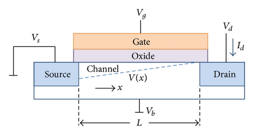
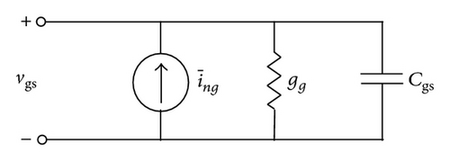
2.2. Modeling Thermal Noise in Short-Channel Devices
2.3. Results and Comparisons of Modeling Noise in Short-Channel Devices
While the expressions for the power spectral density in (11) and (13) include short-channel effects, they are not compatible with the form required by geometric programming. A simpler noise formula which captures the essence of the noise issues at the deep submicron technology nodes is required. As previously noted, the channel thermal noise can be conveniently expressed using the white noise gamma expression given in (6). Since this expression is a simple closed-form equation, it has been widely used for noise analysis by circuit designers. For long-channel MOSFETs, the theoretical values of γ are well known. It is equal to unity at zero drain bias and 2/3 in the saturation region.
The analysis and experimental measurements by Scholten et al. [30] have shown that the channel thermal noise constant γ and the gate current noise parameter β are independent of the operating frequencies up to moderately high frequencies (around 10 GHz), and they are not very sensitive to bias conditions for high bias voltages. However, both parameters are expected to increase as channel lengths scale down in the submicron range. The values of γ are expected to be larger than their theoretical long-channel values due to excess channel thermal noise discussed previously for short-channel MOSFETs. Due to induced gate noise related to channel noise and the increased significance of the resistivity of the gate material at short-channel lengths, the parameter β will experience a similar increase in value.
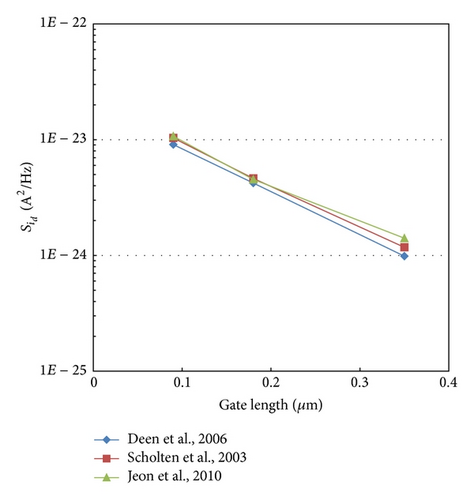
For nanoscale devices with feature sizes below 100 nm, it is still debated whether short-channel effects, as discussed above, are adequate for describing the effects of short-channel noise [44]. Some researchers have suggested that shot noise is better able to describe the noisy behavior for FETs below 40 nm [34, 45, 46]. As this study focuses on LNA design optimization down to the 90 nm node, it will be assumed that excess thermal noise can be adequately handled through modification of the white noise gamma parameter γ. Experimental results from a number of researchers appear to support this approach [31, 34, 43]. A comparison between the expression for the channel thermal noise in (16) [31] with the thermal noise calculation using the two γ models from [30, 43] have been made. As shown in Figure 5 with the numerical data in Table 1, their results are comparable with a similar trend regarding different channel lengths. Since Scholten et al. [30] and Jeon et al. [43] have completed a relatively in-depth study of the noise parameters and there is relatively good agreement of their work with the analytical model of Deen et al. [31], the noise calculations in this work are carried out based upon the results of [30, 43].
3. Optimization Methods
The optimization of the CMOS LNA design in terms of minimizing its noise figure as the main cost function is considered in this section. The maximum allowed power dissipation is used as the main design constraint as this is a chief concern for modern systems, especially those intended for mobile electronic systems. The influence of other design constraints, such as the quality factor of the input circuit and the input impedance matching requirement, is taken into account during the optimization process. The noise analysis of the LNA and the parameters used to model the noise characteristics of submicron MOSFETs are considered first. Then the device equations needed to model the drain current Ids as well as the transconductance gm and the output conductance gd0 are described. Finally, the overall method used to optimize the LNA design within a geometric programming framework is detailed.
3.1. Noise Analysis of the LNA
This subsection describes how the noise figure of the LNA given in Figure 2 can be calculated by small signal analysis. Also, the design parameters used to describe the noise characteristics of short-channel MOSFETs are given. The thermal noise is the major concern at RF intermediate frequencies for MOSFETs. Four noise sources have been considered in this study: the thermal noise of the source resistance (), the channel thermal noise (), the gate noise (), and the thermal noise of the output resistance (). These are depicted in Figure 6. The noise contributions due to the gate resistance are factored into the elevated value for the parameter β as discussed below [30]. Neglecting the effect of the gate-to-drain capacitance Cgd on the noise calculations introduces a small error but allows closed-form equations to be derived. This error is minimized through the use of a cascode topology, where M2 mitigates the Miller effect of Cgd [12]. The noise contributions of the cascode device M2 in Figure 2 are considered to be negligible compared to the contributions of the main FET M1. Following the observations by [30], the noise contributions of the MOSFET source and bulk resistance are taken to be minimal and are neglected in this analysis.
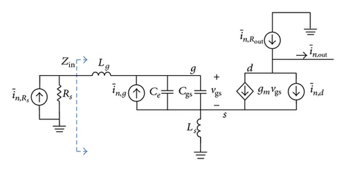
The contributions of these four noise sources referred to the output are denoted by , , , and , respectively. Table 2 summarizes the expressions for these noise sources [9, 47].
| Noise source | Expression | Output-referred expression |
|---|---|---|
| Rs |
|
|
|
|
|
|
|
|
|
|
| Rout |
|
|
Based on the studies by [30, 31, 43], the white noise factor γ is assumed to be independent of the operating frequencies up to 10 GHz and to be independent of bias conditions. A comparison of the values γ versus FET channel length is given in Figure 7.
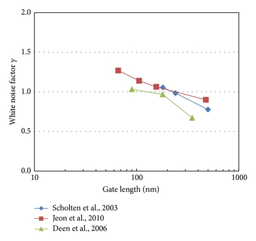
The measured and analytical γ compare favorably when observed at various gate lengths (e.g., 90 nm, 180 nm, and 350 nm), as shown in Figure 7. As expected, the white noise factor γ increases when the channel length decreases. For long-channel devices (channel lengths greater than 1 μm), the traditional value for γ is 2/3.
Numerical values for the gate noise parameter β and correlation coefficient c are estimated from [30, 43] and are summarized, along with the parameter γ, in Table 3. There is a significant increase in the value of the parameter β as the channel length decreases due to the contribution from the gate resistance, which consists of the resistance of the vias, the effective resistance of the silicide, and the contact resistance between the silicide and polysilicon layers [30, 33]. The value of β is close to 4/3 for long-channel devices, but more than doubles in value for 180 nm devices. Therefore, a significant increase is predicted for devices at the 90 nm node. The magnitude of the correlation coefficient is 0.395 for long-channel devices [8], and it decreases due to larger γ and β when channel length reduces in size as can be inferred from (C.3) in Appendix C. A reasonable approximation is that the values for the parameters β and c are relatively independent of frequency and variations with bias conditions for strong inversion. Scholten et al. [30, 48] have shown that modeling the gate noise power spectral density with a constant value for β using (7) gives a good fit to experimentally measured results for short-channel devices over a range of applied voltages up to 10 GHz. They also show that the correlation coefficient c is relatively independent of frequency and bias voltage.
| Parameters | 90 nm design | 180 nm design |
|---|---|---|
| White noise factor (γ) | 1.2 | 1.05 |
| Gate noise parameter (β) | 7.5 | 3.8 |
| Correlation coefficient (c) | 0.2 | 0.2 |
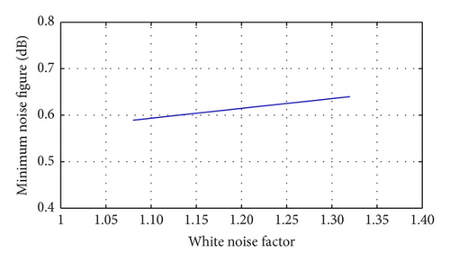
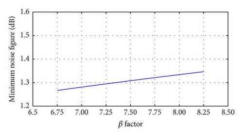
In order to determine the sensitivity to γ and β in the calculation of the minimum noise figure, the effect of varying these parameters was analyzed (see Appendix D for further details). When a ±10% variation is applied to γ, a small percentage of variation (around 4%) occurs to the minimum noise figure. Similarly, less than 4% variation occurs on the minimum noise figure when a ±10% change is applied to β. This gives confidence to the assumption that the parameters γ and β can be modeled as constants for a given technology node without adversely affecting the optimization results.
3.2. Device Equations for Submicron FETs
3.3. Geometric Programming Optimization of the LNA
-
Minimize an objective function: f0(x)
-
subject to constraints:
()
Process-dependent parameters for 90 nm and 180 nm technology nodes were derived from the SPICE model files provided by a predictive technology model (PTM) [49, 50]. Furthermore, the vertical field mobility degradation factor θ, the channel-length modulation parameter λ, and the body effect coefficient m were extracted from the device characterizations provided by running SPICE simulations using the PTM models. The relevant parameters are summarized in Table 4.
| Parameters | 90 nm | 180 nm |
|---|---|---|
| Electron mobility µ0 | 0.0179 m2/V | 0.0288 m2/V |
| Electron velocity saturation vsat | 1.10 × 10⁵ m/s | 9.18 × 10⁵ m/s |
| Oxide capacitance per unit area Cox | 0.014 F/m2 | 0.00857 F/m2 |
| Body effect coefficient m | 1.21 | 1.18 |
| Vertical field mobility degradation factor θ | 0.3 V−1 | 0.2 V−1 |
| Channel-length modulation parameter λ | 0.4 V−1 | 0.3 V−1 |
-
Minimize an objective function: Noise factor F in (20)
-
subject to design constraints:
()
4. Results and Discussion
The optimal design of the CMOS LNA has been computed using CVX, a package for specifying and solving geometric programming problems [51]. The average execution time was about 1.45 seconds on a 3.23 GHz PC with 4 GB memory. The resulting optimal design parameters are shown in Table 5.
| Parameters | 90 nm | 180 nm |
|---|---|---|
| Output conductance (gd0) | 0.0082 S | 0.0063 S |
| Transconductance (gm) | 0.0069 S | 0.0052 S |
| Gate width (W) | 22.172 µm | 27.006 µm |
| Gate length (L) | 90 nm | 180 nm |
| P factor (P = Cgs/Ctot) | 0.1128 | 0.1681 |
| Gate intrinsic capacitance (Cgs) | 18.696 fF | 27.87 fF |
| Additional capacitance (Ce) | 0.147 pF | 0.13792 pF |
| Source inductor (Ls) | 1.2063 nH | 1.5828 nH |
| Gate inductor (Lg) | 25.32 nH | 24.943 nH |
| Drain current (Ids) | 0.5 mA | 0.5 mA |
| Minimum noise figure (Fmin) | 0.6076 dB | 0.8229 dB |
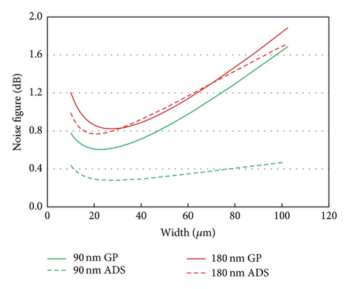
The results from the optimal design using geometric programming have been compared with results from Agilent’s Advanced Design System (ADS) software, a numerical simulation tool used for RF design. The input FET M1 was biased at 0.5 mA and the power supply was set to 2 V with the values of Lg, Ls, and Ce determined by the constraints used in the GP optimization. The output parallel RLC values are calculated by the output circuit quality factor, which is given as 5 in this study. For the 90 nm design, ADS simulations indicate that the minimum noise figure is 0.2799 dB for a gate width of 27 μm, while the optimal width from the optimization of geometric programming is 22.172 μm with a minimum noise figure of 0.6076 dB. For the 180 nm design, a minimum noise figure of 0.7708 dB was obtained for a gate width of 20 μm, while the optimal width from the optimization of geometric programming is 27.006 μm with a minimum noise figure of 0.8229 dB. As shown in Figure 8, the minimum noise figures from the ADS simulations are smaller than the minimum noise figures from the GP results. These discrepancies likely are caused by the lack of implementation of the excess thermal noise in the BSIM3 MOSFET models. The 90 nm design displays relatively larger differences than the 180 nm design, which is not unexpected as excess noise is more significant in shorter channel devices. The optimal widths for minimizing the NF from the GP optimization and ADS simulations are not an exact match, but the overall trends are fairly close. This indicates that geometric programming, which can rapidly find an optimal point, can be used to guide the design of short-channel CMOS LNAs. A good design methodology will then use detailed circuit simulations to fine tune the design and verify its performance. As current simulation models do not adequately account for excess thermal noise, some additional analysis based on experimentally determined FET noise characteristics will be required by the designer to ensure that the optimal design is found.
It should be noted that the inductor value of 25 nH for Lg would not be economical in terms of area when implemented as an on-chip planar spiral inductor. A prudent design choice would be to implement part of the inductance on the chip and the rest through the bond wire; alternatively, one could use the bond wire plus an external inductor on the printed circuit board [1]. Also advances in materials and fabrication technologies have made it possible to embed high quality inductors on the order of 20 nH to 30 nH in a package substrate that are suitable for RF applications [52, 53].
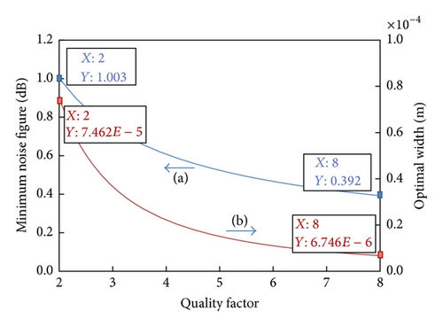
Tradeoff analyses were performed to examine the influence of the quality factor and drain current on the design of short-channel CMOS LNAs. As the optimization results for LNAs designed in 90 nm and 180 nm processes are similar, the trade-off analysis for the 90 nm case is presented in this paper. An inverse relationship is observed between the quality factor and the minimum noise figure, as seen in Figure 9(a). When the input quality factor increases from 2 to 8, the minimum noise figure decreases from 1 dB to 0.39 dB. The quality factor not only affects the minimal noise figure but also influences the optimal width of the LNAs. When the quality factor varies from 2 to 8, the optimal width changes almost 10 times from 75 μm to 6.7 μm, as seen in Figure 9(b). This considerable change in the optimal width indicates the importance of the quality factor in determining the optimal width of M1.
The drain current appears to have great influence on the noise figure when the drain current is at a relatively small scale (i.e., less than 0.5 mA). However, there is not much variation in the noise figure when the drain current increases from 1 mA to 5 mA, as shown in Figure 10. Such an observation is true at different levels of channel width. This suggests that, for this 90 nm process, the best balance between power dissipation, area, and noise figure exists when the LNA is biased with 0.5 to 1.0 mA of current. When the channel width is set to 20 μm, the optimal range for the input circuit quality factor is from 4 to 6. This observation is consistent with the results reported in [9].
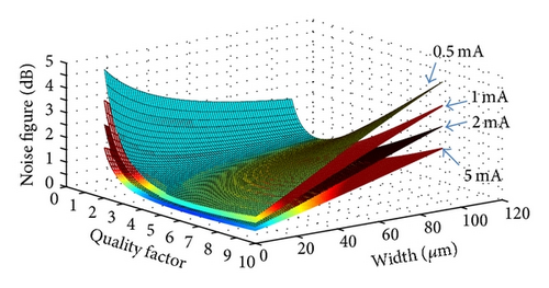
Variations in the frequency of operation also have a significant influence on the noise figure (Figures 11 and 12). In many applications, an RF LNA will be optimized for a particular narrowband of operation, for example, at 2.4 GHz. Therefore, the influence of operational frequency on the noise figure will be limited, and there is a clear choice for the optimum device width for minimizing the noise figure.
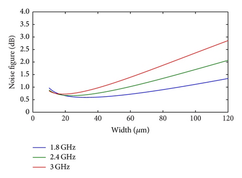
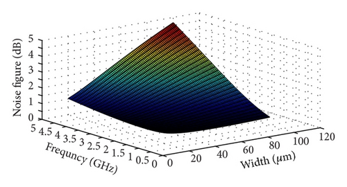
In sum, our results show that the use of geometric programming allows the global optimal design optimization of an LNA to be obtained with great efficiency. This study has focused on the common LNA configuration that uses source inductive degeneration. Short-channel effects have been taken into account when modeling the electronic noise in the MOSFETs as well as in the device characteristics. While some approximations must be made to put the equations in the proper form required by a GP framework, the results are guaranteed to return a globally optimum solution. Various trade-off analyses can be efficiently run as well under given constraints, such as power dissipation and input quality factor. For example, the input circuit quality factor has a great influence on not only the minimum noise figure but also the optimal width. Our results, in general, align well with other results in the literature. In the particular case of the 90 nm technology node used in this study, one can quickly determine the “sweet spot” in the design. The trade-off analyses in this case indicate that the best designs in terms of power and noise figure for the LNA design occur when the drain current is in the range of 0.5 mA to 1 mA with an input circuit quality factor around 5.
5. Summary and Future Directions
This paper has examined the use of geometric programming for obtaining the globally optimum design of RF CMOS LNAs implemented with short-channel devices. The main contribution of this work has been the development of a framework for noise modeling of short-channel devices by including short-channel effects including velocity saturation and channel-length modulation. This noise model forms the basis of the objective function for geometric programming to minimize the noise figure of CMOS LNAs. In addition, the noise figure is minimized subject to the design constraints of input circuit quality factor, power consumption, and input impedance matching. Specific results from the optimization procedure are applied at the 90 nm and 180 nm technology nodes to determine the optimal channel width and noise figure for RF CMOS LNAs. Trade-off analysis indicates some important relationships among the design parameters such as the inverse relationship between noise figure and input circuit quality factor. The relationship between the noise figure and channel width at a given power dissipation and the input circuit quality factor are consistent with simulations from Agilent’s ADS software. The overall design trends are also consistent with other studies reported in the literature. Hence, this study has validated the use of geometric programming as an efficient method to guide the optimal design of CMOS LNAs targeted for implementation at nanoscale technology nodes.
Future work will focus on the enhancement of noise modeling for short-channel CMOS LNAs. For example, the noise contributions from the gate inductor (Lg) and the source inductor (Ls) due to their finite quality factor caused by parasitic effects should be included in the analysis. As devices continue to scale to deep submicron nodes, the doping concentration in the substrate will increase. This affects how the device characteristics are modelled such as the relationship between carrier mobility and diffusivity. In addition, quantum effects should be included when modeling the noise in the channel current [31]. It is expected that more sophisticated equivalent circuit models will be required to model the physical effects of nanoscale devices. The effect of the substrate as a source of noise and the back-gate transconductance in the small signal model should be considered. The thinning of the gate oxide at aggressively scaled technologies may make gate leakage effects an important consideration. Other sources of noise, such as shot noise, should also be taken into consideration below the 40 nm node. The existing noise optimization framework using GP can be modified to include these effects. In addition, the application of GP optimization for other topologies, such as the shunt-series feedback amplifier, will be considered in future work. Finally, with the trend towards biasing analog circuits in the weak to moderate inversion regions to reduce power dissipation, it would be interesting to explore GP methods as outlined in this paper to optimize these circuits.
Conflict of Interests
The authors declare that there is no conflict of interests regarding the publication of this paper.
Appendices
A. Expressions for MOSFET Output Conductance and Transconductance
In this appendix, analytical expressions for the output conductance and transconductance are discussed for both long-channel devices and short-channel devices.
A.1. Derivations of gd0 and gm for Long-Channel Devices
A.2. Derivations of gd0 and gm for Short-Channel Devices
B. Monomial Expressions for gm and gd0
| Parameters | 90 nm | 180 nm |
|---|---|---|
| Gate length L | 0.09 µm ≤ L ≤ 0.45 µm | 0.18 µm ≤ L ≤ 0.9 µm |
| Gate width W | 1 µm ≤ W ≤ 100 µm | 1 µm ≤ W ≤ 100 µm |
| Overdrive voltage Vod | 0.1 V ≤ Vod ≤ 0.4 V | 0.1 V ≤ Vod ≤ 0.5 V |
| Drain to source voltage Vds | 0.5 V ≤ Vds ≤ 1.0 V | 0.6 V ≤ Vds ≤ 1.2 V |
| Parameters | 90 nm | 180 nm |
|---|---|---|
| A0 | 0.0423 | 0.0463 |
| A1 | −0.4578 | −0.4489 |
| A2 | 0.5275 | 0.5311 |
| A3 | 0.4725 | 0.4689 |
| B0 | 0.0091 | 0.0096 |
| B1 | −0.5637 | −0.5595 |
| B2 | 0.5305 | 0.5194 |
| B3 | 0.4695 | 0.4806 |
The accuracy of the curve fitting has been examined by comparing the estimated transconductance (gm) and output conductance (gd0) from the monomial expressions with calculated values from the analytical solutions.
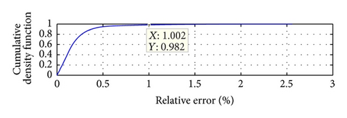
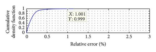
The curve fitting results for the 90 nm process are shown in Figures 13 and 14. The coefficient of determination (R2 value) for the transconductance curve fitting is 0.9999, indicating that the regression fits extremely well with the data compared with the analytical solutions in (23). The maximum relative error from curving fitting is about 2.56% (Figure 13(a)). Furthermore, 98.2% of the curve fitting data has a relative error less than 1.0% (Figure 13(b)).


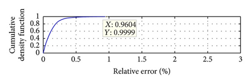
The coefficient of determination for the output conductance is 1.0, suggesting that the curve fitting is close to perfect. The accuracy of curve fitting is shown in Figure 14(a) with a maximum relative error of 0.97%. Moreover, among this curve fitting data, 99.99% of the points have a relative error of less than 0.96% (Figure 14(b)).
The curve fitting results are shown in Figures 15 and 16 for the 180 nm process. The coefficients of determination (R2 value) for these two curve fittings are very close to 1 and more than 97% of curve fitting data have a relative error less than 1.0% for both cases.


C. Expression for the Correlation Coefficient
D. Sensitivity of the γ and β Parameters
This appendix shows the sensitivity of the γ and β parameters on the calculation of the minimum noise figure. The effect of varying the γ parameter is shown in Figure 17. When a ±10% variation is applied to γ, a small percentage of variation (around 4%) occurs to the minimum noise figure. Similarly, less than 4% variation occurs on the minimum noise figure when a ±10% change is applied to β, as illustrated in Figure 18. This gives confidence to the assumption that the parameters γ and β can be modeled as constants for the purposes of optimization.
