On-Chip Power Minimization Using Serialization-Widening with Frequent Value Encoding
Abstract
In chip-multiprocessors (CMP) architecture, the L2 cache is shared by the L1 cache of each processor core, resulting in a high volume of diverse data transfer through the L1-L2 cache bus. High-performance CMP and SoC systems have a significant amount of data transfer between the on-chip L2 cache and the L3 cache of off-chip memory through the power expensive off-chip memory bus. This paper addresses the problem of the high-power consumption of the on-chip data buses, exploring a framework for memory data bus power consumption minimization approach. A comprehensive analysis of the existing bus power minimization approaches is provided based on the performance, power, and area overhead consideration. A novel approaches for reducing the power consumption for the on-chip bus is introduced. In particular, a serialization-widening (SW) of data bus with frequent value encoding (FVE), called the SWE approach, is proposed as the best power savings approach for the on-chip cache data bus. The experimental results show that the SWE approach with FVE can achieve approximately 54% power savings over the conventional bus for multicore applications using a 64-bit wide data bus in 45 nm technology.
1. Introduction
There is a need for high-performance, high-end products to reduce their power consumption. The high-performance systems require complex design and a large power budget having considerable temperature impact to integrate several powerful components. Therefore, low energy consumption is a major design criterion in today’s design. Low energy consumption improves battery longevity and reliability, and a reduction in energy consumption lowers both the packaging and overall system costs [1]. As the technology scaling down the power consumption is also decreasing and results in more sensitivity to soft errors so reliability would be affected. There are tradeoffs between power consumption and reliability in different ways. In future work overall reliability will be discussed and it will be evaluated how it can be improved by reducing the power consumption.
The primary goal of this research is for bus power minimization by reducing the switching activity while at the same time improving bus bandwidth for the compression technique and reducing the bus capacitance for the SW approach. The goal is similar to using switching activity and capacitance reduction in bus power savings; the key difference between the prior work and the work presented here is that the primary focus of this work is to explore a framework for bus power minimization approaches from an architectural point of view. As a result, this paper presents a comprehensive analysis of most of the possible bus power minimization approaches for the on-chip. This research explores a framework for power minimization approaches for an on-chip memory bus from an architectural point of view. It also considers the impact of coupling capacitance for estimating the on-chip bus power consumption. Finally this paper proposes a serialized-widened bus with frequent value encoding (FVE) as the best power savings approach for the on-chip (L1-L2 cache) data bus.
The organization of the rest of the paper is as follows. Section 2 presents background. Section 3 presents framework and proposed on-chip bus power model, a framework for bus power minimization approaches and their efficacy. Section 4 present experiment setup followed by Section 5 which presents the experiment results, a thorough comparison of the proposed technique with the other approaches.
2. Background
Memory bus power minimization techniques can be categorized as bus serialization [2–4], encoding [5–8], and compression techniques [9–14]. Non-cache-based encoding techniques reduce power by reordering the bus signals. Bus serialization reduces the number of wire lines, eventually reducing the area overhead. A serialized-widened bus reduces the capacitance of on-chip interconnections. Cache-based encoding techniques reduce the number of switching transitions using encoded hot-code. These techniques keep track of some of the previous transmitted data using a small cache on both sides of the data bus. Compression techniques reduce the number of wire lines contributing a reduction on in area overhead and an increase in the bus bandwidth. These compression techniques also reduce the switching activity. Serialization changes the data ordering transmitted through the data bus. This method contributes to reducing the switching activity as well. It may also improve the chance of data matching by incorporating it with cache-based encoding techniques because partial data matching is three times more frequent than full-length data matching [7].
Jacob and Cuppu [3] explored the dynamic random access memory (DRAM) system and memory bus organization in terms of performance, presenting design tradeoffs for the bank, channel, bandwidth, and burst size. They also measured the performance in relation to optimize the memory bandwidth and bus width. Suresh et al. [7] presented a data bus transmit protocol called the power protocol to reduce the dynamic power dissipation of off-chip data buses. Hatta et al. [2] proposed the concept of bus serialization-widening (SW) to reduce wire capacitance; their work focused on the power minimization of the on-chip cache address and data bus. Li et al. [15] proposed reordering the bus transactions to reduce the off-chip bus power.
In this chapter we present on-chip bus power model, a framework for bus power minimization approaches and their efficacy. We also discuss in detail the proposed technique and present a thorough comparison of our proposed technique to the possible approaches from power savings stand point.
2.1. Bus Serialization and Widening
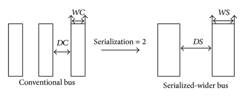
Bus serialization involves reducing the number of wires on the bus. If the number of transmission lines in a conventional bus is NC and the serialization factor is S, then the number of transmission of lines in the serialized version of the bus is given by NS = NC/S. The serialization factor can be any integer multiple of 2. The throughput of a bus serialized by a factor of two is halved. To prevent a reduction in the throughput, the bus frequency can be doubled. This requires the increasing of the wire widths to support higher switching speeds. The advantage of serialization is that the bus occupies less area than a conventional bus. Serialization on its own may not necessarily reduce the switching activity and thus the energy consumption of a bus (see Table 1). Loghi et al. [5] examined the use of bus serialization combined with data encoding for power minimization. In this case, the bus area was smaller, but the throughput of the bus was halved (since the frequency remained the same).
| Passing through 8-bit bus → | Data sequence | Signal | Coupling |
|---|---|---|---|
| 0000 0000 | — | — | |
| 0011 0011 | 4 | 3 | |
| 0011 0011 | 0 | 0 | |
| Total number of transitions | 4 | 3 | |
| Passing through 4-bit bus → | Data sequence | Signal | Coupling |
| 0000 | — | — | |
| 0011 | 2 | 1 | |
| 0011 | 0 | 0 | |
| 0011 | 0 | 0 | |
| 0011 | 0 | 0 | |
| Total number of transitions | 2 | 1 | |
| Passing through - bit bus → | Data sequence | Signal | Coupling |
|---|---|---|---|
| 0000 0000 | — | — | |
| 0011 1100 | 4 | 2 | |
| 0011 1100 | 0 | 0 | |
| Total number of transitions | 4 | 2 | |
| Passing through 4 bit-bus → | Data sequence | Signal | Coupling |
| 0000 | — | — | |
| 0011 | 2 | 1 | |
| 1100 | 2 | 2 | |
| 0011 | 2 | 2 | |
| 1100 | 2 | 2 | |
| Total number of transitions | 8 | 7 | |
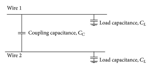
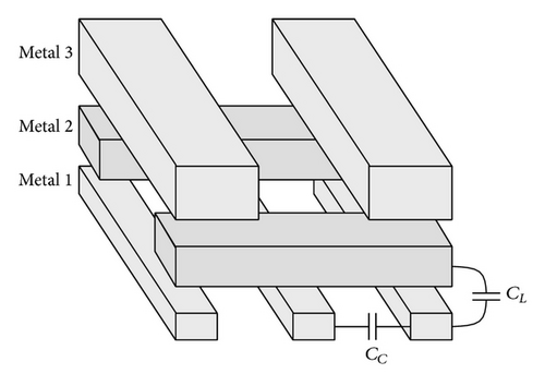
In a deep submicron technology, the switching energy consumed due to coupling capacitance is dominant [16, 17, 24–26]. The disadvantage of bus widening is that the bus occupies more area than a conventional bus. Hatta et al. [2] looked at combining bus serialization with bus widening in order to reduce bus power without increasing the bus area. In that study, the bus frequency was increased to keep the throughput constant. Although this required increasing the width of the wires, the extra spacing between the wires allowed this to be accommodated without a bus area overhead. Hatta et al. [2] also looked at combining a serialized-widened bus with differential data encoding and found that it helped on the address bus but not on the data bus.
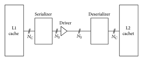
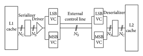
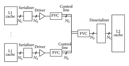
In a serialized-widened bus, the operating frequency can be increased to keep the throughput the same as in a conventional bus. In this case, the serialized frequency is given by fS = S · fC, where S is the serialization factor and fC is the frequency of the conventional bus. In order to implement bus serialization at a higher frequency, a serializer and deserializer are required at the sending and receiving ends of the bus, respectively (as shown in Figure 2).
3. Framework and Proposed Technique
The three fundamental approaches discussed earlier in this section to reduce bus power are serialization (S), encoding (E), and widening (W) of the bus. Combinations of these approaches are also possible, and in fact yield better results. Table 2 lists the possible types of buses based on these three approaches and their combinations (the first of which is a conventional bus (C) not employing any of the approaches). These approaches reduce the power through changes in the switching activity and the line capacitance of the bus.
| Approach | Bus freq. | Switching activity | Line cap. | Bus area | |
|---|---|---|---|---|---|
| 1 | C (conventional) | f | αC | CC | Original bus area |
| 2 | S (serial) | 2f | αS | CS | Reduced |
| 3 | W (widened) | f | αC | CW | At least double |
| 4 | E (encoded) | f | αE | CC | Unchanged |
| 5 | SW | 2f | αS | CSW | Unchanged |
| 6 | SE | 2f | αSE | CS | Reduced |
| 7 | WE | f | αE | CW | At least double |
| 8 | SWE | 2f | αSE | CSW | Unchanged |
Table 2 lists the relation between the switching activity and the line capacitance of the different approaches. It also lists the change in bus area and frequency due to the approaches. Two other important methods to reduce bus power are variations in the swing voltage and operating frequency. These two techniques can be applied in conjunction with all of the methods listed in Table 2. The framework shown in Table 2 can be used to categorize many of the approaches used to minimize the bus switching activity and wire capacitance. The encoding techniques proposed in [12–23, 27–47] fall under the category E listed in the table. The narrow bus encoding technique presented by Loghi et al. [5] falls under the category SE, while Hatta’s serialized-widened bus [2] falls under the category SW.
There are four unique capacitance values and switching activities listed in Table 2. The relation between these capacitance values can generally be described as CW < CSW < CS < CC. If the serialized bus is running at a higher frequency to preserve the bus throughput, the wires and their spacing may have to be widened, thus possibly reducing their capacitance CS from the original bus value, CC. In the widened bus, the wires spacing is increased, making this type of bus having the lowest wire capacitance. However, there is a significant bus area overhead in this approach. The serialized-widened bus running at a higher frequency to preserve the throughput will have slightly less wire spacing than the widened bus since the wires will have to be made wider for the higher frequency. Thus the capacitance of this bus, CSW, will be more than that of the widened bus, CW, but still less than the serialized bus, CS (since the wires are more spaced out than a serialized bus).
The relation between the switching activities is highly dependent on the data values passed on the bus. Therefore a strict relation between the switching activities cannot be shown. However, in general it can be expected that an encoded bus will have less switching than a conventional bus (hence αE < αC). In addition the serialized-encoded bus (SE) will also likely have a lower switching activity than a conventional bus (hence αSE < αC). The relation between the switching activity of a serialized bus (αS) and a conventional bus (αC) is hard to predict.
This paper proposes data bus power reduction techniques for the SWE approach. This work compares these approaches with existing power reduction methods that fall under the different categories in Table 2. This work finds that the SWE approach works best since this method reduces both the wire capacitance and the switching activity significantly.
4. Experimental Setup
This section discusses the target system of the experiment and the memory structure used to collect the memory traces. The first subsection describes the architecture of sim-outorder, the superscalar simulator from the Simplescalar tool suite [48]. In the subsection followed we discusses the benchmarks suite and the input sets that are used in this paper. In the last part of this section we present the switching activity computation methodology.
4.1. Simulator
This experiment uses a modified version of Simplescalar 3.0d’s sim-outorder simulator [48] to collect our cache request traces. The model architecture has mid-range configuration. Table 3 summarizes the architectural configuration of our simulator. The baseline configuration parameters are typical those of a modern chip multiprocessors and out-of-order simulator. This work keeps the L1 cache size smaller to get more memory access which results in more accurate behavior of memory access and memory bus. This work develops another simulator written in program C to calculate the switching activity for the bus power estimation.
| System Parameters | |
|---|---|
| Number of processor cores | 2, 4, 8 |
| Super scalar width | 4, out-of-order |
| L1 instruction cache | 16/32/64 KB, direct-mapped, 1-cycle |
| L1 data cache | 16/32/64 KB, 4-way, 1-cycle |
| L1 block size | 32 B |
| Shared L2 cache | 1 MB, 4-way, unified,, 12-cycle |
| L2 block size | 64 B |
| RUU/LSQ | 16/8 |
| Memory ports | 2 |
| TLB | 128-entries, 4-way, 30-cycle |
| Memory latency | 96-cycle |
| Memory bus width | 1/2/4/8 B |
4.2. Benchmark Suites
This experiment uses 6 integers and 3 floating point benchmarks from SPEC2000 suite [49] and 3 benchmarks from MediaBench suite [47]. This selection is motivated by finding some memory intensive programs (mcf, art, gcc, gzip, and twolf) [3] and some memory nonintensive programs. The simulation wants to use reference inputs of the SPEC2000 suite because of having smaller data sets of test or training inputs. For each of the benchmark of SPEC2000 suite, this work divides the total run length by 5 and warm up for the first 3 portions with a maximum of 2 billion instructions using fast-forward mode cycle-level simulation. A 200 million instruction window is simulated using the detailed simulator. For MediaBench suite, this work simulates the whole program to generate the required traces without any fast forwarding. Table 3 lists the reference inputs that are chosen from the SPEC2000 benchmark and MediaBench suite and the number of instructions for which the simulator is warmed up. Among these benchmarks, a group of benchmarks are selected to run in multicore processor units qs in Table 4. This selection gives importance to group the memory intensive programs to get more accurate behavior of memory access than to group memory nonintensive programs. Table 5 summarizes the list of benchmarks used for 8, 4, and 2 cores processing units.
| Benchmarks | Type | Warm up instructions |
|---|---|---|
| gzip (pro) | Int | 2000 M |
| gzip (src) | Int | 1400 M |
| Wupwise | FP | 2000 M |
| Gcc | Int | 2000 M |
| Mesa | FP | 700 M |
| Art | FP | 2000 M |
| Mcf | Int | 1000 M |
| bzip2 (pro) | Int | 2000 M |
| bzip2 (src) | Int | 2000 M |
| Twolf | Int | 900 M |
| mpeg2d | MB | 0 M |
| Gsm | MB | 0 M |
| mpeg2e | MB | 0 M |
| Number of cores | Set | Name of benchmarks |
|---|---|---|
| 8 | 1 | mcf, art, gcc, twolf, mpeg2d, gzip (pro), mesa, bzip2 (pro) |
| 2 | gzip (src), mcf, gcc, gsm, wupwise, mpeg2e, art, bzip2 (src) | |
| 4 | 1 | mcf, art, mpeg2e, gzip (pro) |
| 2 | twolf, bzip2 (pro), mesa, art | |
| 3 | gcc, gzip (src), bzip2 (src), gsm | |
| 2 | 1 | mcf, art |
| 2 | gcc, twolf | |
4.3. Switching Activity Computation
A power simulator written in C is integrated with the modified Simplescalar sim-outorder simulator [48] to calculate the switching activity of the data transitions between L1 and L2 cache through L1-L2 cache bus. The simulator has several functionalities for calculating the switching activity for all six different kinds of encoding techniques listed in Table 6.
| Name | Abbreviation |
|---|---|
| Bus-invert coding | bi |
| Transition signaling | xor |
| Frequent value encoding with one hot-code | Fv |
| Frequent value encoding with two hot-code | fv2 |
| TUBE with one hot-code | Tube |
| TUBE with two hot-code | tube2 |
During serialization-widening, the simulator uses two sets of value cache (VC) for LSB and MSB data matching instead of using one unified VC. Figure 5 shows the different structures of two sets of VC with serialization. The data bus size is varied frequently to compare the effectiveness of different possible approaches and encoding techniques keeping the total amount of data the same. For example, if a data stream of 64-bit wide requires 1 transition using 64-bit wide data bus, it requires 8 transitions using 8-bit wide data bus.
5. Results and Analysis
This section presents the experimental results. It has a general comparison of the cache bus power minimization using the seven possible approaches listed in Table 2. It further examines in detail three of the approaches that do not change the bus area and finds that the SWE approach performs the best. It also presents an in depth analysis of the SWE approach performance under various architecture and technology configurations. At the end of this section we discuss the performance, power, and area overhead for the proposed technique.
5.1. Power Savings for Different Possible Approaches
The seven possible bus power savings approaches listed in Table 2 earlier are different combinations of serialization (S), bus widening (W), and encoding (E). Figure 6 shows the power savings on the L1-L2 cache data bus for the different architecture-benchmark combinations listed in Table 5 using these approaches. A 64-bit data bus implemented on 45 nm technology is assumed. The techniques reduce bus power by minimizing bus switching activity, bus wire capacitance, or both.
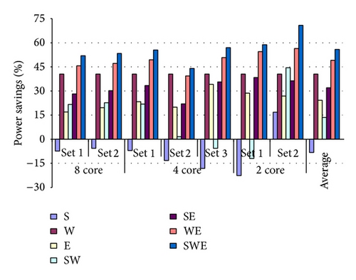
When the three approaches for power reduction are applied on their own, bus widening performs the best. The serialization (S) approach performs poorly for most of the architecture configurations listed in Figure 6 (the bus power is generally increased). This is primarily due to the fact that serialization generally increases switching activity. The bus capacitance is actually reduced partially since the wires are spaced out further to allow the frequency to be doubled. However, this reduction in capacitance is not enough to offset the increased switching activity. The widening (W) approach performs very well since it reduces the bus wire capacitance significantly. The disadvantage of the approach is that it almost doubles the bus area. There are six different encoding techniques (E) that are tested (see Table 6). Figure 6 shows the result from the best encoding technique for each architecture configuration. Encoding reduces switching activity without affecting the bus capacitance and so does minimizing the bus power. This approach does not change the bus area or frequency.
When using combinations of the three approaches, the serialized-widened-encoded (SWE) method performs the best. The serialized-widened (SW) approach reduces the bus capacitance by widening the wire spacing, but generally increases the switching activity through serialization. The net result of these two opposing effects is generally a decrease in the power consumption (although there are cases where power is actually increased). This is the approach proposed by Hatta et al. [2] for both the address and data buses. The serialized-encoded (SE) method reduces the bus power mainly through a reduction in switching activity. There is also a slight reduction in capacitance due to the serialization. The widened-encoded (WE) approach reduces the power by minimizing both the switching activity and bus capacitance. It however has the disadvantage in increasing the bus area. Finally the serialized-widened-encoded (SWE) approach produces the best results for the architectures in Figure 6 by minimizing the bus capacitance and switching activity while keeping the bus area constant.
The rest of this chapter considers primarily the SW, E, and SWE approaches as these do not change the bus area. Unless explicitly stated, a 45 nm technology implementation is assumed.
5.2. Serialization-Widening (SW)
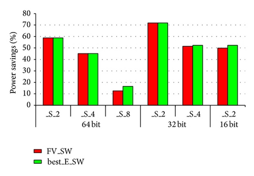
Figure 7(a) shows the power savings of using a serialized-widened bus (as proposed by Hatta et al. [2]) for different bus widths and serialization factors. The results show that the SW approach performs well for narrow buses. Figure 7(b) shows the absolute power consumption of the SW approach with different architectural configurations normalized with a 64-bit wide conventional data bus. The average power consumption of a specific bus width does not vary to each other irrespective of serialization factors.
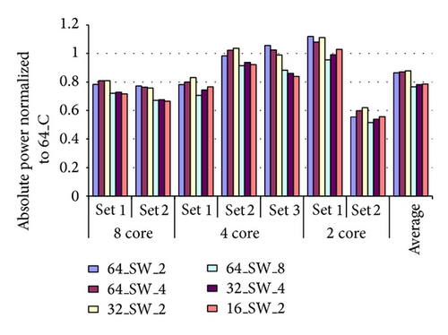
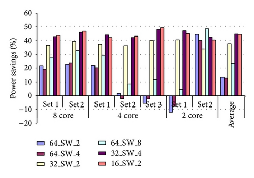
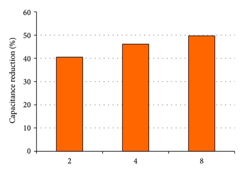
Figure 8 shows the percentage of capacitance reduction using the serialization-widening data bus approach for different serialization factors. The figure shows that a serialization factor of 4 or 8 does not provide a significant reduction of capacitance over a serialization factor of 2.
5.3. Encoding (E)
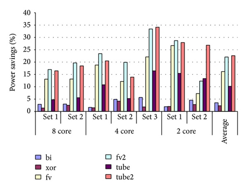
Figure 9 compares the power savings from the different encoding schemes presented in Table 6 for a 64-bit L1-L2 cache data bus. Table 7 shows the power savings of the encoding techniques for various cache bus widths. For the 64-bit and 32-bit wide buses, the frequent value or TUBE approaches with two hot-codes (FV2 and TUBE2) perform the best. This is mainly because the wide bus allows for a large number of entries in these encoding caches. With a 16-bit data bus width, a frequent value cache using one hot-code performs better. This is because the larger cache size of FV2 than FV increases the hit rate, but large number of them hit in the location that requires a switching activity of two instead of one. Table 8 lists the hit rate and the number of one or two transition cache location hit of FV2 and the number of one transition cache location hit of FV for simulating 8-core set 1 application. It is obvious from the data of the table that FV2 performs poorly as large data matching hits in two transition cache locations. An improvement of this situation is to map the most frequent data value in the cache location of smaller number of transitions. This type of encoding technique is proposed by Suresh et al. [7]. It can be easily implemented in advance as their proposed context independent codes works for known dataset of embedded processing systems. But, it requires very complex hardware design to implement for a real-time data arrangement. For the 8-bit cache bus width, none of the cache-based approaches work well as their hit rates are low (since values get replaced too often). In this case bus-invert has the best performance.
| 64-bit | 32-bit | 16-bit | 8-bit | |
|---|---|---|---|---|
| bi | 3.491879 | 13.10983 | 12.55175 | 10.22098 |
| xor | 2.292305 | 7.015497 | 4.343778 | 3.213289 |
| fv | 16.15159 | 38.09723 | 25.42917 | 5.665817 |
| fv2 | 22.04569 | 37.30793 | 17.56435 | 2.736691 |
| tube | 10.20364 | 29.08284 | 9.316818 | 1.79227 |
| tube2 | 22.58817 | 43.95828 | 20.94449 | 2.792153 |
| FV | FV2 | |
|---|---|---|
| Hit rate (%) | 68.08 | 79.87 |
| Number of 1-transition hit | 11586571 | 2047667 |
| Number of 2-transition hit | 0 | 11545453 |
5.4. Serialization-Widening with Encoding (SWE)
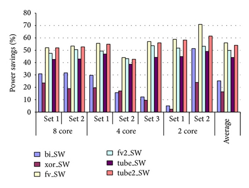
Figure 10 compares the power savings from the different encoding schemes presented in Table 6 using the serialized-widened-encoded (SWE) scheme for a 64-bit L1-L2 cache data bus. Table 9 shows the power savings of the encoding techniques for various cache bus widths and a serialization factor of 2. For the 64-bit and 32-bit wide buses, the frequent value approach (FV) performs the best. This is mainly because the wide bus allows for a large number of entries with a higher number of switching activity (as given example in Table 8) in these encoding caches. With a 16-bit data bus width, a bus invert performs better. This is because we end up with an 8-bit bus after serialization, and the cache hit rates become too low for this configuration.
| 64-bit | 32-bit | 16-bit | |
|---|---|---|---|
| bi | 25.23832 | 35.94936 | 41.25804 |
| xor | 16.42357 | 17.68467 | 22.45874 |
| fv | 55.94778 | 59.1091 | 27.96345 |
| fv2 | 49.89886 | 51.8574 | 10.45392 |
| tube | 44.20373 | 44.15911 | 3.55008 |
| tube2 | 53.97197 | 54.80531 | 10.87319 |
5.5. Power Savings under Different Architecture Options
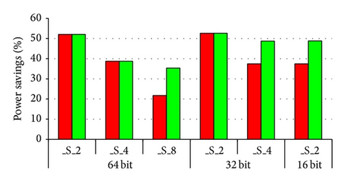
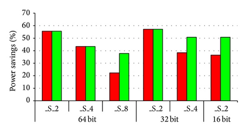
Figure 11 presents the percentage of power savings for the SWE approach using frequent value encoding (FVE) and the best encoding for different bus widths and serialization factors. The amount of power savings achieved by this approach depends on several factors. These factors include cache data bus width, types of applications, number of processing cores, L1 cache size, and type of technology used. For a specified bus width, a serialization factor of 2 with encoding gives more power savings than any other combinations. Although higher serialization factor can contribute in more capacitance reduction, it reduces the number of bus lines. This reduction of the number of bus lines decreases the chance of data matching for cache-based encoding. To choose a cache bus width for L1-L2 cache bus design, Figure 11 gives a comparative view of power savings for different cache bus width using the proposed technique with other best encoding technique. The proposed technique works well for wide data bus, but poorly performs for narrow bus.
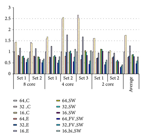
Cache bus power consumption can be varied with bus width, application sets, and different approaches (E, SW or SWE). Figure 12 is a comparative view of cache bus power for a 32 KB L1 cache with 64-/32-/16-bit bus size. The graph shows that a 32-bit wide bus consumes more power than a 64-bit wide bus for most of the application sets used in this experiment. For a 16-bit wide bus, it consumes almost similar or sometimes more power than a 32-bit wide data bus. Encoding (E) approach consumes almost the same amount of power for 64-/32-bit wide data buses. This indicates that the power consumption of the E approach is independent of the bus size. A 16-bit data bus requires a bit higher power than either a 64-bit or 32-bit wide data bus using E approach. SW approach gives us a similar result for the 64-bit and 32-bit data buses. But, a 16-bit data bus requires quite less power than a 64-bit or 32-bit using the SW approach. Using the SWE approach, a 64-bit wide data bus consumes approximately 22% less power than a 32-bit wide data bus for the same application sets. The best encoding that supports the SWE approach is frequent value encoding (FVE). FVE works much better with SWE approach than other cache-based techniques because of the reduced number of bus lines. The value cache size of the cache-based encoding depends on the number of bus lines. The reduced number of bus lines reduces the value cache entry which hurts in a data matching chance for TUBE. For FV2 and TUBE2, it increases the table size to a large number, but the overhead increases yielding a large number of switching activity. Table 10 gives a comparison of value cache size among different cache-based encoding techniques for a 32-bit data bus. The comparison of the same study for the 32-bit and 16-bit data bus gives us a good indication that the SWE approach (FVE as the best encoding) for a 32-bit wide bus consumes approximately 17% less power than that of a 16-bit wide data bus. The results also notice that both SW approach and SWE approach more or less performs the same for a narrow bus (a 16-bit wide data bus).
| Encoding technique | Table size | Max. possible switching activity | |
|---|---|---|---|
| Data size | Number of entry | ||
| FV | 32-bit | 32 | 1 |
| FV2 | 32-bit | 528 | 2 |
| TUBE | 32-bit | 5 | 1 or 2 |
| 24-bit | 5 | ||
| 16-bit | 5 | ||
| 8-bit | 8 | ||
| 16-bit | 16 | ||
| TUBE2 | 32-bit | 30 | 2 or 4 |
| 24-bit | 30 | ||
| 16-bit | 30 | ||
| 8-bit | 68 | ||
| 16-bit | 68 | ||
Reliability is also another concern which points to the need for low-power design. There is a close correlation between the power dissipation of circuits and reliability problems such as electromigration and hot-carrier. Also, the thermal caused by heat dissipation on chip is a major reliability concern. Consequently, the reduction of power consumption is also crucial for reliability enhancement. As a future work, we will be working in another paper to evaluate constraint on reliability and power.
5.6. Different L1 Cache Size
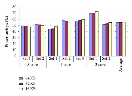
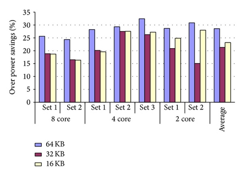
Figure 13 gives a comparison of the absolute power savings of using a 64-bit wide data bus with SWE (FVE) approach having 64 KB, 32 KB, and 16 KB L1 cache size. According to the results, the cache size does not affect in power savings of the proposed technique. Although the cache size can change the order of data transitions through the cache bus, the proposed technique works well irrespective of the changing of data transitions transmitted through the data bus. Thus, this proposed approach keeps consistent result with the variation of L1 data cache size. This figure also compares the percentage of relative power savings of using a 64-bit wide bus compared to a 32-bit bus for the same L1 cache size. Different bus size may change the ordering of the same data set and can significantly affect the number of switching activity. So, changing the cache size alters the data requests from the lower level cache and passing the data requests using different bus width may revise the number of switching activity. This effect can visualize from the Figure 13(b) but still it favors a 64-bit wide data bus from a power saving standpoint compared to a 32-bit wide data bus.
5.7. Different Technologies
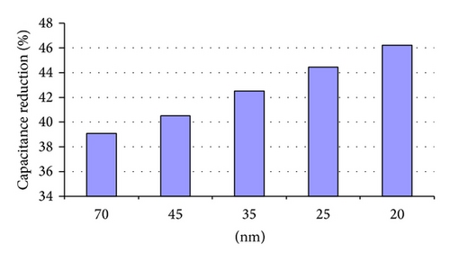
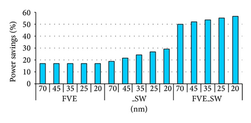
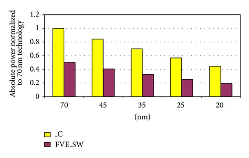
This work extends the experiment for different technologies not keeping limited to different cache bus width and L1 cache size. As industry is already started to manufacture for less than 65 nm process technology, the experiment considers small gate size as 70, 45, 35, 25 and 20 nm technology. The experiment finds the capacitance reduction for different technology as shown in Figure 14. Figure 15(a) presents a comparison of the power savings using encoding, serialization-widening, and serialization-widening with FVE. The results shown in Figure 15 uses a 64-bit wide data bus for application set 1 in 8 processing cores. The amount of power savings is in similar fashion for different technologies, but the absolute power consumption reduces with shrinking the technology as shown in Figure 15(b). This is because the swing voltage reduces with shrinking the technology [27]. Although shrinking the technology increases the capacitance (capacitance, C = ε*A/d), serialization-widening gives us the advantage of using extra space between the wires which reduces the overall capacitance compared to the conventional bus and finally reduces the total power budget. Using this advantage, the proposed approach improves the power savings significantly.
5.8. Split Value Cache versus Unified Value Cache
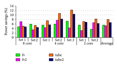
Frequent value encoding (FVE) uses a unified value cache (VC) to implement the VC structure. The size of the VC depends on the type of pattern matching algorithm (full or partial) and type of hot-code (one or two) used in the implementation. In the proposed technique, the simulation uses two sets of VC instead a unified from the VC entry. Figure 16 presents a comparison of the power consumption VC. Two sets of VC hold the least significant bits (LSB) and most significant bits (MSB) part of the data value for implementing serialization-encoding approach as serialization breaks the whole data sequence. Utilization of two sets of VC increases the chance of hits in the VC. This also keeps consistent of the two separate VC as LSB part changes more frequent than MSB part. This removes the necessity of a frequent replacement using these two types of VC implementation. The figure shows that using two separate VC structure gives approximately 5% of more power savings for FVE-based technique and 8% for TUBE than using one unified VC.
5.9. Widened-Encoded Data Bus of 32 Bit Wide
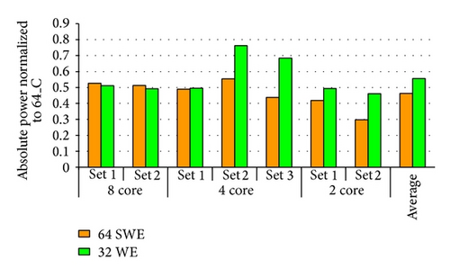
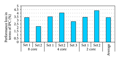
A widened-encoded (WE) 32-bit wide data bus requires the same area as the SWE approach of a 64-bit wide. The results of Figure 6 show that WE approach works very close to SWE approach in power savings. But, the 64-bit wide WE data bus requires double area. This motivates us to compare the power consumption of the WE approach having a 32-bit data bus compared to the SWE approach having a 64-bit wide data bus. Figure 17(a) gives the absolute power consumption normalized with the 64-bit wide conventional data bus. The results show that these two approaches consume almost the same amount of power. The benefit of using WE approach is that it does not require higher operating frequency. But, it has to pay performance loss in terms of IPC for using narrow data bus. The experimental results having the performance loss are shown in Figure 17(b).
5.10. Performance Overhead
Performance overhead is a considerable issue in designing a serializer with frequent value cache (FVC) unit. Figure 18 presents the architectural configuration of a serializer-deserializer with the FVC unit between the L1-L2 cache block.
Hatta et al. [2] presented a novel work about bus serialization-widening and showed that the serialized-widened bus operates in faster frequency than the conventional bus. Liu et al. [32] talked about pipelined bus arbitration with encoding to minimize the performance penalty which might be less than 1 cycle. Although most of the works supports minimized performance penalty using serialization-widening with frequent value technique, it takes 2 cycles penalty in worst case. This work runs the simulation using 2 cycles and 1 cycle performance penalty for L2 data cache access using different application sets. The results present the performance loss in Figure 19. This work further includes a comparative view of absolute power savings using a 64-bit wide bus with serialization-widening and frequent value encoding for 32 KB L1 cache size at 45 nm technology.
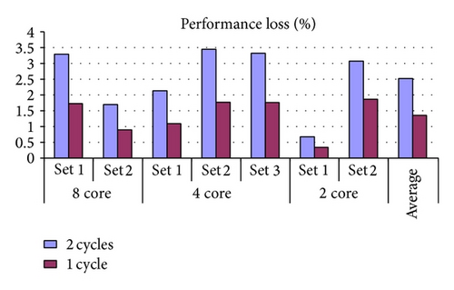
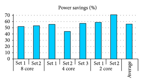
According to the dataset of Figure 19, about 2.5% average performance loss for worst case (2 cycle penalty) if the approach cannot achieve the advantages of faster serialized bus and pipelining in data transmission. This comes down to average 1.35% performance degradation for 1 cycle penalty. Further investigation looks into the area required for additional circuitry. Different citations find that a minimum of approximately 0.05 mm2 area is required to implement the value cache with serializer. The additional peripheral also consumes extra 2% power required by the wire [2, 7, 35].
6. Conclusion
In system power optimization, the on-chip memory buses are good candidates for minimizing the overall power budget. This paper explored a framework for memory data bus power minimization techniques from an architectural standpoint. A thorough comparison of power minimization techniques used for an on-chip memory data bus was presented. For on-chip data bus, a serialization-widening approach with frequent value encoding (SWE) was proposed as the best power savings approach from all the approaches considered.
- (i)
The SWE approach is the best power savings approach with frequent value encoding (FVE) providing the best results among all other cache-based encodings for the same process node.
- (ii)
SWE approach (FVE as encoding) achieves approximately 54% overall power savings and 57% and 77% more power savings than individual serialization or the best encoding technique for the 64-bit wide data bus. This approach also provides approximately 22% more power savings for a 64-bit wide bus than that for a 32-bit wide data bus using 32 KB L1 cache and 45 nm technology.
- (iii)
For a 32-bit wide data bus, the SWE approach (FVE as encoding) gives approximately 59% overall power savings and 17% more power savings than a 16-bit wide bus for the same L1 cache size and technology.
- (iv)
For different cache sizes (64 KB L1 cache size and 45 nm technology), a 64-bit wide data bus gives approximately 59% overall power savings and 29% more power savings than for a 32-bit wide data bus using the SWE approach with FV encoding.
In conclusion, the novel approaches for on-chip memory data bus minimization were presented. The simulation studies for the same process node indicate that the proposed techniques outperform the approaches found in the literature in terms of power savings for the various applications considered. The work in this paper primarily involved the software simulation of the proposed techniques for bus power minimization considering performance overhead. As far as future work, we will continue to evaluate the proposed approach with lower process node (14 and 10 nm) for reliability especially with new process.
Conflict of Interests
The authors declare that there is no conflict of interests regarding the publication of this paper.


