Improvement in Brightness Uniformity by Compensating for the Threshold Voltages of Both the Driving Thin-Film Transistor and the Organic Light-Emitting Diode for Active-Matrix Organic Light-Emitting Diode Displays
Abstract
This paper proposes a novel pixel circuit design and driving method for active-matrix organic light-emitting diode (AM-OLED) displays that use low-temperature polycrystalline-silicon thin-film transistors (LTPS-TFTs) as driving element. The automatic integrated circuit modeling simulation program with integrated circuit emphasis (AIM-SPICE) simulator was used to verify that the proposed pixel circuit, which comprises five transistors and one capacitor, can supply uniform output current. The voltage programming method of the proposed pixel circuit comprises three periods: reset, compensation with data input, and emission periods. The simulated results reflected excellent performance. For instance, when ΔVTH = ±0.33 V, the average error rate of the OLED current variation was low (<0.8%), and when ΔVTH_OLED = +0.33 V, the error rate of the OLED current variation was 4.7%. Moreover, when the I × R (current × resistance) drop voltage of a power line was 0.3 V, the error rate of the OLED current variation was 5.8%. The simulated results indicated that the proposed pixel circuit exhibits high immunity to the threshold voltage deviation of both the driving poly-Si TFTs and OLEDs, and simultaneously compensates for the I × R drop voltage of a power line.
1. Introduction
The most critical advantage of organic light-emitting diode (OLED) displays over conventional liquid crystal displays (LCD) is that OLED displays do not require backlight module systems. OLED displays can exhibit high contrast, wide viewing angle, fast response time, and low power consumption. Moreover, OLED panels can be thinner and lighter than LCD panels [1–3]. OLED displays are currently designed to use passive-matrix (PM) or active-matrix (AM) modes. PM-OLED displays use a grid to supply charges to a pixel, and AM-OLED displays use low-temperature polycrystalline-silicon thin-film transistors (LTPS-TFTs) to provide a driving current. AM-OLED displays are becoming increasingly popular because they provide more favorable high image contrast and performance than PM-OLED displays do [1]. Moreover, AM-OLEDs have the advantage of using less driving current compared with PM-OLEDs, which can increase the lifetime of OLED materials [1].
AM-OLEDs differ from LCDs because the value of the current flowing through the lighting element controls the luminance of each lighting element; that is, AM-OLEDs use current-controlled lighting elements. Thus, the brightness of an OLED is proportional to the amount of current passing through the diode. To obtain a uniform distribution of brightness, AM-OLED displays must uniformly deliver current to the OLED. However, the inevitable variation in the excimer laser annealing (ELA) process, which is used to form the poly-Si channel, causes a wide variety of electrical characteristics in individual LTPS-TFTs, resulting in a nonuniform driving current [4]. Furthermore, electrical performance degradation of AM-OLEDs caused by long-term operation decreases their brightness, which can be the threshold voltage degradation of driving TFTs (DTFTs) and OLEDs in a pixel circuit [5, 6]. The voltage drop across the parasitic resistance of a power line, called I × R (current × resistance) drop voltage, also causes nonuniform brightness in AM-OLED panels [7]. These differences in the threshold voltages of DTFTs and OLEDs and the I × R drop voltage of a power line cause different currents flowing into the OLED among the pixels. Tightening the threshold voltage variation and preventing the luminance degradation of OLEDs are very crucial to AM-OLED technology. It is reported that the two-TFT and one-capacitor (2T1C) pixel circuit suffers from pixel-to-pixel luminance nonuniformity because of the threshold voltage variation of DTFTs (shown in Figure 1). This issue is exacerbated as the size of a display increases. Instead of improving TFT processes, several studies have attempted to reduce the brightness variation across display panels by altering pixel circuit designs, which can use voltage driving, current driving, and digital driving compensation approaches [8–15]. The current driving method can minimize the shift in the DTFT threshold voltage; however, it requires a longer pixel charging time than that of voltage driving method because of the high parasitic capacitance of a data line. The digital compensation has two methods, such as area ratio grayscale method and time ratio grayscale method. These two methods have an advantage that OLED current can be partly uniform against the variation of the DTFT characteristic. However, the grayscale numbers of area ratio grayscale method and time ratio grayscale method are limited by the subarea number and the subframe number, respectively. Nowadays, the grayscale of display has already become a huge amount, so the digital methods were not suitable for application on the high resolution for AMOLED [15]. The voltage driving method can effectively manage the threshold voltage shift and also solve the nonuniform brightness problem. However, most studies have not simultaneously compensated for the threshold voltage variation of DTFTs and OLEDs and the I × R drop voltage [8–15].
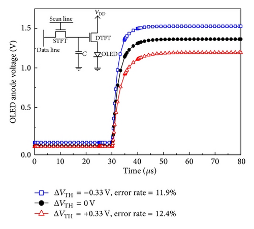
This paper proposes a novel voltage programming AM-OLED pixel circuit to produce displays with uniform brightness. The proposed pixel circuit, which comprises five n-type LTPS-TFTs and one capacitor, can compensate for the nonuniformity of OLED currents caused by the threshold voltage variations of DTFTs and OLEDs. The pixel circuit can also simultaneously compensate for the OLED luminance degradation caused by the I × R drop voltage of a power line. The simulation results indicated that the proposed pixel circuit successfully supplies a highly stable OLED current and is suitable for larger AM-OLED displays.
2. Operation of the New Proposed Voltage Programming Pixel Circuit
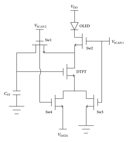
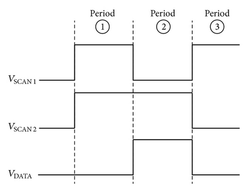
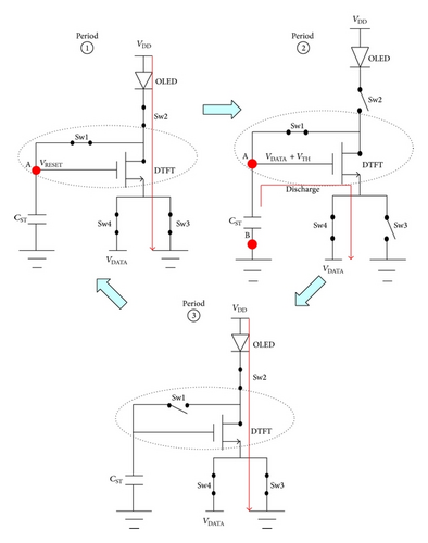
To achieve a stable OLED current even through the DTFTs and OLEDs producing threshold voltage variations, a five-TFT and one-capacitor pixel circuit was designed. Figure 2(a) shows a schematic of the proposed pixel circuit, which includes one DTFT, four switching TFTs (Sw1 to Sw4), one storage capacitor (CST), one OLED, and three signal lines (VSCAN1, VSCAN2, and VDATA). Sw1 is used to turn the DTFT into a diode-connected structure; Sw2 detects the voltage between the gate and the drain (VGD) in the DTFT; Sw3 controls the emission stage of the OLED; Sw4 is used to control data input. VSCAN1 and VSCAN2 are the control signals used to turn the switching TFTs (Sw1 to Sw4) on or off. VDATA represents a data-voltage signal and VDD refers to a constant-voltage source. The control-signal timing diagram for the proposed circuit is divided into three stages, as shown in Figure 2(b). The three circuit operations stages are Periods ①, ②, and ③, which refer to a reset period, a compensation period with data input, and an emission period, respectively. The equivalent circuits at each operation stage are shown in Figure 3. The operational method and compensation principle that apply to the proposed pixel circuit are described as follows.
2.1. Reset Period
The functions in this stage are precharging and resetting the voltage stored in CST. VSCAN1 and VSCAN2 are high and VDATA is low; therefore, Sw1, Sw2, Sw3, and Sw4 are turned on. The voltage located at Node A is charged toVRESET through Sw1 and Sw2. The voltage previously stored in CST is reset; therefore, the gate voltage of the DTFT connected to CST is also reset for initialization. This stage can be used to reset gate voltage of DTFT which is composed of the VDATA and the compensated voltage in the previous emission period. In addition, the charging current will flow through the OLED in the reset period to cause the decreased contrast ratio except that extra scan lines for switch TFTs are added in the circuit [11, 16].
2.2. Compensation Period with Data Input
In this stage, the threshold voltage of the DTFT (VTH) is detected by the compensation operation. When VSCAN1 returns to a low value, Sw2 and Sw3 are turned off. When VSCAN2 remains high, Sw1 and Sw4 stay on. At this moment, when a data voltage (VDATA) is applied, the voltage at the source electrode of DTFT becomes VDATA and the gate electrode of DTFT is charged to a higher potential, which is sufficiently high not to interfere with the compensation operation at this stage. Hence, the gate voltage of DTFT (VA) is discharged through Sw1, DTFT, and Sw4 until the DTFT is turned off. The gate voltage of DTFT that has a diode-connect structure reaches VDATA + VTH, where VTH is the DTFT threshold voltage. Because Node B is set to ground, the voltage across CST can be written as VA − VB = VDATA + VTH.
2.3. Emission Period
3. Simulation Result and Discussion
AIM-SPICE was used to simulate the proposed pixel circuit to investigate the compensation capability of the threshold voltage shifts of DTFTs and OLEDs. The AIM-SPICE poly-Si TFT model, poly-Si TFT model PSIA2 (level 16), was used in the simulation. The OLED was modeled using a diode-connected poly-Si TFT and a capacitor. Table 1 shows the simulation parameters. The simulated I-V curves of the poly-Si TFT (DTFT) and OLED with the parameters of Table 1 are shown in Figures 4(a) and 4(b), respectively.
| Devices | |||
|---|---|---|---|
| W/L (Sw1~Sw4) (μm) | 8/2 | VTH (DTFT) (V) | 1 |
| W/L (DTFT) (μm) | 12/2 | VTH_OLED (OLED) (V) | 1 |
| CST (pF) | 0.35 | COLED (pF) | 1 |
| μ FET (cm2/Vs) | 51.48 | ||
| Signal line | |||
| VSCAN1 (V) | −3 to 15 | V DATA (V) | 1 to 4.5 |
| VSCAN2 (V) | −3 to 15 | V DD (V) | 12 |
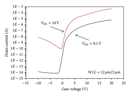
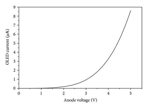
Figure 5 shows the transient waveforms of each DTFT node when the data voltage (VDATA) is 3 V. At the compensation stage with data input (Period ②), the DTFT gate voltage is discharged to VDATA + VTH = 4 V, where VTH is the DTFT threshold voltage. During the emission stage (Period ③), the DTFT gate voltage is maintained at 4 V (VDATA + VTH) as the DTFT VGS. Thus, the proposed circuit successfully compensates for the threshold voltage degradation of DTFTs and OLEDs. Figure 6 shows the simulated transient results obtained by varying the DTFT threshold voltage (ΔVTH = − 0.33, 0, and + 0.33 V). The OLED cathode voltage was insensitive to the DTFT threshold voltage deviation. The error rates of the OLED cathode voltage when ΔVTH = 0 and ±0.33 V were all below 0.03%. Therefore, the current flowing through the OLED was uniform. Thus, the proposed pixel circuit reduced the effect of DTFT and OLED threshold voltage deviations.
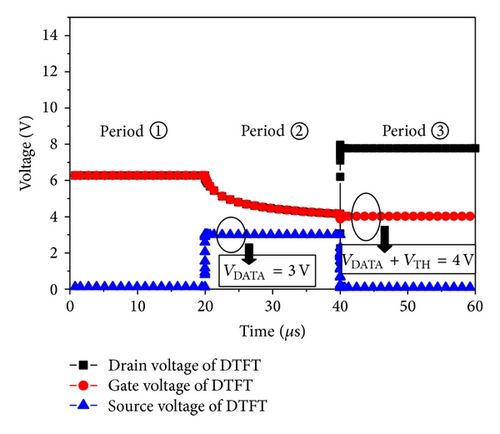
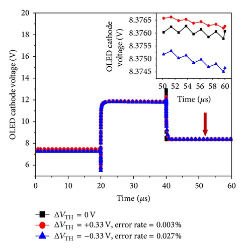
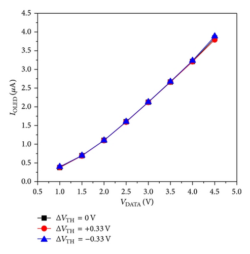
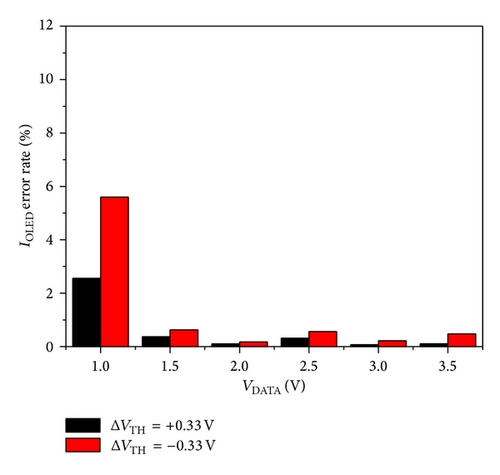
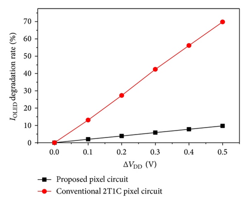
Figure 8 presents the simulation results of the IOLED degradation rates of the proposed circuit and the conventional 2T1C pixel circuit when the range of the I × R drop voltage of a power line (ΔVDD) is 0.5 V. The initial VDD value was set to 12 V and the I × R drop voltage (ΔVDD) was set to 0.5 V; that is, the VDD decayed from 12 V to 11.5 V. In conventional 2T1C pixel circuit, the IOLED degradation rate is approximately 70% to 80%. The proposed pixel circuit can improve the IOLED degradation rate caused by the I × R drop voltage of a power line. In addition, the IOLED degradation rate when ΔVDD was 0.3 V improved to approximately 5.8%. This demonstrates that the proposed pixel circuit can effectively solve the issue of I × R drop voltage.
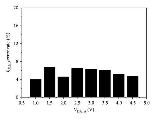
Figures 9(a) and 9(b) present the IOLED value and its error rate when the degradation of the OLED threshold voltage (ΔVTH_OLED ) is +0.33 V at a range of data voltages between 1 V and 4.5 V, respectively. After long-term operation, the OLED threshold voltage (VTH_OLED) increases, causing the brightness and quality of the display to deteriorate. As shown in Figure 9(b), the proposed pixel circuit can compensate for OLED degradation and the average IOLED error rate was 4.7%. Therefore, the display image uniformity improved as a result of the decreased IOLED error rate.

4. Conclusions
This study proposed a voltage programming pixel circuit for AM-OLED displays and verified the circuit using the AIM-SPICE simulator. The proposed circuit was composed of five TFTs and one capacitor and it simultaneously compensated for the threshold voltage variations of DTFTs and OLEDs and the I × R drop voltage of a power line. The simulation results demonstrated that the average error rates of the OLED current when ΔVTH = ± 0.33 V for DTFTs and ΔVTH_OLED = + 0.33 V for the OLEDs were less than 1% and 5%, respectively. The average error rate was also less sensitive to the I × R drop voltage of a power line. Therefore, the proposed circuit exhibited high immunity to the threshold voltage deviation of both DTFTs and OLEDs and improved the brightness uniformity of AM-OLED displays.
Conflict of Interests
The authors declare that there is no conflict of interests regarding the publication of this paper.
Acknowledgments
The authors would like to acknowledge the financial support of the National Science Council of Taiwan under Contract nos. NSC 101–2221-E-011-070 and NSC 102–2221-E-011-112-MY2 and of the Taiwan Building Technology Center (TBTC) of National Taiwan University of Science and Technology (NTUST).


