60Co-Gamma Ray Induced Total Dose Effects on P-Channel MOSFETs
Abstract
Total Dose Effect (TDE) on solid state devices is of serious concern as it changes the electrical properties leading to degradation of the devices and failure of the systems associated with them. Ionization caused due to TDE in commercial P-channel Metal Oxide Semiconductor Field Effect Transistors (MOSFETs) has been studied, where the failure mechanism is found to be mainly a result of the changes in the oxide properties and the surface effects at the channel beneath the gate oxide. The threshold voltage of the MOSFETs was found to shift from −0.69 V to −2.41 V for a total gamma dose of 1 Mrad. The net negative threshold shifts in the irradiated devices reveal the major contribution of oxide trapped charges to device degradation. The radiation induced oxide and interface charge densities were estimated through subthreshold measurements, and the trap densities were found to increase by one order in magnitude after a total gamma dose of 1 Mrad. Other parameters like transconductance, subthreshold swing, and drain saturation current are also investigated as a function of gamma dose.
1. Introduction
In recent years, one can observe a tremendous increase in the usage of electronic instrumentation for nuclear and space research, and it is often susceptible to high ionizing radiations in space. Considerable attention must therefore be given to possible effects of such an environment on electronic devices. Gamma rays are one of the basic radiation sources used to test the device for space applications. Gamma rays interact with matter in three different ways: photoelectric effect, compton scattering, and pair production. In silicon, the photoelectric effect dominates at photon energies less than 50 keV, and pair production dominates at energies greater than 20 MeV with Compton scattering dominating in the intervening energy range [1]. MOSFETs being widely used in space systems because of their faster switching speeds and simple drive requirements are very sensitive to ionizing gamma radiations. The high threshold voltage shifts caused due to trapped charges reduce the switching speed and also modify the other charge dependent properties like transconductance and mobility [2, 3]. The ionization effects in these devices can be related to either the total amount of radiation that is absorbed (total dose) or the rate at which radiation is absorbed (dose rate) [4]. In the present experiment, the devices are evaluated for total dose effects.
Of most concern in the total dose effects is the creation of hole electron pairs in silicon dioxide. In any silicon technology in which silicon dioxide is in contact with low acceptor doped (p-type) silicon, concern for total dose effects is warranted. The dominant effects are due to holes being trapped at the oxide causing free electrons to be attracted to the Si–SiO2 interface and effectively resulting in an inversion of the doping near the interface [5]. Thus, the electrons in the region between the two p-regions of a p-channel MOSFET cause leakage currents and change the electrical parameters of the MOSFETs. In addition to hole trapping, interface states are also generated at Si–SiO2 interface. When a negative bias is applied to the gate of a p-channel MOSFET, positive interface charges cause the threshold voltage to shift towards less negative side, while negative interface charges cause threshold voltage to shift towards the more negative side. Holes transporting through p-channels undergo Coulomb scattering from the charged interface states resulting in reduction in carrier channel mobility and increase in channel ON resistance.
2. Devices and Methods
The 60Co-gamma irradiation was performed on ALD1102 P-channel MOSFETs using the Blood Irradiator-2000 at ISRO Satellite Centre, Bangalore. The Gamma irradiator (Blood Irradiator-2000) has a Cobalt-60 source capacity of 675 Ci with photon energies 1.17 MeV and 1.33 MeV. The devices were irradiated for different doses varying from 1 krad to 1 Mrad. All the leads of the devices were shorted and grounded during irradiation as P-channel MOSFETs are very sensitive to even the smallest parasitic currents. The effects of 60Co-gamma rays on P-channel MOSFETs were studied for changes in the threshold voltage (VT), transconductance (gm), drain current (ID), subthreshold swing (S), oxide charge density (Not), and interface charge density (Nit).
2.1. Charge Separation Method
3. Results and Discussion
Current-voltage (I-V) characteristics at room temperature were carried out on ALD1102 MOSFETs using Keithley I-V Source Measure Units. The devices were characterized for ID-VDS and ID-VGS characteristics before and after irradiation with various doses of gamma rays. The changes in the threshold, subthreshold, and transfer characteristics are analyzed and reported.
3.1. ID-VGS Characteristics
Threshold voltage is extracted from ID-VGS characteristics by keeping the drain-source voltage (VDS) constant at −8 V. Figure 1 shows the ID-VGS curves of virgin and gamma irradiated devices. It can be noticed that the curve shifts towards more negative voltage with increase in gamma dose.
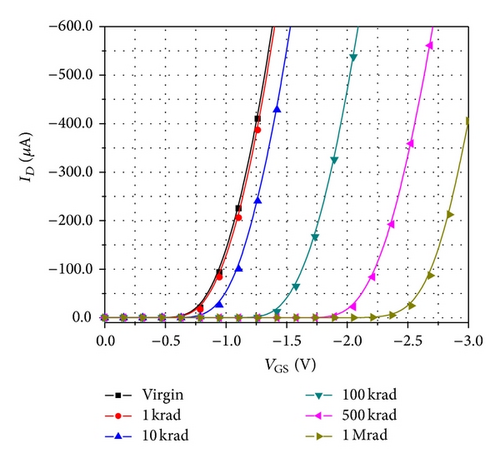
The threshold voltage of the devices was found to be −0.69 V for unirradiated (virgin) device and shifted to −2.41 V for device irradiated to a total gamma dose of 1 Mrad. The negative shift in the threshold voltage can be attributed to the buildup of positive oxide charges. Even though the interface charges contribute to the shift in the threshold voltage, the effect of oxide charges dominates. The individual contributions of oxide and interface charges for the threshold voltage shift are reported in Table 2. The gm is directly related to the drain current and is one of the important parameters of a MOSFET. A high gm is always preferred when it comes to transistor performance. The transconductance of P-channel MOSFETs was found to decrease from 30.90 × 10⁻⁴ mho (virgin) to 4.04 × 10⁻⁴ mho for a total gamma dose of 1 Mrad. The decrease in transconductance is the result of decreasing slope in the saturation region of ID-VGS curves [13].
3.2. ID-VDS Characteristics
The drain saturation current (IDsat ) is extracted from ID-VDS characteristics by keeping the gate-VGS constant at −6 V. Figure 2 shows the ID-VDS curves of virgin and gamma irradiated devices. It can be noticed that the drain current saturates early with the increase in gamma dose. The drain saturation current is measured at a particular point on the ID-VDS curve in the saturation region.
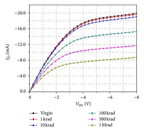
The IDsat was found to be −19.06 mA for virgin device and reduced to −8.13 mA for device irradiated to a total gamma dose of 1 Mrad. The reduction of drain current due to gamma exposure can, in principle, be explained by a shift of threshold voltage (VT) and/or a decrease of mobility (μ) [14]. The reduction in the drain current can also be attributed to the increased channel resistance caused due to carrier removal effect in irradiated devices. The pronounced Coulomb scattering in the channel due to radiation induced interface traps also causes the drain current to reduce.
3.3. Subthreshold I-V Characteristics
Figure 3 shows the subthreshold characteristics of virgin and gamma irradiated P-channel MOSFETs.
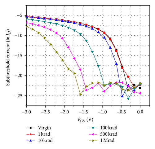
The decrease in slope of ln ID versus VGS curves with increase in total dose can be clearly observed. The slope of the preirradiated curve was measured to be 26.66, while the one irradiated to a total gamma dose of 1 Mrad was found to be 11.04. The decreasing slope was analogous to the distortion of the C-V characteristics and is due to an increase in the density of interface traps [13]. A decreased slope means that a larger swing in gate voltage is required to bring the transistor into strong inversion. Therefore, interface traps reduce the switching speed of MOSFETs. The subthreshold swing is found to increase from 9.0 mV/decade (virgin) to 16.10 mV/decade for a total gamma dose of 1 Mrad.
The experimentally obtained values of threshold voltage (VT), transconductance (gm), subthreshold swing (S), and drain current (ID) for virgin and gamma irradiated devices are summarized in Table 1.
| γ-Dose | VT (V) | gm (×10−4 mho) | S (mV/decade) | ID (mA) |
|---|---|---|---|---|
| Virgin | −0.69 | 30.90 | 9.0 | 19.06 |
| 1 Krad | −0.72 | 30.60 | 9.62 | 18.81 |
| 10 Krad | −0.84 | 29.30 | 10.12 | 18.17 |
| 100 Krad | −1.39 | 21.32 | 10.58 | 14.63 |
| 500 Krad | −1.95 | 11.07 | 13.34 | 11.12 |
| 1 Mrad | −2.41 | 4.04 | 16.10 | 8.13 |
| γ-Dose | ΔVT (V) | ΔVot (V) | ΔVit (V) | ΔNOT (cm−2) | ΔNIT (cm−2) |
|---|---|---|---|---|---|
| 1 Krad | −0.03 | −0.041 | 0.011 | 3.00 × 10¹⁰ | 8.33 × 10⁹ |
| 10 Krad | −0.15 | −0.169 | 0.019 | 1.23 × 10¹¹ | 1.44 × 10¹⁰ |
| 100 Krad | −0.7 | −0.727 | 0.027 | 5.27 × 10¹¹ | 2.00 × 10¹⁰ |
| 500 Krad | −1.26 | −1.333 | 0.073 | 9.67 × 10¹¹ | 5.36 × 10¹⁰ |
| 1 Mrad | −1.72 | −1.840 | 0.120 | 1.33 × 10¹² | 8.72 × 10¹⁰ |
3.4. Oxide and Interface Trapped Charges Density
The effect of oxide and interface charges on the threshold and subthreshold characteristics of a MOSFET has been briefed in the earlier sections. As discussed before, both the charges (oxide and interface) contribute to the total threshold voltage shift (ΔVT), and the individual contribution to the ΔVT can be identified by using the charge separation technique. Figure 4 shows the total voltage shift and the voltage shifts due to oxide (ΔVot) and interface trapped charges (ΔVit) for various doses of gamma radiation.
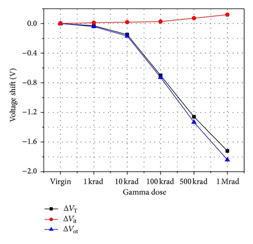
It can be observed from the figure that the interface charges shift the threshold voltage towards positive voltage, while the oxide charges cause the VT to shift towards more negative voltage. Since the oxide charge density is large compared to interface charge density, the voltage shift due to oxide trapped charges becomes dominating resulting in the total negative shift in the threshold voltage. The ΔVT for a MOSFET irradiated with 1 Mrad of gamma rays was found to be −1.72 V for which ΔVot contributes with −1.84 V and ΔVit contributes with 0.12 V. Similar results were observed for other gamma doses which are summarized in Table 2. The changes in oxide charge density (ΔNOT) and interface charge density (ΔNIT) are calculated from ΔVot and ΔVit. Figure 5 shows the variation in ΔNOT and ΔNIT for various gamma doses.
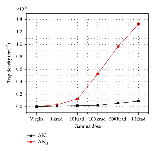
The ΔNOT and ΔNIT of 1 Mrad gamma irradiated P-channel MOSFETs were found to be 1.33 × 1012 cm−2 and 8.72 × 1010 cm−2. The calculated values of ΔNOT and ΔNIT for various doses of gamma rays are summarized in Table 2.
4. Conclusion
The gamma ray induced total dose effects on P-channel MOSFETs have resulted in various parametric changes like increase in threshold voltage, subthreshold swing, reduced transconductance, and drain saturation current. Increase in oxide and interface trap densities is found to be the main degradation mechanism of gamma irradiated transistors. From the preceding results, it is very clear that the oxide trapped charges have the major contribution towards threshold voltage shift and the net threshold voltage shift is negative. The measurements confirm the fact that gamma rays seriously degrade the device performance to a greater extent.


