A Generic Three-Sided Rearrangeable Switching Network for Polygonal FPGA Design
Abstract
We propose a new Polygonal Field Programmable Gate Array (PFPGA) that consists of many logic blocks interconnected by a generic three-stage three-sided rearrangeable polygonal switching network (PSN). The main component of this PSN consists of a polygonal switch block interconnected by crossbars. In comparing our PSN with a three-stage three-sided clique-based (Xilinx 4000-like FPGAs) (Palczewski; 1992) switching network of the same size and with the same number of switches, we find that the three-stage three-sided clique-based switching network is not rearrangeable. Also, the effects of the rearrangeable structure and the number of terminals on the network switch-efficiency are explored and a proper set of parameters is determined to minimize the number of switches. Moreover, we explore the effect of the PSN structure and granularity of cluster logic blocks on the switch efficiency of PFPGA. Experiments on benchmark circuits show that switches and speed performance are significantly improved. Based on experiment results, we can determine the parameters of PFPGA for the VLSI implementation.
1. Introduction
Field Programmable Gate Arrays (FPGA’s) [1, 2] are now widely used for the implementation of digital circuits and many commercial products. A typical symmetric FPGA, consisting of an array of logic blocks (Ls) that can be connected by general routing resources, is shown in Figure 1. The routing resources comprise segments of wires and two kinds of blocks, switch blocks (SBs), and connection blocks (CBs). Both the switch and connection blocks contain many programmable switches. The input and output pins of a logic block are connected to its surrounding connection blocks, which in turn are connected to the switch blocks. An arbitrary digital circuit is divided into several parts such that each part is realized by a logic block; then these logic blocks are interconnected by routing resources in an FPGA.
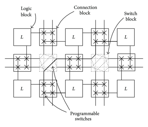
Since the programmable switches usually have high resistance and capacitance and occupy a large area, the number of programmable switches used in an FPGA affects its speed performance, die size, and routability. The time delay along an interconnection path is significant and often exceeds the delay of logic blocks. The routing area of FPGA typically takes from 70 to 90% of the total area [3]. Intuitively, increasing the number of programmable switches of routing network in an FPGA deliver good routability. However, routing network with fewer programmable switches can reduce the impedance of interconnecting paths, and the overall interconnecting speed of the FPGA can thus be improved.
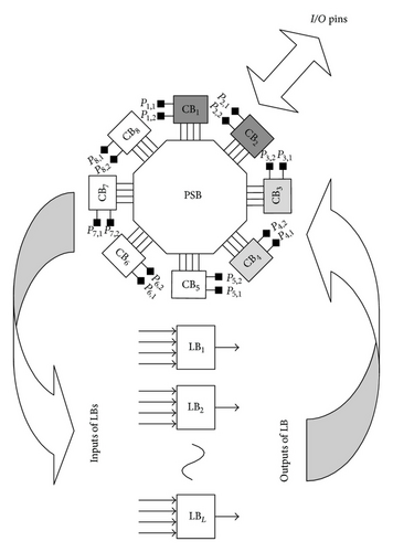
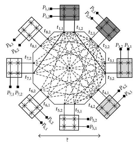
We propose a new Polygonal Field Programmable Gate Array (PFPGA) that consists of many logic blocks interconnect by a three-stage three-sided rearrangeable polygonal switching network. Figure 2 shows a model of polygonal FPGA, which consists of many clusters of logic block and I/O pins interconnected by a three-stage three-sided polygonal switching network. The polygonal switching network is a three-stage three-sided switching network for connecting inputs of logic-block (PI), outputs of logic-block (PO), and I/O pins (PP) to interconnect each other. A 3-sided switch network means that we have three disjoint sets (PP, PI, and PO) of terminals to be connected. Furthermore, in the 3-stage switching network, the longest connection of terminals is the length passing through 3 switches. Through the arrangement of switches (or interconnects) in various combinations, a terminal in one set can be connected to a terminal in any other set. Assuming that all connections are point-to-point connections, the enumeration of any pair of the above three sets of terminals to be connected is called an assignment, where a terminal of the three sets can appear in at most one pair. An assignment for a network is realizable if there exist in the network disjoint paths connecting every pair of terminals given in the assignment. A 3-sided switching network is rearrangeable [4–8] if any given assignment is realizable. Since a rearrangeable switching network has better capability to accomplish a given assignment, we focus on the design of a rearrangeable 3-sided switching network for the interconnection of terminals in a PFPGA.
Studies on multistage switching networks are fruitful. Yen and Feng [5] proposed a class of 2log 2 N-stage two-sided networks, which are equivalent to Benes networks. All networks in this class are nonblocking and rearrangeable. The one-stage one-sided rearrangeable switching networks have been discussed by Mitchell and Wild [6]; then, the reduction of crosspoints in the one-stage one-sided crosspoint switching network has been investigated by Varma and Chalasani [7]. Gordon and Srikanthan [8] studied another multistage one-sided switching network with many 2 × 2 switch elements. Chang et al. and Shyu et al. [9–11] proposed universal switch blocks that can improve the routability in a Xilinx 4000-like (clique-based) FPGAs routing network. Fan et al. [12] designed and proved a class of optimum Polygonal Switch Block PSB(m, S) for all even m and S ≥ 2. Yen et al. [13] proposed rearrangeable switch network that can improve the routability for a binary fat tree. However, most of the studies are concerned with either the two-sided rearrangeable switching networks or the one-stage one-sided rearrangeable switching networks. As well as, in terms of the number of switches, the one-sided or two-sided switching network is not efficient for interconnecting the three disjoint sets of terminals. Thus, this paper presents a generic three-stage three-sided rearrangeable switching network for Polygonal Field Programmable Gate Array by using Polygonal Switching Blocks (PSBs) [14–16] and crossbars. We investigate how to use PSBs to construct a rearrangeable 3-sided Polygonal switching network (PSN) and how to minimize the number of switches repaired. We also compare our PSN with a three-stage 3-sided clique-based (Xilinx 4000-like FPGAs) polygonal switching network of the same size and with the same number of switches and derive that the three-stage 3-sided clique-based polygonal switching network is not rearrangeable.
The next section gives a description on our polygonal FPGA model, 3-sided polygonal switching network, and some notations and definitions. In Section 3, we prove that our 3-sided switching polygonal network is rearrangeable, while Section 4 shows how we minimize the number of switches in a rearrangeable PSN. In Section 5, we propose a polygonal field programmable gate array that consists of many logic blocks interconnected by a PSN. Conclusions are reported in Section 6.
2. Polygonal Field Programmable Gate Array
Figure 2 shows a model of polygonal FPGA, which consists of many clusters of logic block and I/O pins interconnected by a generic three-sided Polygonal Switching Network. In this study, we investigate the logic block based on a cluster of 4-input look-up tables (LUTs). The reason is that most research has focused on LUT-based logic blocks, and Rose et al. [17] showed that a 4-input LUT is the most area-efficient LUT. The three-sided polygonal switching network consists of S connection blocks (CBs) and an S-sided polygonal switch block (PSB). Each connection block is connected to one of the S sides of the polygonal switch block. All the above blocks contain many programmable switches. The polygonal switching network is a three-stage three-sided switching network for connecting inputs of logic-block, outputs of logic-block, and I/O pins to interconnect each other. First, the input and output pins of cluster-based logic blocks and I/O pins are connected to the related connection blocks (CBs), which are then interconnected by a polygonal switch block. That is, the first and third stages consist of S CBs, and the second stage is a PSB with S sides. In this PFPGA, any two terminals of the three groups in a PFPGA can be connected with fewer than three switches. Thus, the speed performance of a PFPGA can be improved.
Since routing area in an FPGA is typically more than the active area, so we investigate how to use PSBs to construct a rearrangeable 3-sided Polygonal Switching Network (PSN) and how to minimize the number of switches repaired in the following section. We also compare our PSN with a three-stage 3-sided clique-based polygonal switching network of the same size and with the same number of switches and derive that the three-stage 3-sided clique-based polygonal switching network is not rearrangeable.
2.1. Three-Sided Polygonal Switching Network
The proposed generic three-stage 3-sided polygonal switching network (PSN) can be used to interconnect terminals in pairs of the three disjoint sets (PP, PO, and PI). This PSN consists of S crossbars (CBs) interconnected by a S-side polygonal switch block (PSB). Figure 3(a) shows an example of PSN, where the first and third stages are composed of 8 CBs; and the second (internal) stage is a PSB with 8 sides.
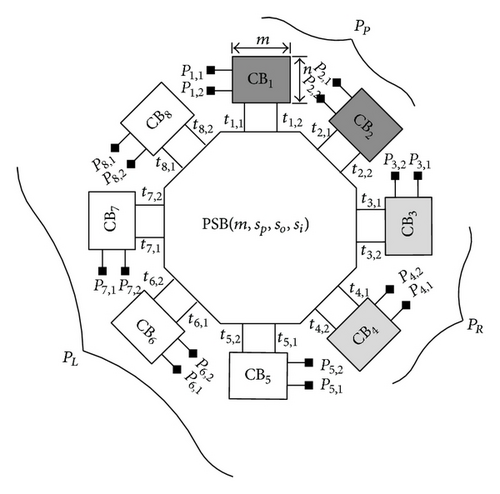
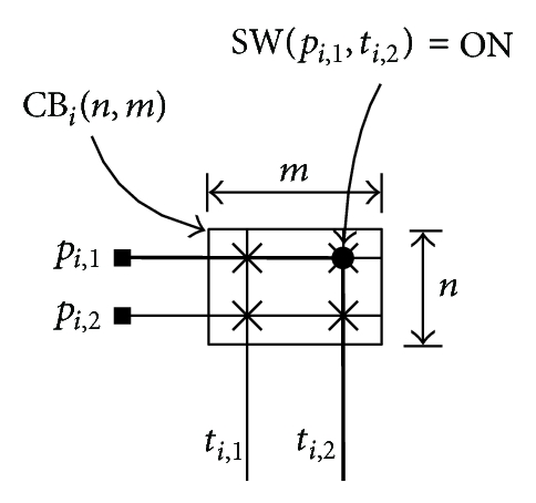
As shown in Figure 3(b), each crossbar in a PSN, denoted as CBi(n, m) for i = 1,2, …, S, is an n × m block architecture, where n is the number of external terminals connected to one of the three sets and m is the number of internal terminals connected to one side of PSB, m ∈ even [12]. We classify connection blocks CBs under three groups: CBI, CBO, and CBP, which are used to connect the inputs and outputs of logic-blocks and I/O pins, respectively. Denote that CBP = {CB1, CB2, …, , , , …, , , , …, , where sp, so, and si are the number of CBs in the CBP, CBO, and CBI, respectively. As shown in Figure 2, the I/O pins are connected to CBP = {CB1, CB2}, and inputs and outputs of logic-blocks are connected to CBI = {CB5, CB6, CB7, CB8} and CBO = {CB3, CB4}, respectively. Therefore, a three-sided polygonal switching network should provide NI = si × n, NO = so × n, and NP = sp × n external terminals to connect the inputs and outputs of logic-block and I/O pins, respectively.
We label these external and internal terminals on a CBi(n, m) as Pi = {pi,1, pi,2, …, pi,n} and Ti = {ti,1, ti,2, …, ti,m}, respectively. We represent the external terminals of a CBi(n, m)PP = (I/O terminals), PO = (output terminals), and PI = (input terminals). Similarly, the internal terminals are denoted as TP = , , and TI = . In total, we have two sets of terminals: the external terminal set 𝒫 = PP ∪ PO ∪ PI and the internal terminal set 𝒯 = TP ∪ TO ∪ TI in a PSN. Furthermore, the set of PP, PO, and PI have NP = sp × n, NO = so × n, and NI = si × n external terminals, respectively. Similarly, the set of TP, TO, and TI have MP = sp × m, MO = so × m, and MI = si × m internal terminals on S CB(n, m) crossbars. For example, Figure 3(a) shows a 3-sided switching network PSN with PP = P1 ∪ P2, PO = P3 ∪ P4, and PI = P5 ∪ P6 ∪ P7 ∪ P8, where Pi = {pi,1, pi,2}, i = 1, 2, …, 8; and with TP = T1 ∪ T2, TO = T3 ∪ T4, and TI = T5 ∪ T6 ∪ T7 ∪ T8, where Ti = {ti,1, ti,2}, i = 1, 2, …, 8. Any pair of external terminals from two sets of PP, PO, and PI can be connected to each other by using a 3-sided switching network PSN, but no pair external terminals from the same set can be interconnected.
Through the n × m programmable and electrically noninteracting switches in a crossbar CBi(n, m), every external terminal in Pi can be connected to a free internal terminal in Ti without any blocking. For example, if switch SW(pi,j, ti,h) is programmed to be “ON”, then connection (pi,j, ti,h) between an external terminal pi,j and an internal terminal ti,h is established, where 1 ≤ i ≤ S, 1 ≤ j ≤ n, and 1 ≤ h ≤ m. Figure 3(b) shows a routing example, where pi,1 is connected to ti,2 by programming SW(pi,1, ti,2), and this routing solution is illustrated by thick lines. In such a way, an external terminal can be connected to an internal terminal by programming one switch in a CBi(n, m).
The polygonal switch block in a PSN, denoted as a PSB(m, sp, so, si), is an S-side switch block with m internal terminals on each side of the block, as shown in Figures 4(a) and 5(a). Label the terminals on the ith side of a PSB(m, sp, so, si) as Ti = {ti,1, ti,2, …, ti,m} for 1 ≤ i ≤ S. Remember that internal terminals 𝒯 = TP ∪ TO ∪ TI, where , , and TI = . If a switch SW(ti,j, tk,l) exists in PSB(m, sp, so, si) and is programmed to be “ON”, then a connection between terminals ti,j and tk,l is established, where ti,j and tk,l belong to two different sets of TP, TO, and TI. To form a 3-sided switching network PSN we need S CB(n, m) crossbars connected to a polygonal switch block PSB(m, sp, so, si). Thus, a 3-sided switching network can be completely characterized by five parameters: n, m, sp, so, and si, and denoted as PSN(n, m, sp, so, si), for n ≥ 2, m ∈ even, sp ≥ 1, so ≥ 1, si ≥ 1, and S = sp + so + si. For example, Figure 3(a) shows a PSN with n = 2, m = 2, sp = 2, so = 2, and si = 4.
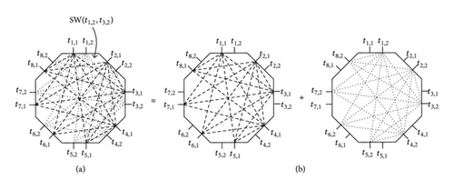
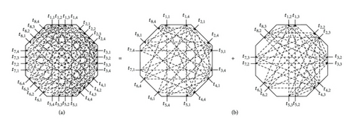
As shown in Figures 4(a) and 5(a), we will study the 3-sided switching network with two different topologies of polygonal switch blocks in this paper, denoted as PSBC(m, sp, so, si) and PSBSU(m, sp, so, si), respectively. Algorithm 1 constructs a clique-based polygonal switch block PSBC(m, sp, so, si). As shown in Figure 4, a PSBC(m, sp, so, si) is equivalent to m isolated PSBC(1, sp, so, si). In Figure 6 we show a 3-sided switching network, PSNC(n, m, sp, so, si) constructed with a PSBC(m, sp, so, si). Algorithm 2 constructs the polygonal switch block PSBSU(m, sp, so, si). As shown in Figure 5, a PSBSU(m, sp, so, si) is equivalent to m/2 isolated PSBSU(2, sp, so, si), m ∈ even. A 3-sided switching network PSNSU(n, m, sp, so, si) consisting of S CB(n, m) crossbars connected to a PSBSU(m, sp, so, si) is shown in Figure 7. Table 1 lists some symbols of 3-sided switching network specified in this paper.
| Symbol | Description |
|---|---|
| CB(n, m) | n × m crossbar |
| PSB(m, sp, so, si) | S-side PSB with m internal terminals, S = sp + so + si |
| PSBC(m, sp, so, si) | A clique-based PSB(m, sp, so, si) |
| PSBU(m, sp, so, si) | A universal PSB(m, sp, so, si) |
| PSBSU(m, sp, so, si) | A semiuniversal PSB(m, sp, so, si) |
| PSN(n, m, sp, so, si) | S CB(n, m)’s + PSB(m, sp, so, si) |
| PSNC(n, m, sp, so, si) | A PSN(n, m, sp, so, si) with PSBC |
| PSNU(n, m, sp, so, si) | A PSN(n, m, sp, so, si) with PSBU |
| PSNSU(n, m, sp, so, si) | A PSN(n, m, sp, so, si) with PSBSU |
| SWSU(n, m, sp, so, si) | The number of switches in a PSNSU(n, m, sp, so, si) |
-
Algorithm 1: Algorithm for constructing an S-sided clique-based switch block of size m.
-
Algorithm: Clique-based PSBC(m, sp, so, si, 𝒯, SW).
-
Input: S = si + so + sp—number of sides of the polygonal switch block; m—number of
-
terminals on each side of the polygonal switch block, m ∈ even.
-
Output: (𝒯, SW); 𝒯 = TP ∪ TO ∪ TI: set of terminals; SW: set of switches.
-
(1) Let internal terminals ,
-
and
-
,
-
where Ti = {ti,1, ti,2, …, ti,m} for 1 ≤ i ≤ S.
-
(2) SW ← ∅;
-
(3) for i = 1 to si do
-
(4) for k = si + 1 to S do
-
(5) for j = 1 to m do
-
(6) SW ← SW ∪ {(ti,j, tk,j)};
-
(7) for i = si + 1 to si + so do
-
(8) for k = si + so + 1 to S do
-
(9) for j = 1 to m do
-
(10) SW ← SW ∪ {(ti,j, tk,j)};
-
(11) Return (𝒯, SW)
-
Algorithm 2: Algorithm for constructing an S-sided semi-universal switch block of size m.
-
Algorithm: Semi-universal PSBSU(m, sp, so, si, 𝒯, SW).
-
Input: S = si + so + sp—number of sides of the polygonal switch block; m—number of
-
terminals on each side of the polygonal switch block, m ∈ even.
-
Output: (𝒯, SW); 𝒯 = TP ∪ TO ∪ TI: set of terminals; SW: set of switches.
-
(1) Let internal terminals ,
-
and
-
,
-
where Ti = {ti,1, ti,2, …, ti,m} for 1 ≤ i ≤ S.
-
(2) SW ← ∅;
-
(3) for i = 1 to sp do
-
(4) for k = sp + 1 to S do
-
(5) for j = 1 to m do
-
(6) SW ← SW ∪ {(ti,j, tk,m−j+1)};
-
(7) for i = sp + 1 to sp + so do
-
(8) for k = sp + so + 1 to sp + so + si do
-
(9) for j = 1 to m do
-
(10) SW ← SW ∪ {(ti,j, tk,m−j+1)};
-
(11) Return (𝒯, SW)
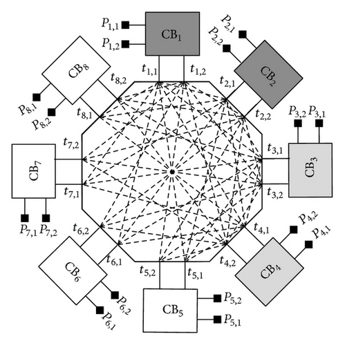
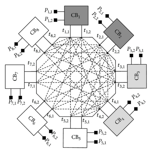
Note that we do not allow any two external terminals from the same set of PP, PO, and PI to be interconnected in a PSN(n, m, sp, so, si). Similarly, we do not allow any two internal terminals from the same set of TP, TO, and TI to be interconnected in a PSB(m, sp, so, si). For example, Figures 4(a) and 5(a) show that PSBC(2,2, 2,4) and PSBSU(4,2, 2,4) do not have any switches between the two sets of T1 and T2 from the same TP for the interconnection. That is, in either a PSNC(2,2, 2,2, 4) (Figure 6) or a PSNSU(2,2, 2,2, 4) (Figure 7) no interconnections of external terminals from the same sets of P1 and P2 through PSBC(2,2, 2,4) or PSBSU(2,2, 2,4) are allowed. In a PSBSU(m, sp, so, si) or PSBC(m, sp, so, si), since a terminal from a side in one set of TP, TO, and TI should be connected to any other terminal from the sides in the remaining two sets through switches, a polygonal switch block needs at least m(spso + spsi + sosi) switches. Assume that both 3-sided switching networks PSNSU(n, m, sp, so, si) and PSNC(n, m, sp, so, si) have the same size and the same number of switches. We will show that the three-stage 3-sided switching network PSNSU(n, m, sp, so, si) with m ≥ n is rearrangeable and m is even [12], but the PSNC(n, m, sp, so, si) with m = n is not rearrangeable.
In a PSN(n, m, sp, so, si), the connection pair (pi,j, pk,l) is a point-to-point connection, where pi,j and pk,l belong to different sets of PP, PO, and PI. An assignment AS = {(pi,j, pk,l)} represents a set of connection pairs to be connected; thus each external terminal appears in at most one pair. A PSN(n, m, sp, so, si) switching network is rearrangeable if any assignment AS is realizable (routable).
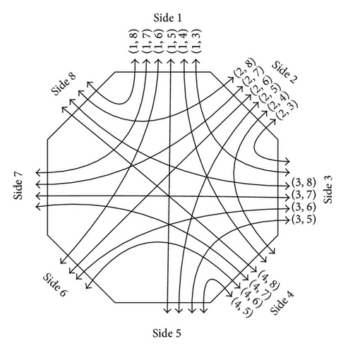
Note that a connection pair (pi,j, pk,l) belonging to AS is to be connected by passing through blocks CB − PSB − CB. Given an AS on a PSB(m, sp, so, si), each pair of connection is accomplished using terminals from two different sides of TP, TO, and TI; we can thus classify these connections passing through a PSB(m, sp, so, si) into (spso + spso + sosi) types of connections. Figure 8 shows the twenty possible types of connections in an eight-side switch block PSB(m, 2,2, 4). A routing requirement vector (RRV) [9–11] for a PSB(m, sp, so, si) is a (spso + spso + sosi)-tuple , , …, , …, , …, , …, , …, , where ri,k represents the number of type-(i, k) connections between Ti and Tk required to be connected through a PSB(m, sp, so, si); 0 ≤ ri,k ≤ m for 1 ≤ i < k ≤ S. In other words, ri,k is the number of connections {(pi,j, pk,l)} in AS to be connected through the two sides Ti and Tk on a PSB(m, sp, so, si), 1 ≤ j, l ≤ m, where Ti and Tk belong to any two different sets of TP, TO, and TI. An RRV is said to be realizable (routable) on a PSB(m, sp, so, si) if there exist disjoint paths for on a PSB(m, sp, so, si). Figure 8 shows an RRV = (r1,3, r1,4, r1,5, r1,6, r1,7, r1,8, r2,3, r2,4, r2,5, r2,6, r2,7, r2,8, r3,5, r3,6, r3,7, r3,8, r4,5, r4,6, r4,7, r4,8) for PSB with eight sides.
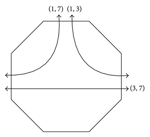
For example, Figure 9(a) shows a routing instance with three nets corresponding to the RRV = (11,3, 0, 0, 0, 11,7, 0, 0, 0, 0, 0, 0, 0, 0, 0, 13,7, 0, 0, 0, 0, 0), and we try to route this RRV using the two different polygonal switch blocks PSBC(2,2, 2,4) and PSBSU(2,2, 2,4) from Figures 4(a) and 5(b), respectively. As shown in Figures 9(b) and 9(c), however, there is always one net that cannot be routed on a PSBC(2,2, 2,4). Thus, this RRV (11,3, 0, 0, 0, 11,7, 0, 0, 0, 0, 0, 0, 0, 0, 0, 13,7, 0, 0, 0, 0, 0) is not routable on a PSBC(2,2, 2,4). Instances of the same RRV routable on a PSBSU(2,2, 2,4) are shown in Figures 10(a) and 10(b), where the routing solutions are illustrated by thick lines.
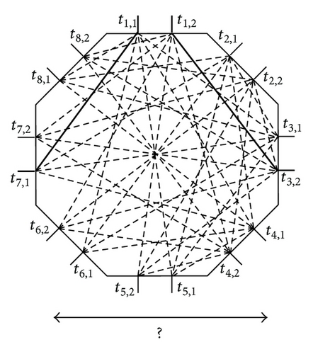
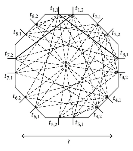
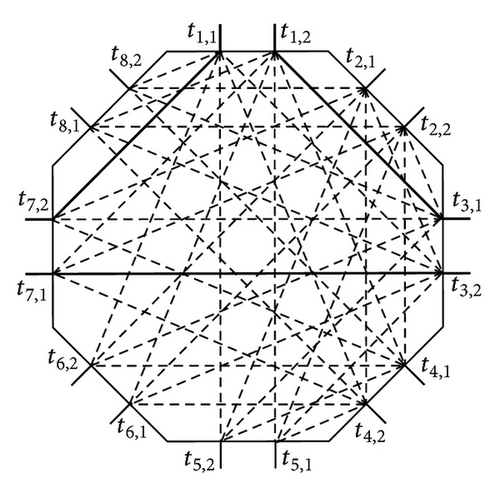
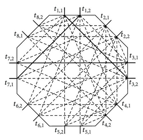
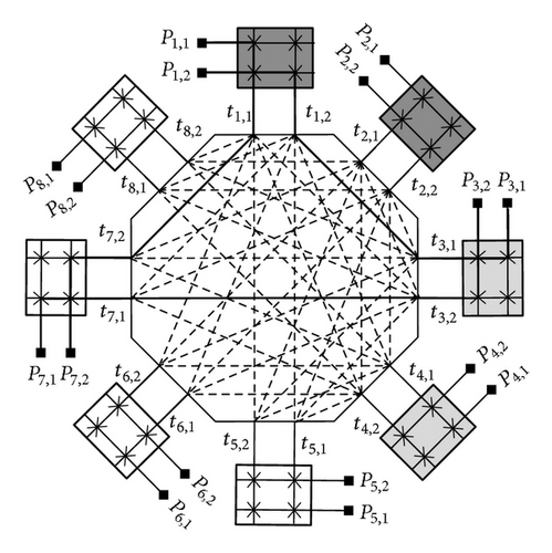
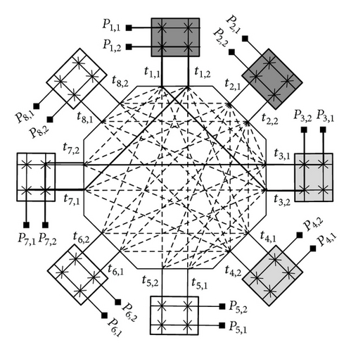
Each connection pair (pi,j, pk,l) ∈ AS is required to be connected by passing through CBi − PSB − CBk in a PSN(n, m, sp, so, si). Given an AS = {(pi,j, pk,l)}, we want to obtain an RRV , to be realized on a PSB(m, sp, so, si), where ri,k is the number of the connection pairs (pi,j, pk,l) required to be connected through PSB(m, sp, so, si). For example, let AS = {(p1,1, p7,2), (p1,2, p3,1), (p3,2, p7,1)} to be routed on a PSNC(2,2, 2,2, 4) and a PSNSU(2,2, 2,2, 4), which have been respectively shown in Figures 6 and 7. The RRV for the given AS on PSB(2,2, 2,4) is = (11,3, 0, 0, 0, 11,7, 0, 0, 0, 0, 0, 0, 0, 0, 0, 13,7, 0, 0, 0, 0, 0). We have already shown in Figures 10(a) or 10(b) that the RRV = (11,3, 0, 0, 0, 11,7, 0, 0, 0, 0, 0, 0, 0, 0, 0, 13,7, 0, 0, 0, 0, 0) can be routed on a PSBSU(2,2, 2,4). Since any external terminal in Pi can be connected to a free internal terminal in Ti without blocking through a crossbar CBi(n, m), we show in Figures 11(a) and 11(b) two possible routing solutions for the given AS on a PSNSU(2,2, 2,2, 4) switching network. Instances in Figures 12(a) and 12(b) show that the same AS is not routable on a PSNC(2,2, 2,2, 4) switching network, because the RRV = (11,3, 0, 0, 0, 11,7, 0, 0, 0, 0, 0, 0, 0, 0, 0, 13,7, 0, 0, 0, 0, 0) contains at least one connection that cannot be routed on a PSBC(2,2, 2,4) as already shown in Figures 9(b) and 9(c). Therefore, we conclude a PSNC(n, m, sp, so, si) switch network constructed with a PSBC(m, s), where m = n is not rearrangeable. In the following, we prove that a PSNC(n, m, sp, so, si) with m ≤ n is not rearrangeable.

Theorem 1. A 3-sided switching network PSNC(n, m, sp, so, si) is not rearrangeable for m ≤ n, m ∈ even, S = sp + so + si, sp ≥ 1, so ≥ 1, and si ≥ 1.
Proof. Observably, if a PSNC(n, m, sp, so, si) with m = n is not rearrangeable, then a PSNC(n, m, sp, so, si) with m < n is not rearrangeable. Thus, we need to prove that a PSNC(n, n, sp, so, si) is not rearrangeable.
Arbitrarily select three sides i, k, and u of a PSNC(n, n, sp, so, si), 1 ≤ i ≤ sp < k ≤ sp + so < u ≤ S, we form an assignment AS = {(pi,1, pu,1), (pi,2, pu,2), …, (pi,n−1, pu,n−1), (pi,n, pk,n), (pk,1, pu,n)} to be connected between the Pi ∈ PP, Pk ∈ PO, and Pu ∈ PI on a PSNC(n, n, sp, so, si). The RRV for routing ASD on a PSBC(n, sp, so, si) is , as shown in Figure 4(a). Since a PSBC(n, sp, so, si) is equivalent to n isolated PSBC(1, sp, so, si)’s, the first ri,u = (n − 1) can be realizable on (n − 1) isolated PSBC(1, sp, so, si)’s, as shown in Figure 4(b). But, we cannot find enough disjoint paths to simultaneously realize an ri,k = 1 and an rk,u = 1 on the last PSBC(1, sp, so, si), as shown in Figure 4(b). Thus, this AS cannot be realizable on a PSNC(n, n, sp, so, si), because this RRV contains at least one connection that cannot be routed on a PSBC(n, sp, so, si). Therefore, the PSNC(n, n, sp, so, si) is not rearrangeable.
In the following, we will explore the properties of the semiuniversal and polygonal switch block PSBSU(m, sp, so, si) and show a PSNSU(n, m, sp, so, si) switching network constructed with semiuniversal PSBSU(m, sp, so, si), where m ≥ n is rearrangeable.
2.2. Semiuniversal and Polygonal Switch Blocks
Note that the number of connections interconnecting through each side of PSB(m, S) cannot exceed m; this dimensional constraint [9–11] is characterized by the preceding S inequalities, one for each side.
Label the terminals on the ith side of a PSB(m, S) as Ti = {ti,1, ti,2, …, ti,m} for 1 ≤ i ≤ S. A generic universal switch block has been proposed by Shyu et al. [11]. As shown in Algorithm 3, the algorithm can be used to construct an S-side universal switch block PSBU(m, S) with m terminals on each side. That is to say, any RRV satisfying the dimension constraint (i.e., the number of connections on each side of a PSB(m, S) is at most m) is realizable on a PSBU(m, S), for S ≥ 2 and m ∈ even [12]. For example, Figure 13(b) shows a universal PSBU(2,6).
-
Algorithm 3: Algorithm for constructing an S-sided universal switch block of size m.
-
Algorithm: Universal switch block PSBU(m, S, 𝒯, SW).
-
Input: S = sp + so + si—number of sides of the polygonal switch block; m—number of
-
terminals on each side of the polygonal switch block, m ∈ even.
-
Output: (𝒯, SW); 𝒯: set of terminals; SW: set of switches.
-
(1) 𝒯 ← ti,j, ∀i = 1,2, …, S, ∀j = 1,2, …, m;
-
(2) SW ← ∅;
-
(3) for i = 1 to S − 1 do
-
(4) for k = i + 1 to S do
-
(5) for j = 1 to m do
-
(6) SW ← SW ∪ {(ti,j, tk,m−j+1)};
-
(7) Return (𝒯, SW)
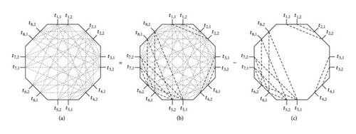
Since a semiuniversal PSBSU(m, sp, so, si) in a PSNSU(n, m, sp, so, si) does not allow any two internal terminals in the same set of TP, TO, and TI to be interconnected, where , , and , we have to modify Algorithm 3 to construct our PSBSU(m, sp, so, si). Algorithm 2 removes the switches SW(ti,j, tk,l), where ti,j and tk,l belong to the same set of TP, TO, and TI from PSBU(m, S), S = sp + so + si. For example, Figure 13(a) shows a semiuniversal switch block PSBSU(2,2, 2,4), which is equal to a universal PSBU(2,8) in Figure 13(b) minus some prohibited switches in Figure 13(c). That is to say, a semiuniversal switch block PSBSU(m, sp, so, si) contains a partial topology of the universal switch block PSBU(m, S).
Note that the number of connections interconnecting through each side of PSB(m, sp, so, si) cannot exceed m; this dimensional constraint is characterized by the preceding S inequalities, one for each side. Thus, the PSBSU(m, sp, so, si) constructed by Algorithm 2 is semiuniversal. Also, any RRV satisfying the dimension constraint is simultaneously realizable on a PSBSU(m, sp, so, si).
3. Rearrangeable 3-Sided Switching Networks
Since the programmable switches usually have high resistance and capacitance and occupy a large area, a rearrangeable 3-sided switching network PSN has routability and area efficiency. A 3-sided switching network PSNSU(n, m, sp, so, si) can be constructed with S CB(n, m) crossbars and a semiuniversal PSBSU(m, sp, so, si). Based on the semiuniversality of a PSBSU(m, sp, so, si) and the properties of a crossbar CB(n, m), we proceed to prove that the constructed PSNSU(n, m, sp, so, si) is rearrangeable.
Theorem 2. A 3-sided switching network PSNSU(n, m, sp, so, si) is rearrangeable if and only if m ≥ n, m ∈ even, S = sp + so + si, sp ≥ 1, so ≥ 1, and si ≥ 1.
Proof. Observably, if a PSNSU(n, m, sp, so, si) with m = n is rearrangeable, then a PSNSU(n, m, sp, so, si) with m ≥ n is rearrangeable. Thus, we need to prove that a PSNSU(n, n, sp, so, si) is rearrangeable, n ∈ even.
A PSNSU(n, n, sp, so, si) is used to connect the external terminals of PP, PO, and PI to each other. Let (I/O terminals), (output terminals), and (input terminals), where Pi = {pi,1, pi,2, …, pi,n} on a CBi(n, n), 1 ≤ i ≤ S. The connection pair (pi,j, pk,l) is a point-to-point connection, where pi,j and pk,l belong to different sets of PP, PO, and PI. An assignment AS = {(pi,j, pk,l)} represents a set of connection pairs to be connected; thus each external terminal appears in at most one pair. The PSNSU(n, n, sp, so, si) is rearrangeable if any assignment AS is realizable.
(If) Any assignment AS = {(pi,j, pk,l)} can be connected on PSNSU(n, n, sp, so, si), since each connection pair (pi,j, pk,l) ∈ AS is required to be connected by passing CBi—PSB—CBk, we can obtain that this kind of RRV , , …, , , …, , …, , …, , …, for any given AS to be realized on a PSNSU(n, sp, so, si), where ri,k represents the number of type-(i, k) connections between Pi and Pk. Furthermore, this RRV satisfying the dimension constraint is realizable on a semiuniversal PSBSU(n, sp, so, si), due to the number of connection pairs in AS interconnecting through each side of PSBSU(n, sp, so, si) does not exceed n. Therefore, for each (pi,j, pk,l) ∈ AS, we can find a connection path (ti,q, tk,n−q+1) between Ti and Tk after the RRV has been realized on a PSBSU(n, sp, so, si), where 1 ≤ q ≤ n. Then the connection (pi,j, pk,l) is realizable by programmed three switches, one switch SW(ti,q, tk,n−q+1) in the PSBSU(n, sp, so, si) and two other switches SW(pi,j, ti,q) and SW(pk,l, tk,n−q+1) in the CBi(n, n) and CBk(n, n), respectively. Therefore, any given assignment AS for a PSNSU(n, n, sp, so, si) is realizable, because there exist in the PSNSU(n, n, sp, so, si) disjoint paths connecting all the pairs of terminals given in the assignment AS. Thus, a PSNSU(n, m, sp, so, si) switching networks with m ≥ n is rearrangeable.
(Only if) If in a PSNSU(n, m, sp, so, si) with m < n, we have an assignment AS = {(pi,1, pk,1), (pi,2, pk,2), …, (pi,n, pk,n)} to be connected between the Pi and Pk on a PSNSU(n, m, sp, so, si), where Pi and Pk belong to different sets of PP, PO, and PI, since each connection pair (pi,j, pk,l) ∈ AS is connected by passing blocks CBi—PSB—CBk. In each CBi(n, m), we cannot find enough disjoint paths to connect all the n external terminals in Pi to all the m internal terminals in Ti, which in turn are connected to the ith side of a PSBSU(m, sp, so, si), due to m < n. Thus, this AS is not realizable on a PSNSU(n, m, sp, so, si) with m < n.
4. Minimize the Number of Switches
We have shown a rearrangeable 3-sided switching network PSNSU(n, n, sp, so, si) in the above section. Now, we start to explore the effect of the parameters sp, so, si, and n in a PSNSU(n, n, sp, so, si) on the switch-efficiency, and we try to find proper sp, so, si, and n values to minimize the number of switches needed in a rearrangeable PSNSU(n, n, sp, so, si) to interconnect terminal pairs from the three sets of PP, PO, and PI. We assume that the set of PP, PO, and PI have NP = sp × n, NO = so × n, and NI = si × n external terminals, respectively.
From (8), we have that a PSNSU(n, n, sp, so, si) with n = contains the number of switches to a minimum. Given a PSNSU(n, n, sp, so, si) interconnecting terminals pairs from PP, PO, and PI, where the set of PP, PO, and PI have NP, NO, and NI external terminals, respectively. Tables 2 and 3 show the number of switches needed in rearrangeable PSNSU(n, n, sp, so, si) each of which varies with n. In Table 2, the rearrangeable switching network PSNSU(8,8, 8,4, 16) with n = 8 (from (8)) is the best choice for interconnecting terminals pairs from the three terminal sets in terms of the number of switches. Furthermore, in Table 3, the rearrangeable switching network PSNSU(12,12,12,8, 16) with n = 11.7 (from (8)) is the best choice for interconnecting terminals pairs from the three terminal sets.
| PSNSU | SWSU(n, n, sp, so, si) | |||
|---|---|---|---|---|
| n | sp | so | si | |
| 2 | 32 | 16 | 64 | 7616 |
| 4 | 16 | 8 | 32 | 4480 |
| 8 | 8 | 4 | 16 | 3584 |
| 16 | 4 | 2 | 8 | 4480 |
| 32 | 2 | 1 | 4 | 7616 |
| PSNSU | SWSU(n, n, sp, so, si) | |||
|---|---|---|---|---|
| n | sp | so | si | |
| 2 | 72 | 48 | 96 | 30816 |
| 4 | 36 | 24 | 48 | 16704 |
| 6 | 24 | 16 | 32 | 12576 |
| 8 | 18 | 12 | 24 | 10944 |
| 12 | 12 | 8 | 16 | 10176 |
| 24 | 6 | 4 | 8 | 12864 |
| 48 | 3 | 2 | 4 | 21984 |
5. Polygonal FPGA
Figure 2 shows a model of polygonal FPGA (PFPGA), which consists of many clusters of logic block and I/O pins interconnected by a three-sided polygonal switching network. In this study, we investigate the logic block based on a cluster of 4-input look-up tables (LUTs). The three-sided polygonal switching network consists of S connection blocks (CBs) and an S-sided polygonal switch block (PSB). Each connection block is connected to one of the S sides of the polygonal switch block. All the above blocks contain many programmable switches. The polygonal switching network is a three-stage three-sided switching network [4] for connecting inputs of logic-block, outputs of logic-block, and I/O pins to interconnect each other. First, the input and output pins of cluster-based logic blocks and I/O pins are connected to the related connection blocks (CBs), which are then interconnected by a three-sided polygonal switch block (PSB). That is, the first and third stages consist of S CBs and the second stage is a PSB with S sides. In this PFPGA, any two terminals of the three groups in a PFPGA can be connected with fewer than three switches. Thus, the speed performance of a PFPGA can be improved.
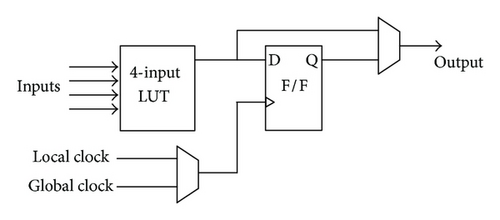
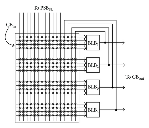
The key factors to the PFPGA switch-efficiency and speed-efficiency are the structure of its switching network PSNSU(n, m, sp, so, si) structure and the granularity of its cluster-based logic blocks CLB(k). That is to say, the parameters k and m in a PFPGA affect its speed performance, die size, and routability.
Cluster-based logic blocks have two other advantages over single BLB logic blocks. First, in an FPGA composed of logic clusters, many nets will be completely contained within a logic cluster. If these nets are routed using multiplexers within a cluster, the delay of these multiplexers is less than that of the main FPGA. Secondly, clustering k BLB’s into one logic cluster will greatly reduce the placement time by a factor of k, which is of increasing concern in today’s large FPGA’s.
5.1. Number of Switches in a PSNSU
Let L be the total number of BLB’s in a PFPGA with B I/O pins, and a BLB has r inputs and 1 output. The complete cluster-based logic block (CLB) is composed of k BLB’s, denoted as CLB(k). The number of switches in polygonal switching network PSNSU(n, m, sp, so, si) is obtained as follows.
- (i)
the number of switches in S CB(n, m)’s is equal to S × m × n,
- (ii)
the number of switches in a PSNSU(m, sp, so, si) is equal to m(spso + spsi + sosi), where n = rk, si = ⌈L/k⌉, so = ⌈L/n⌉, sp = ⌈B/n⌉, and S = si + so + sp, and L, B and r are constants.
From (10), SWSU(n, m, sp, so, si) is determined by the k and m values. In the following section, we will find proper k values and m to minimize the number of switches needed in a polygonal switching network through experiments.
5.2. Experimental Results
To explore the effects of k and m values of a polygonal switching network on the switch-efficiency in a PFPGA with L BLB’s and B I/O pins, we have implemented a maze router [19–21] in C language and executed the codes on an IBM System M3. We examine the effect of two parameters, k and m, on the switch performance using the CGE [1] and SEGA [22] benchmark circuits.
By routing different cluster size of logic blocks, the switch performance of a three-sided polygonal switching network was evaluated. From the results of a CLB(5), as listed in Table 4, we first determine the minimum number of tracks m required to complete the 100% routing of each circuit, using three-sided polygonal switching networks PSNSU(n, m, sp, so, si). Then we can find the SWSU(n, m, sp, so, si) value by substituting the values of n, m, si, so, and sp into (10).
| Circuit | LBs | #Con. | PSNSU(n, m, si, so, sp) | ||||
|---|---|---|---|---|---|---|---|
| m | si | so | sp | SWSU | |||
| BUSC | 24 × 22 | 392 | 22 | 22 | 6 | 4 | 9064 |
| DMA | 34 × 30 | 771 | 24 | 45 | 11 | 2 | 14358 |
| DFSM | 44 × 42 | 1422 | 27 | 84 | 20 | 3 | 30690 |
| BNRE | 42 × 40 | 1257 | 27 | 76 | 19 | 4 | 29517 |
| Z03 | 52 × 50 | 2135 | 27 | 120 | 29 | 3 | 42894 |
| 9symml | 20 × 18 | 259 | 22 | 15 | 4 | 1 | 4428 |
| alu2 | 28 × 24 | 511 | 23 | 29 | 7 | 1 | 8007 |
| alu4 | 36 × 32 | 851 | 27 | 51 | 13 | 2 | 17235 |
| apex7 | 22 × 18 | 300 | 22 | 16 | 4 | 5 | 7988 |
| example2 | 26 × 22 | 444 | 23 | 24 | 6 | 8 | 13122 |
| k2 | 42 × 38 | 1256 | 25 | 72 | 18 | 5 | 28050 |
| term1 | 18 × 16 | 202 | 22 | 12 | 3 | 3 | 5100 |
| too_large | 28 × 26 | 519 | 22 | 32 | 8 | 3 | 11004 |
| vda | 32 × 30 | 722 | 25 | 42 | 10 | 3 | 14750 |
| Total | — | — | — | — | — | — | 236207 |
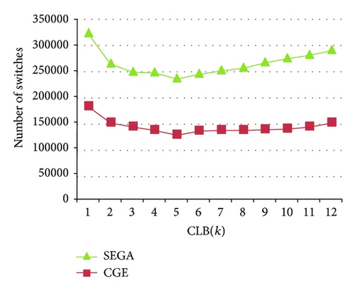
Figure 16 shows that the numbers of programmable switches SWSU(n, m, sp, so, si) used in the 14 benchmarks vary with CLB(k), where k = 1,2, …, 12. Experimental results demonstrate that the switches number used in PSNSU is minimum for a PFPGA with CLB(5) (for CGE) and CLB(3) (for SEGA), respectively. We assume that the available pin count of a PFPGA is B = 84 and the number of BLB is about 208. Therefore, our PFPGA consists of 52 CLB(5) and B = 84 I/O pins interconnected by a three-sided polygonal switching network SWSU(n = 20, m = 25, si = 52, so = 11, sp = 5).
5.3. VLSI Chip Implementation of the PFPGA
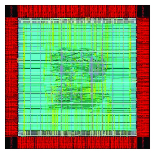
The chip layout of our PFPGA using a 0.18 μm CMOS technology is shown in Figure 17. The polygonal switching network area of a PFPGA is 1255 μm × 1350 μm. And the total area of this PFPGA is 1550 μm × 1600 μm. So we can calculate the ratio of routing area to total area to be 68.81%. Since routing area typically takes 70–90 percent of the total chip area in general FPGA [3]. So we conclude that the polygonal FPGA gets more area utilization.
In our proposed PFPGA architecture, we provide a three-stage routing resources concept. The first and third stages of routing are the connection blocks in two CLBs, which can meet local signal routing requirements. And the second layer of routing is the polygonal switch block, which is used to connect any output signal of a CLB to any input signal of a CLB. Thus, the longest distance in our PFPGA is only three stages. The maximum point-to-point of PSNSU delay is 13 ns. So we conclude that the architecture of PFPGA has better speed improvement. As mentioned above, this chip architecture uses less number of programmable switches and the speed performance of a PFPGA can be achieved. Thus, it is very suitable for VLSI implementation.
6. Conclusions
This paper first proposed a generic three-stage and rearrangeable three-sided switching network PSNSU(n, m, sp, so, si) used in the PFPGA for all even m. The PSN consists of S CB(n, m) crossbars interconnected by a semiuniversal polygonal switch block PSNSU(m, sp, so, si) with S sides. We not only provide the designers with a rearrangeable PSNSU(n, m, sp, so, si) with m ≥ n for connecting terminal pairs from three disjoint terminal sets to each other but also determinate the important parameter n to minimize the number of switches needed in that network. We also propose a PFPGA that consists of many logic blocks interconnected by a PSNSU. We investigate the effect of the PSNSU structure and the granularity of its interconnecting cluster-based logic blocks on the switch-efficiency and speed-efficiency performance. Experimental results demonstrate that the switch-efficiency and speed-efficiency are improved so it holds promise as a practical PFPGA with polygonal switching network.
Acknowledgment
This work was partly supported by the National Science Council, Taiwan, under Grant NSC 101-2221-E-019-071.


