Silicon Nitride Film by Inline PECVD for Black Silicon Solar Cells
Abstract
The passivation process is of significant importance to produce high-efficiency black silicon solar cell due to its unique microstructure. The black silicon has been produced by plasma immersion ion implantation (PIII) process. And the Silicon nitride films were deposited by inline plasma-enhanced chemical vapor deposition (PECVD) to be used as the passivation layer for black silicon solar cell. The microstructure and physical properties of silicon nitride films were characterized by scanning electron microscope (SEM), Fourier transform infrared spectroscopy (FTIR), spectroscopic ellipsometry, and the microwave photoconductance decay (μ-PCD) method. With optimizing the PECVD parameters, the conversion efficiency of black silicon solar cell can reach as high as 16.25%.
1. Introduction
Black silicon is an effective method to reduce the surface reflectivity for optoelectronic devices and solar cells application. Many black silicon methods have been developed, including reactive ion etching [1], metal-assisted chemical etching [2], and irradiating the silicon surface with femtosecond laser pulses [3]. In our previous study [4, 5], plasma immersion ion implantation (PIII) process has been put forward to produce black silicon with advantages of low cost and high throughput. During the PIII process, the reactive ions are injected into the silicon lattice and react with silicon, and then black silicon with various microstructures can be formed. Although the black silicon has very low surface reflectivity, the conversion efficiency can not be improved significantly when the black silicon is used for solar cells application. In order to produce high-efficiency black silicon solar cell, the matching process (e.g., Phosphorus diffusion process, PECVD SiNx film process, and cofiring process) should be improved. Due to the unique microstructure of the black silicon, the passivation process is of significant importance to produce high-efficiency solar cell. PECVD SiNx film is widely used in photovoltaic industry, which cannot only be used as antireflective coating (ARC) but also provide surface passivation effect and excellent bulk passivation for multicrystalline silicon solar cell due to a large amount of hydrogen originating from plasma gas dissociation and incorporated in the SiNx film [6].
In the present study, PECVD SiNx film is used to passivate the black silicon for solar cells. A detailed study on the physical properties of the as-grown SiNx films as functions of the PECVD parameters will be carried out. The passivation effects of the SiNx film on the black silicon solar cell will also be discussed.
2. Experimental Details
The material used for experiments was commercially available boron-doped p-type multicrystalline silicon wafers obtained from the ingot by wire sawing of thickness ~200 μm, area 156 mm × 156 mm, and resistivity 1~3 Ω cm. Damage on the surface induced by wire cutting was removed by etching in 10% NaOH solution at 80°C. The black silicon was prepared by plasma immersion ion implantation process on home-made equipment and subsequently subjected to acid etching in 2% HCl and then in 10% HF to remove the contamination and oxides. After that, the black silicon wafers were phosphorus doped using phosphorous oxychloride (POCl3) as the dopant source and then subjected to edge etching through reactive ion etching and removing phosphosilicate glass (PSG) layer with diluted HF (10% by volume). Silicon nitride film for passivation was grown by PECVD process with different gas flow ratios of NH3/SiH4, deposition time and deposition temperatures. Finally, the front and back metallization of all the black silicon wafers was carried out by screen-printing technique and followed by baking and cofiring in a conveyer belt furnace.
The structure and physical properties of silicon nitride were characterized by scanning electron microscope (SEM), Fourier transform infrared spectroscopy (FTIR), spectroscopic ellipsometry, and the microwave photoconductance decay (μ-PCD) method. The surface reflectance was examined by a UV-VIS-NIR spectrophotometer (Varian Cary 5000) equipped with an integrating sphere detector in the wavelength from 300 to 1100 nm. I-V characterization was used to evaluate the black silicon solar cell under one sun global solar spectrum of AM 1.5 at 25°C.
3. Results and Discussion
3.1. The Microstructure of Black Silicon
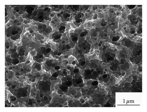
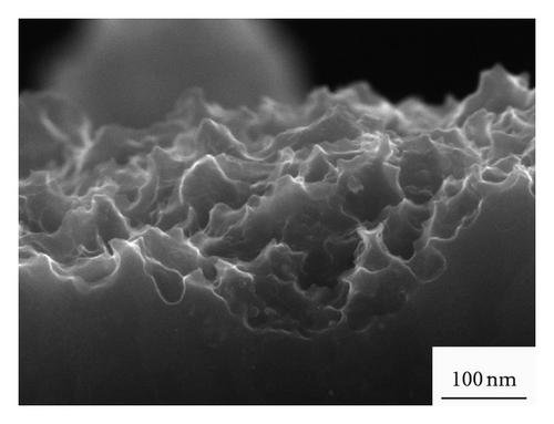
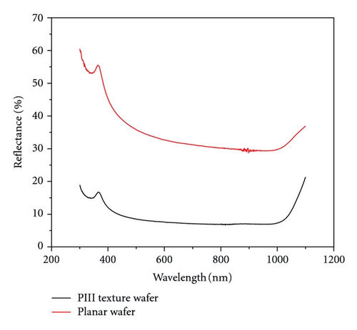
The microstructure of the black silicon produced by PIII is shown in Figure 1. The surface of the black silicon appears to be porous sponge like microstructure. The evaluated dimension of randomly distributed structures is less than 1 μm (varied from 100 nm to 300 nm). Due to such morphology, a reduced effective reflectance value about 7% in the wavelength from 300 nm~1100 nm is obtained, presented in Figure 2.
3.2. Gas Flow Ratio
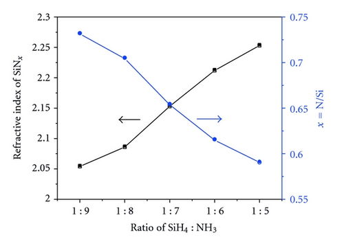
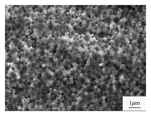
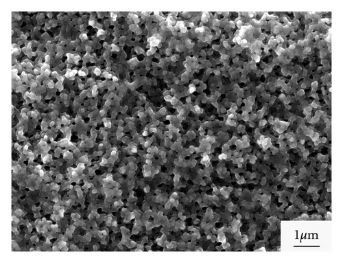
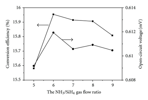
Figure 5 shows the conversion efficiency and open-circuit voltage of the black silicon solar cell varying with the NH3/SiH4 gas flow ratio. The conversion efficiency and open-circuit voltage reach their highest value when the NH3/SiH4 gas flow ratio is 6, indicating that the SiNx film has a good passivation effect on black silicon when the NH3/SiH4 gas flow ratio is 6.
3.3. Deposition Temperature
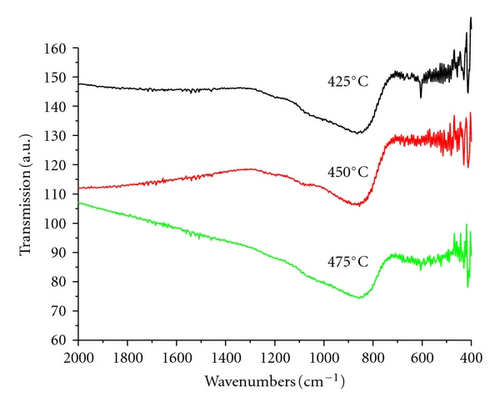
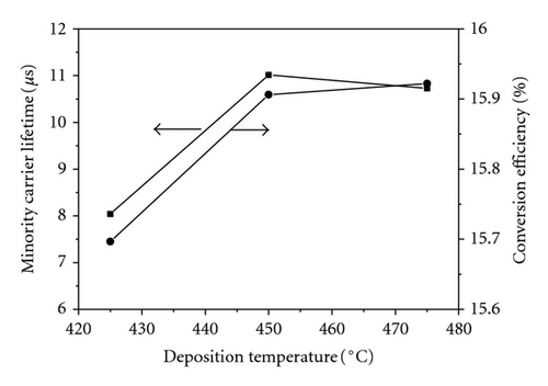
Deposition temperature is also a crucial parameter to determine the passivation effect for black silicon in the process of PECVD SiNx film. Keeping the deposition time at 500 s, deposition power at 3000 W and the NH3/SiH4 gas flow ratio at 6, the deposition temperature is varied from 425°C to 475°C. Figure 6 shows the FTIR transmission spectra of the SiNx films grown at 425°C, 450°C, and 475°C, respectively. All the spectra show a strong absorption band centered at approximately 840–890 cm−1 that can be identified with the asymmetric stretching mode of vibration of the Si–N bond. This band shifts very slightly varying with the deposition temperature, indicating that the deposition temperature affects the chemical composition very slightly. Figure 7 shows the minority carrier lifetime and conversion efficiency of the black silicon after PECVD the SiNx films at 425°C, 450°C, and 475°C, respectively. Higher deposition temperature will result in higher minority carrier lifetime and conversion efficiency. It is believed that relatively high deposition temperature facilitates hydrogen atoms diffuse into silicon substrate and consequently reduces the recombination center, contributing to an increase of conversion efficiency. Considering equipment factor, 450°C is preferable deposition temperature.
3.4. Deposition Time
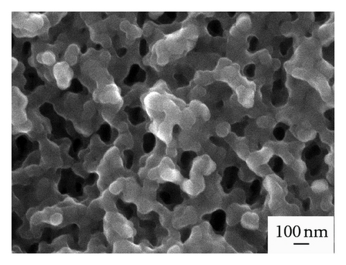
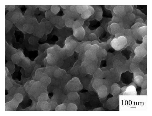
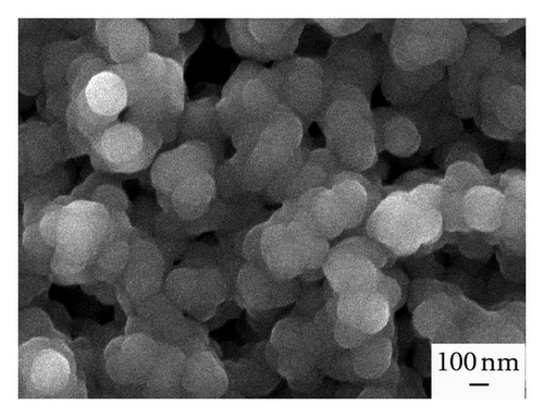
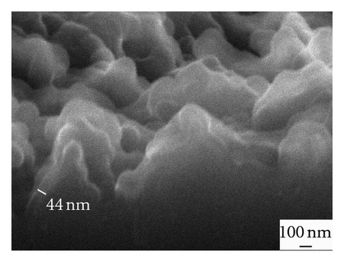
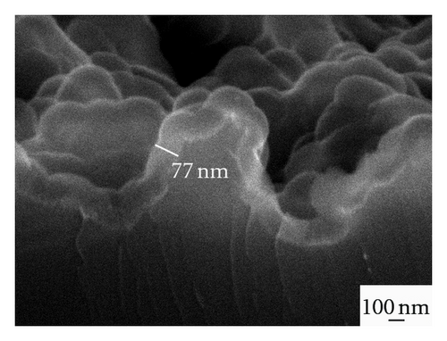
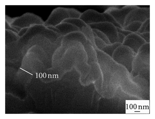
Figure 8 shows the microstructure of the SiNx films varying with deposition time. It can be seen that the SiNx film becomes denser, and the thickness increases with the deposition time. Also it can be obviously seen that the SiNx film has a good coverage on black silicon surface, and the thickness is more uniform when the deposition time is 500 s. Table 1 shows the influence of deposition time on the properties of black silicon solar cells. The open circuit voltage gradually increases varying with deposition time from 300 s to 700 s. The increase of Voc can be attributed to the improvement of passivation. As increasing the deposition time, more hydrogen atoms are diffused into silicon bulk to passivate defects and dislocation, leading to a decrease of recombination center. It can also be seen that the series resistance increases with increasing the deposition time. This is due to that, with increasing the thickness of SiNx film, Ag paste is hard to fire through thick SiNx film.
| Voc (V) | Isc (A) | Rs (mΩ) | Eff (%) | |
|---|---|---|---|---|
| 300 | 0.605 | 8.01 | 3.19 | 15.23 |
| 500 | 0.611 | 8.25 | 3.21 | 15.91 |
| 700 | 0.613 | 8.22 | 4.62 | 15.66 |
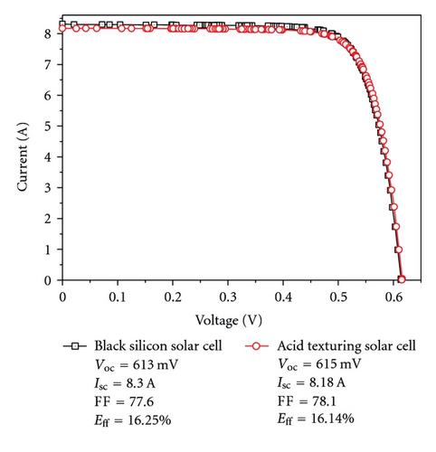
With optimizing the PECVD parameters (the NH3/SiH4 gas flow ratio : 6, deposition temperature : 450°C, and deposition time : 500 s), the conversion efficiency of the black silicon solar cell can reach as high as 16.25%. The current-voltage (I-V) characteristics of black silicon solar cells compared with acid-textured Si solar cell are shown in Figure 9.
4. Conclusion
The black silicon has been produced by plasma immersion ion implantation (PIII), and its surface appears to be porous sponge like microstructure. To passivate the black silicon, SiNx film was deposited by inline PECVD using ammonia and silane as the reactant gas. The black silicon solar cell is high when the NH3/SiH4 gas flow ratio is 6, the deposition temperature is 450°C, and the deposition time is 500 s. With optimizing these parameters, the conversion efficiency of black silicon solar cell reaches as high as 16.25%. This work constitutes the most important step to optimize the SiNx film, which allows us to design a desirable film for black silicon solar cell. Matched by adequate metallization step, the conversion efficiency of the black silicon solar cell can be further improved.
Acknowledgment
This work was supported by the National Natural Science Foundation of China (no. 61106060) and the Instrument Developing Project of the Chinese Academy Sciences (no. YZ200755).


