PV Power-Generation System with a Phase-Shift PWM Technique for High Step-Up Voltage Applications
Abstract
A PV power-generation system with a phase-shift pulse-width modulation (PWM) technique for high step-up voltage applications is proposed. The proposed power-generation system consists of two stages. In the input stage, all power switches of the full-bridge converter with phase-shift technique can be operated with zero-current switching (ZCS) at turn-on or turn-off transition. Hence, the switching losses of the power switches can be reduced. Then, in the DC output stage, a voltage-doubler circuit is used to boost a high dc-link bus voltage. To supply a utility power, a dc/ac inverter is connected to induce a sinusoidal source. In order to draw a maximum power from PV arrays source, a microcontroller is incorporated with the perturbation and observation method to implement maximum power point tracking (MPPT) algorithm and power regulating scheme. In this study, a full load power of 300 W prototype has been built. Experimental results are presented to verify the performance and feasibility of the proposed PV power-generation system.
1. Introduction
To overcome fossil energy shortage and reduce air pollution, the demand of renewable energy sources has been increased significantly. One of these sources is PV arrays energy, which is clean, quiet, and maintenance-free [1, 2]. In practice, the output voltage level of PV arrays is usually much lower than that of high dc-link bus voltage. This means that a front-end dc/dc converter is required to boost the low voltage of the PV arrays to a standard high dc-link bus voltage before being inverted into a 110 Vac (or 220 Vac) output. Thus, the dc/dc converter with a high step-up voltage ratio and high efficiency is usually demanded. Furthermore, to obtain maximum power from PV modules, tracking the maximum power point (MPP) of PV arrays is also an essential part of the PV power system, which is mostly realized by a microcontroller with a perturbation and observation method [3–5].
To achieve a high step-up voltage ratio, high efficiency, and galvanic isolation, a voltage-fed phase-shift full-bridge converter is used as a common solution [6–11]. However, it has several disadvantages, such as large input current ripple, large circulation current and high conduction losses of power switches. Compared with the voltage-fed phase-shift full-bridge converter, the current-fed phase-shift full-bridge converter has the clear advantages of lower input-current-ripple and less conduction losses of power switches in the low-input high-output voltage conversion system. In this paper, a PV power-generation system with a current-fed phase-shift full-bridge converter for high step-up voltage applications is proposed, as shown in Figure 1. The proposed PV power-generation system has features as follows. (1) MPPT feature can be realized by a microcontroller with perturbation and observation method. (2) DC power from the PV arrays can induce a utility power via a dc/ac inverter. (3) Zero-current switching (ZCS) technology is implemented for all power switches (4) Electricity isolation is naturally obtained.
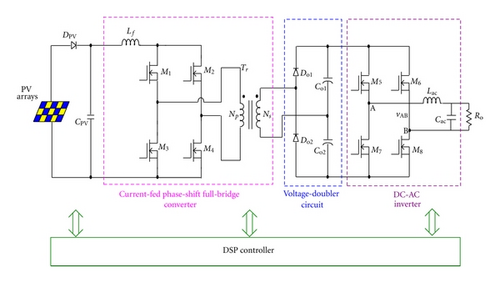
The operational principle of the proposed PV power-generation system is described in Section 2. The MPPT control scheme and protection circuit of the proposed PV power-generation system are described in Section 3. The design considerations of key components are described in Section 4. Experimental results obtained from a 300 W prototype with the proposed power-generation system for PV arrays source are presented in Section 5. Finally, a conclusion is given in Section 6.
2. Operational Principle
The circuit structure of the proposed PV power system is shown in Figure 1, in which it is composed of a current-fed phase-shift full-bridge converter, a voltage-doubler circuit and a dc-ac inverter in cascade connection. By adopting a digital signal processor (DSP) control scheme with the perturbation and observation method [12–16], the proposed PV power system can draw power from the PV arrays source with MPPT features, and feed the drawn power to the voltage-doubler circuit. Then, the dc-ac inverter operated with sinusoidal pulse-width modulation (SPWM) control scheme will generate a utility power [17–20]. For convenience of illustration and analysis, the proposed PV power-generation system shown in Figure 1 is redrawn in Figure 2.
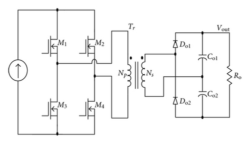
- (1)
Boost inductor Lf is large enough so that the current flowing through it is constant over a switching period.
- (2)
All of the switching devices and components are ideal.
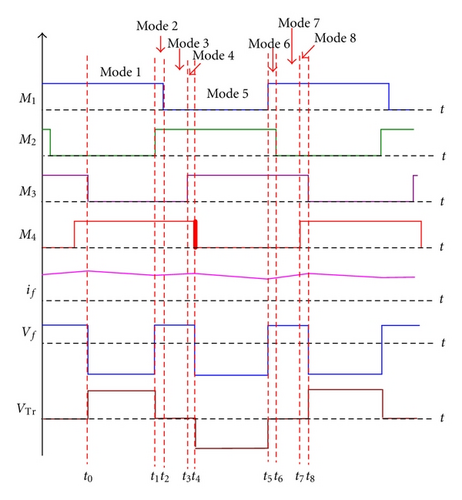
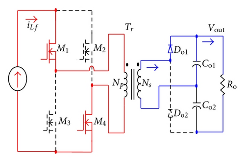
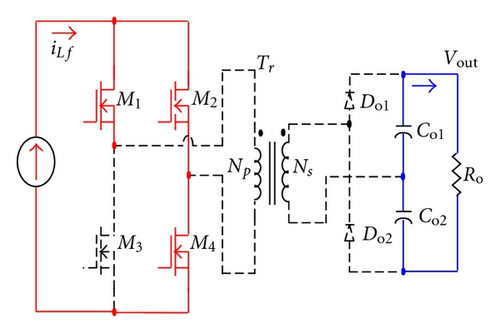
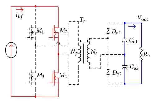
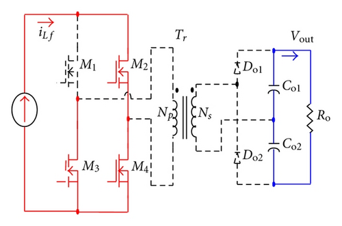

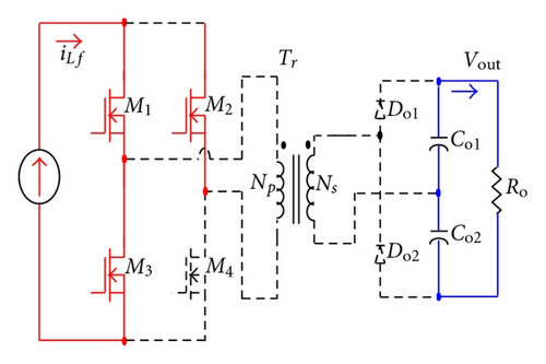
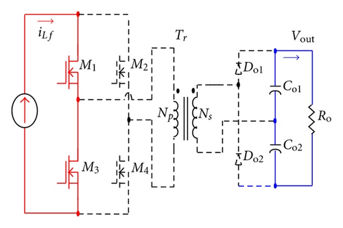
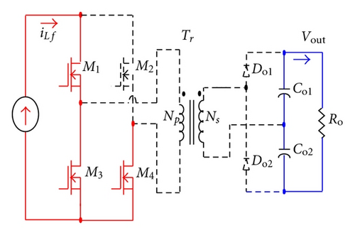
Based on the above assumptions, the operational principle can be explained mode by mode as follows:
Mode 1 (Figure 4(a), t0 ≤ t < t1). This mode begins when power switches M1 and M4 are turned on at time t0, and input current if starts to flow from the PV arrays through the transformer primary winding. At this operation, there will be a voltage across the secondary winding, which will turn on Do1. Then, the current in the secondary winding will flow through Co1 and the load. The equivalent circuit of Mode 1 is shown in Figure 4(a).
Mode 2 (Figure 4(b), t1 ≤ t < t2). At time instant t1, M2 is turned on and M1 as well as M4 are still kept on but no current flows through M1. The input current if is free-wheeling through power switches M2 and M4 and no current will flow through the transformer windings. Diodes Do1 and Do2 in secondary side of the transformer will be turned off, since all of transformer winding voltages are clamped to zero. The equivalent circuit of Mode 2 is shown in Figure 4(b).
Mode 3 (Figure 4(c), t2 ≤ t < t3). At time instant t2, power switch M1 is turned off at zero current due to the reason that there is no conducted current in the previous operating stage. That is, M1 is operated with ZCS at turn-off transition. The power switches M2 and M4 are maintained on, and input current if is continuous free-wheeling through M2 and M4. The equivalent circuit of Mode 3 is shown in Figure 4(c).
Mode 4 (Figure 4(d), t3 ≤ t < t4). At time instant t3, power switches M2 and M4 are still kept on. Power switch M3 is turned on and operated with ZCS at turn-on transition, because transformer winding has no voltage. The equivalent circuit of Mode 4 is shown in Figure 4(d).
Mode 5 (Figure 4(e), t4 ≤ t < t5). At time instant t4, power switches M2 and M3 are still kept on and M4 is turned off. The input current is starts to revise flowing through the transformer primary winding. At this operation, there will be a revised voltage across the secondary winding of transformer which will turn on Do2. Thus, the current in the secondary winding will flow through Co2 and the load. The equivalent circuit of Mode 5 is shown in Figure 4(e).
Mode 6 (Figure 4(f), t5 ≤ t < t6). At time instant t5, M2 and M3 are still kept on and M1 is turned on. The input current if is free-wheeling through power switches M1 and M3 and no current will flow through the transformer windings. Diodes Do1 and Do2 in the transformer secondary will be turned off once again, since all of transformer winding voltages are clamped to zero. The equivalent circuit of Mode 6 is shown in Figure 4(f).
Mode 7 (Figure 4(g), t6 ≤ t < t7). At time instant t6, M1 and M3 are still kept on and M2 is turned off. Power switch M2 is turned off under ZCS condition, due to the reason that there is no conducted current in the previous operating stage. The equivalent circuit of Mode 7 is shown in Figure 4(g).
Mode 8 (Figure 4(h), t7 ≤ t < t8). At time instant t7, M1 and M3 are still kept on and M4 is turned on and operated with ZCS at turn-on transition, because transformer winding has no voltage. The equivalent circuit of Mode 8 is shown in Figure 4(h). The proposed power system operation over one switching cycle is completed.
3. Control Scheme of MPPT
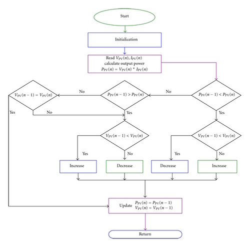
The PV arrays are constructed by many series or parallel connected solar cells. Each solar cell is formed by a P-N junction semiconductor, which can produce currents by the photovoltaic effect. The typical V-I and output power characteristic curves of the PV arrays with different insolations are shown in Figure 5. For a specific isolation, there exists one operating point where the PV array can generate its maximum output power. In order to achieve the best energy utilization of the PV arrays, an MPPT algorithm must be integrated into the control strategy of the current-mode phase-shift full-bridge converter.
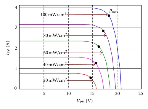
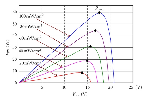

In order to regulate the output voltage of the proposed PV power-generation system and provide high-quality ac power to the load, the effective voltage and current feedback compensators are essential. By processing of feedback compensators, the voltage error signal ve1 and current error signal ie1 will be obtained. Then, the PWM1 compensator will generate driving signals of switches (M1 ~ M4) to regulate the dc output voltage. The output voltage of inverter vac and its filter inductor current iac are sampled to generate driving signals of switches (M5 ~ M8) and employed to realize a high steady and dynamic response sinusoidal voltage. The control strategies can be implemented by the TMS320F240 microcontroller to improve the system performance. The conceptual control block diagram of the proposed PV power-generation system is shown in Figure 8.
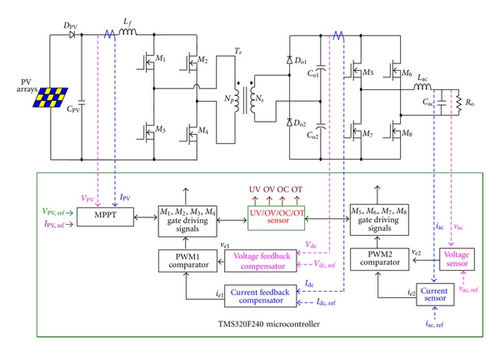
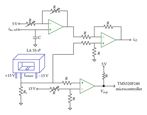
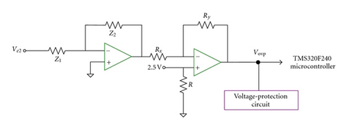
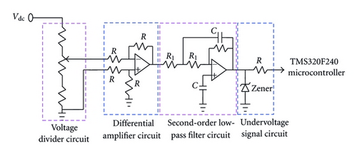
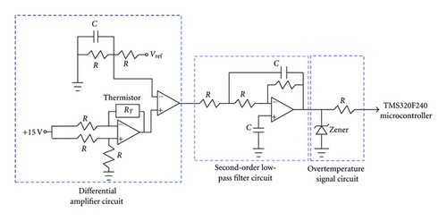
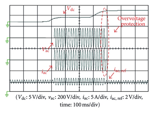
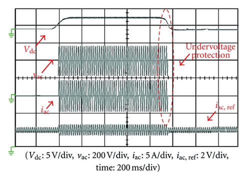
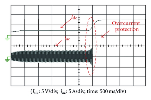
To achieve an optimal stability and safety for the proposed PV power-generation system, the functions of undervoltage, overvoltage protection, overcurrent protection, and overtemperature protection are required. Figures 9 and 10 show the key protection circuits of the proposed PV power-generation system. All of the protection signals are also realized on the TMS320F240 microcontroller, as shown in Figure 8.
4. Design Considerations of Power Switches
Most power converters have power components that operate at temperatures that are high enough to cause burns if handled improperly. The power dissipation in power switches normally increases with the internal temperature, and the losses become excessively high even at temperatures of 200°C. Component manufacturers typically will guarantee the maximum values of component parameters such as onstate conduction voltages, switching frequencies, and switching losses at a specified maximum temperature, which varies from one type of component to another and is often at 125°C. Therefore, a system intended to have high reliability would be designed for a worse-case junction temperature in power switches of 20–40°C below 125°C. In order to reduce temperatures of the power switches for the proposed PV power-generation system, the small heat sinks are usually recommended.
The proposed PV power-generation system consists of a phase-shift full-bridge converter, a voltage-doubler circuit, and a full-bridge inverter, as shown in Figure 1. To design the proposed PV power-generation system, their power switches are considered in the following.
4.1. Selection of the Power Switches (M1 ~ M4)
For the current-fed full-bridge phase-shift converter, the voltage stress imposed on power switches (M1 ~ M4) is Vds(max ) = VPV + VLf = 40 V. When power switches are turned on, the maximum switching current ids(peak) is equal to the current iLf(peak). Thus, the maximum switching current ids(peak) = 10 A. Selection of power switches involves a tradeoff between conduction losses and switching losses. MOSFETs with low Rds(on ) can usually keep low conduction losses and temperatures, but they usually have high parasitic capacitance and require a larger die size. In this design, the power switches are IRF530N with a drain-source breakdown voltage of 100 V, drain current of 15 A, and a channel resistance of 0.064 Ω.
4.2. Selection of the Power Switches (M5 ~ M6)
For the dc/ac inverter, the voltage stress imposed on power switches (M5 ~ M8) is Vds(max ) = Vout = 230 V. When power switches are turned on, the maximum switching current ids(max ) is equal to 3 A. Therefore, the power switches are IRFIP350 with a drain-source breakdown voltage of 400 V, drain current of 12 A, and a channel resistance of 0.3 Ω.
4.3. Selection of the Rectifier Diodes (Do1, Do2)
In the voltage-doubler circuit, the voltage stress imposed on rectifier diodes Do1 and Do2 is VDo = (Ns/Np)(Vin/2) = 115 V. When rectifier diode Do1 or Do2 is conducting, the maximum diode current iDo(max ) = (Np/Ns)Iin(max ) = 0.9 A. Thus, an MUR420 ultrafast diode which has a maximum recurrent peak reverse voltage of 200 V, maximum average forward rectified current of 4 A, and forward voltage drop (VF = 0.89 V) is selected.
5. Experimental Results
- (1)
input voltages: VPV = 15 ~ 20 Vdc,
- (2)
dC output voltage: Vdc = 230 Vdc,
- (3)
output AC voltage: vac = 110 Vac, 60 Hz,
- (4)
output power: Po,max = 300 W,
- (5)
switching frequency: fs = 50 kHz (M1 ~ M4),
- (6)
switching frequency: fsac = 20 kHz (M5 ~ M6).
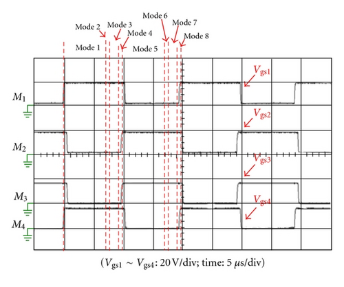
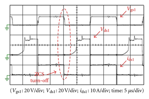
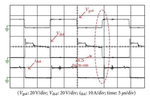
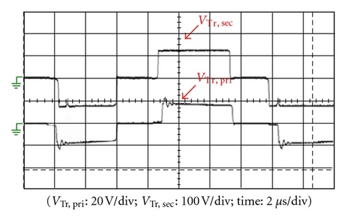
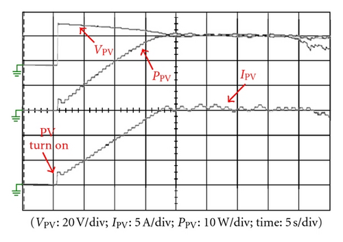
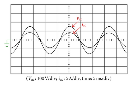
Figure 11 shows measured gate signal waveforms of power switches (M1 ~ M4). Figures 12 and 13 show measured drain-source voltage and current waveforms of the power switches M1 and M4 to illustrate a ZCS feature at turn-on or turn-off transition, respectively. In Figures 12 and 13, ringing condition appeared in voltage and current waveforms of power switches are caused by the parasitic elements of the switching devices and the transformer. Figure 14 shows measured primary and secondary voltage waveforms of transformer. Figure 15 shows measured output current, voltage, and their corresponding power from start-up to the steady state for PV with MPPT algorithm. It can be observed that the MPPT feature for the PV can be always achieved even though the output power of the PV is altered. Figure 16 shows measured inverter voltage and current waveforms under full load 300 W condition, from which it can be seen obviously that the inverter output voltage and current are sinusoidal. By using the power analyzer Voltech PM100, a power factor of 0.99 and a THD of inverter output current less than 3% are measured. For practical applications, many circuit protection functions are included in the hardware realization. Some of the testing waveforms are shown in Figure 17. Figure 17 shows measured waveforms of over-voltage, under-voltage, and over-current protection for the proposed power-generation system. From Figure 17, it can be seen that the power-generation system will be shut-down protection at once when the value of the Vdc or Idc is beyond the preset range.
6. Conclusions
In this paper, a PV power-generation system for high step-up voltage applications is proposed. All power switches of the full-bridge converter with phase-shift PWM technique have a ZCS feature at turn-on or turn-off transition. Hence, the switching losses of the power switches can be reduced. In order to draw maximum power from the PV arrays source, a simple perturbation and observation method is incorporated to realize maximum power conversion. Then, the dc-link bus is used by a dc/ac inverter, which can induce a sinusoidal source to supply utility power. To adopt a cost effective of the proposed power supply system, the MPPT algorithms and protected circuits consist of a digital signal processor (DSP) and analog circuits to implement MPPT and protect system. Thus, the control circuit of the proposed PV power-generation system is compact and programmable. Experimental results have been verified that the proposed PV power-generation system is relatively suitable for high step-up voltage applications.


