N Point DCT VLSI Architecture for Emerging HEVC Standard
Abstract
This work presents a flexible VLSI architecture to compute the N-point DCT. Since HEVC supports different block sizes for the computation of the DCT, that is, 4 × 4 up to 32 × 32, the design of a flexible architecture to support them helps reducing the area overhead of hardware implementations. The hardware proposed in this work is partially folded to save area and to get speed for large video sequences sizes. The proposed architecture relies on the decomposition of the DCT matrices into sparse submatrices in order to reduce the multiplications. Finally, multiplications are completely eliminated using the lifting scheme. The proposed architecture sustains real-time processing of 1080P HD video codec running at 150 MHz.
1. Introduction
As the technology is evolving day by day, the size of hardware is shrinking with an increase of the storage capacity. High-end video applications have become very demanding in our daily life activities, for example, watching movies, video conferencing, creating and saving videos using high definition video cameras, and so forth. A single device can support all the multimedia applications which seemed to be dreaming before, for example, new high-end mobile phones and smart phones. As a consequence, new highly efficient video coders are of paramount importance. However, high efficiency comes at the expense of computational complexity. As pointed out in [1, 2], several blocks of video codecs, including the transform stage [3], motion estimation and entropy coding [4], are responsible for this high complexity. As an example the discrete-cosine-transform (DCT), that is used in several standards for image and video compression, is a computation intensive operation. In particular, it requires a large number of additions and multiplications for direct implementation.
HEVC, the brand new and yet-to-release video coding standard, addresses high efficient video coding. One of the tools employed to improve coding efficiency is the DCT with different transform sizes. As an example, the 16-point DCT of HEVC is shown in [5]. In video compression, the DCT is widely used because it compacts the image energy at the low frequencies, making easy to discard the high frequency components. To meet the requirement of real-time processing, hardware implementations of 2-D DCT/inverse DCT (IDCT) are adopted, for example, [6]. The 2-D DCT/IDCT can be implemented with the 1-D DCT/IDCT and a transpose memory in a row-column decomposition manner. In the direct implementation of DCT, float-point multiplications have to be tackled, which cause precision problems in hardware. Hence, we propose a Walsh-Hadamard transform-based DCT implementation [7]. Then, inspired by the DCT factorizations proposed in [8, 9], we factorize the remaining rotations into simpler steps through the lifting scheme [10]. The resulting lifting scheme-based architecture, inspired by [11–13], is simplified, exploiting the techniques proposed in [9, 14] to achieve a multiplierless implementation. Other techniques can be employed to achieve multiplierless solutions, such as the ones proposed in [8, 15–18], but they are not discussed in this work. In this work, the proposed multisize DCT architecture supports all the block sizes of HEVC and is proposed for the real-time processing of 1080P HD video sequences.
The rest of this paper is organized as follows. Section 2 provides reviews of 2-D DCT transform. Section 3 shows the matrix decompositions for different DCT sizes. Section 4 presents the proposed hardware architecture. The VLSI implementation and the simulation results in Section 5. Finally, Section 6 concludes this paper.
2. Review of 2D Transform
- (1)
bit reverse the order of the rows of HN,
- (2)
gray coding to the row indices.
3. Matrix Decompositions for Different N
Matrices for different DCT are derived using the factorization presented in Section 2. In the following paragraphs factorizations for N ranging from 4 to 32 are explicitly shown.
3.1. 4 × 4 DCT
3.2. 8 × 8 DCT
3.3. 16 × 16 DCT
3.4. 32 × 32 DCT
4. Proposed Architecture
The complete hardware architecture of the DCT is shown in Figure 1. Each frame is loaded in the input frame memory. The complete frame is divided into N × N blocks. The control unit reads the rows of each block from the input memory. At the same time, the control unit passes a “1” to the input multiplexers. Also the address and other control signals are passed to the DCT block. After complete calculation of the DCT, the transformed row is input to the transpose memory, along with its corresponding address. In this way, for the first N clock cycles, the rows from the input memory are input to the DCT and are written on the corresponding addresses in the transpose memory. After the N clock cycles, the control unit passes a “0” for the input multiplexers for the next N clock cycles. So in this way, each column from the transpose memory is input to DCT block, and the outputs of the DCT block are written back in the transpose memory, on the same location from where they are read. When all the columns are read and processed by the DCT, the control unit again starts reading the next N × N block from the input memory and at the same time, each row from the transpose memory is written to the output transformed memory. In this way all the N × N blocks are read, processed, and written in the output transformed memory.
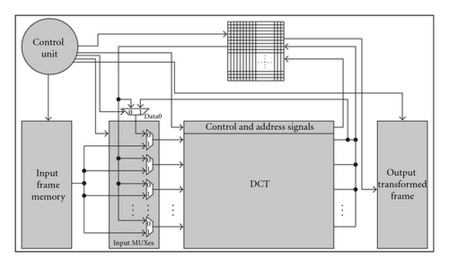
When the last row is processed through the DCT, it is written to the transpose memory. At the same time, the first column from the transpose memory is read in order to be processed through DCT block. As the last row was not written, so the last data of the first column is not valid. So “Data0” multiplexer is used for forwarding. In this way, the first output of last transformed row of a N × N block is forwarded to the input to DCT and also written to the transpose memory.
4.1. DCT Block
DCT block is the main block of the complete architecture. The DCT block takes the input data, the corresponding control signals, and the corresponding addresses. The internal architecture of the DCT block is shown in Figure 2.
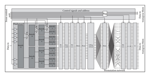
DCT block has 4 pipeline stages. The data is passed through the Hadamard block. The Hadamard block is designed with a fully parallel architecture. The Hadamard block takes 32 data at its inputs and passes to the butterfly_32, while the first 16 are input to the butterfly_16, the first 8 are input to the butterfly_8, and the first 4 are input to the butterfly_4 as well. Multiplexers are placed at the inputs of each different size butterfly in order to have correct result from Hadamard block. The select signals for the multiplexers are controlled by the control unit. The Hadamard block has 32 outputs. To have a Walsh transform from a Hadamard one, the bit_reversal and gray_code blocks are placed after the Hadamard block.
In the bit_reversal block, the data at input port number X is moved to output port number Y, where the output port number Y is determined by representation the input port number X and reversing the bits. For example, in case of DCT_16, the Hadamard block will produce 16 valid outputs. So the 16 inputs to the bit_reversal block are shuffled according to bit_reversal rule, for example, X = 0 means X = “0000" and the bit_reversal is also Y = “0000". So the first input port will be connected to the first output port. Similarly, for X = “0001", the bit reversal will Y = “1000" which means that the second input port is connected to the eight output port. In this way all the inputs are connected to the outputs according to bit reversal rule. As the architecture supports four different sizes of DCT, it means that the bit reversal rule will be different for each DCT size. For example, for DCT_4, X = “01" will be connected to Y = “10", that is, 2nd output port, while in case of DCT_16, it will be connected to the 8th output port. So multiplexers are placed in order to support all the DCT sizes in the bit reversal block.
Gray code block works in the same principle as bit reversal block, but according to gray code law. In gray code block, the output port is determined by applying gray code on the input addresses. For example, for DCT_32 if X = “01101", Y = “01011". So the input port number 13 is connected with the output port number 11. Gray code calculation does not depend on the DCT size. For example for DCT_16, if X = “1101", Y = “1011", which means that input port 13 is connected to the output port number 11, which is same as that for DCT_32.
The architecture of mem.block is shown in Figure 3. The memory block connects the first 16 inputs directly to the output ports, while the last 16 outputs are multiplexed with the latched inputs and the direct inputs. The last 16 outputs are used in case of DCT_32, while the last 16 last inputs are bypassed in case of DCT_4, DCT_8, and DCT_16.
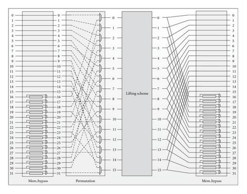
The permutation block is implemented using (27), (36), and (46). The block takes 32 inputs, and it sends 16 of the inputs to the outputs according to the permutation law. The first 16 inputs to the permutation block are passed to the outputs in the first clock cycle, while in the second clock cycle the last 16 inputs of the permutation network are passed to the outputs. In case of DCT < 32, the selection line of the multiplexers is always set to “0”, while in case of DCT = 32, the selection line remains “0” in first clock cycle, while remains “1” in the next clock cycle.
The lifting scheme is implemented using (19), (23), (31), and (40). The lifting block is implemented with a folded architecture. Where the fully parallel lifting block is used for DCT sizes of 4, 8, and 16, while DCT_32, the block is reused. Each row of DCT_32 takes 2 clock cycles for completion. During the first clock cycle, the upper 16 inputs are processed by the lifting scheme and are stored in the memory block. In the next clock cycle, the lower 16 inputs are processed by the lifting block and the result along with the previously calculated stored values is forwarded to the next block. The lifting block is shown in Figure 4.
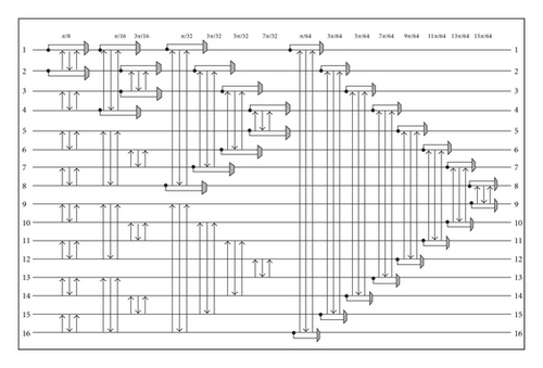
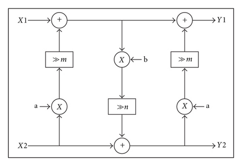
The lifting structures takes two values at the inputs. For each Givens rotation, the a, b, m, and n are approximated integer values, in order to have the approximated DCT equal to the actual DCT. As a and b are integers, the multiplications are implemented using adders and shift operations. The result of each lifting structure is quantized to 16-bits resolution to have a reasonable PSNR value. So the final outputs of the lifting block are 16-bit wide. The results of some lifting structures are bypassed using the multiplexers at their outputs. In fact, the select line for the multiplexers will always remain “0” for DCT_4, DCT_8, and DCT_16, while for DCT_32, the select line remains “0” for first clock cycle and “1” the for the next clock cycle.
In case of DCT_32, the Hadamard block produces 32 results in parallel. The outputs of the Hadamard block are fed into the bit reversal block, gray code block, and in the following bit reversal block, and the output
of the bit reversal block is fed into the memory block. The memory block passes the upper 16 inputs directly to the permutation block, while the lower 16 inputs are stored in the registers. The permutation block forwards the upper 16 inputs to the lifting scheme, where the select lines for the multiplexers in the lifting scheme are set to “0”, and the lifting scheme outputs the results and the results are stored in the following memory block. In the next clock cycle the lower 16 values stored in the first memory block are passed to the lifting scheme, through the permutation block. The selection line for the multiplexers in the lifting scheme are set to “1”. The 16 results are calculated and are passed to the memory block. At the same time, the memory block forwards the previously stored values along with the new arrived ones.
In case of DCT_4, DCT_8, and DCT_16, the lower 16 values from the first memory blocks are invalid and never used. So the valid upper 16 inputs are fed into the lifting scheme via permutation network. The selection line for the lifting scheme multiplexers is always set to “0” in case of DCT < 32.
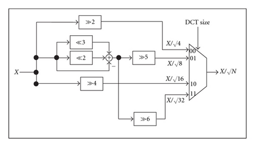
The hardware architecture of the one square root block is shown in Figure 6. The input is divided by and the calculated values are fed into the output multiplexer, where the valid result is sent to output depending on the DCT size. Finally, the outputs from the square root block are quantized from 16 bits to 13 bits using the Q block.
4.2. Transpose Buffer
Transpose buffer is designed using registers. The buffer is designed to support maximum DCT size, that is, DCT_32. So the buffer is of size N × N × B, where N = 32 and B = 13, where B is the width of each data. So a total of 13 kbits memory is utilized to implement transpose buffer. The inputs of the buffer are the clock, reset, transpose signal, the row number, the column number, read enable signal, and the write enable signal. During the direct cycle, all the rows from the input frame memory are transformed through DCT block, and the results are stored on the corresponding rows in the transpose buffer. When all the rows of a input frame memory are transformed and written to the transform buffer, the columns of the transform buffer are read and the columns are transformed via DCT block, and the results are again written back to the transform buffer in transpose way, that is, on each column. When all the columns of the transform buffer are read, transformed, and written back to the buffer, the rows of the input frame memory are read row wise, and at the same time the rows of the transform buffer are written to the output frame memory. In this way, the complete frame is transformed and written to the output memory.
4.3. Input MUXes Block
The DCT transforms the rows of the block and the results are stored in the buffer. So the select signal for the input MUXes block is set to “1”. After N clock cycles, where N is the size of DCT, the select signal of the input MUXes is set to “0”, so that the columns from the transform buffer is fed into the DCT block. So, input MUXes block switches the inputs for the DCT block for the direct or transformed cycles.
4.4. Data0 Multiplexer
During the direct cycles, the rows from the input memory are transformed and the results are written in the transform buffer. When the last row from the input memory is transformed, first column is read in the next clock cycle from the transform memory. At this point, the last data of the first column is not the valid one, as the last transformed row has not yet been written to the memory. So data0 multiplexer is used for forwarding, where the first data out of the 32 transformed dates is selected from the data0 memory. The select line of the data0 multiplexer is set to “1” for just one clock cycle during transformation of N × N block, that is, when the first column is read from transform buffer and the last row is transformed via DCT block, otherwise the select signal is always set to “0”.
4.5. Control Unit
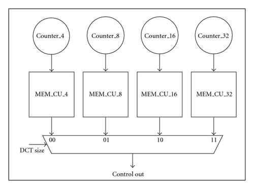
Control Unit controls the activities of all the blocks in each clock cycle. This unit is responsible for a correct sequence of operations. Control unit is designed using 4 memories, where each memory contains the control signals for each DCT size. There are 4 counters in the unit, where each counter produces the addresses for its corresponding memories. In response to the addresses, the memories output the control signals. The outputs of the memories are multiplexed, where the selection line of the multiplexer decides which input to go out. The hardware architecture of the control unit is shown in Figure 7. MEM_CU_4 is a 8 × 128 = 1 kbits size, MEM_CU_8 is a 16 × 128 = 2 kbits size, and MEM_CU_16 is a 32 × 128 = 16 kbits bits size while MEM_CU_32 is a 128 × 128 = 16 kbits size. The memories contains N control signals for direct cycle and N clock cycles for the transpose cycle, where N is the DCT size. But MEM_CU_32 contains 2(N + N) control signals, because each row or column takes two clock cycles for completion in case of DCT_32. So the control unit generates 128-bits wide control signals, for all the functioning blocks of the complete DCT in each clock cycle.
5. Results
- (1)
(N/2) · log 2(N) 2-inputs/2-output butterfly for the N-point WHT.
- (2)
1 + (N/2) · [log 2(N) − 2] 2-input/2-output lifting-based (3-lifting-step) structures for the Givens rotations.
| a | Adders | b | Adders |
|---|---|---|---|
| 51 | 2 | −98 | 2 |
| 101 | 3 | −569 | 2 |
| 311 | 3 | −200 | 3 |
| 25 | 2 | −50 | 2 |
| 152 | 2 | −297 | 3 |
| 64 | 0 | −121 | 2 |
| 183 | 3 | −325 | 3 |
| 25 | 2 | −50 | 2 |
| 19 | 2 | −38 | 2 |
| 63 | 1 | −124 | 1 |
| 178 | 3 | −345 | 4 |
| 115 | 3 | −219 | 3 |
| 71 | 2 | −132 | 1 |
| 169 | 3 | −305 | 3 |
| 99 | 3 | −172 | 3 |
According to [14], multiplications for a1, 3 = 51 and b1, 3 = −98 can be implemented with a minimum number of additions resorting to the n-dimensional reduced adder graph (RAG-n) technique. The total number of adders required for all the coefficients is shown in Table 1.
The DCT block contains 2 × N/2 × log 2(N) = 160 adders to implement the Hadamard block. Using Tables 1 and 2, the number of adders use to implement the DCT can be calculated. The first stage of lifting steps (π/8 rotation) requires 3 × 8 = 24 adders to implement the lifting structure, and further 6 × 8 = 48 adders are required to implement all the steps involving a1, 3 and b1, 3. The first stage of lifting steps (π/16 rotation) requires 3 × 4 = 12 adders to implement the lifting structure, and further 8 × 4 = 32 adders are required to implement all the steps involving a1, 4 and b1, 4. The first stage of lifting steps (3π/16 rotation) requires 3 × 4 = 12 adders to implement the lifting structure, and further 9 × 4 = 36 adders are required to implement all the steps involving a3, 4 and b3, 4. The first stage of lifting steps (π/32 rotation) requires 3 × 2 = 6 adders to implement the lifting structure, and further 6 × 2 = 12 adders are required to implement all the steps involving a1, 5 and b1, 5. The first stage of lifting steps (3π/32 rotation) requires 3 × 2 = 6 adders to implement the lifting structure, and further 7 × 2 = 14 adders are required to implement all the steps involving a3, 5 and b3, 5.
| Givens rotations | m, n | a | b |
|---|---|---|---|
| π/8 | 8 | 51 | −98 |
| π/16 | 10 | 101 | −569 |
| 3π/16 | 10 | 311 | −200 |
| π/32 | 9 | 25 | −50 |
| 3π/32 | 10 | 152 | −297 |
| 5π/32 | 8 | 64 | −121 |
| 7π/32 | 9 | 183 | −325 |
| π/64 | 10 | 25 | −50 |
| 3π/64 | 8 | 19 | −38 |
| 5π/64 | 9 | 63 | −124 |
| 7π/64 | 10 | 178 | −345 |
| 9π/64 | 9 | 115 | −219 |
| 11π/64 | 8 | 71 | −132 |
| 13π/64 | 9 | 169 | −305 |
| 15π/64 | 8 | 99 | −172 |
The first stage of lifting steps (5π/32 rotation) requires 3 × 2 = 6 adders to implement the lifting structure, and further 2 × 2 = 4 adders are required to implement all the steps involving a5, 5 and b5, 5. The first stage of lifting steps (7π/32 rotation) requires 3 × 2 = 6 adders to implement the lifting structure, and further 9 × 2 = 18 adders are required to implement all the steps involving a7, 5 and b7, 5. The first stage of lifting steps (π/64 rotation) requires 3 adders to implement the lifting structure, and further 6 adders are required to implement all the steps involving a1, 6 and b1, 6. The first stage of lifting steps (3π/64 rotation) requires 3 adders to implement the lifting structure, and further 6 adders are required to implement all the steps involving a3, 6 and b3, 6. The first stage of lifting steps (5π/64 rotation) requires 3 adders to implement the lifting structure, and further 3 adders are required to implement all the steps involving a5, 6 and b5, 6. The first stage of lifting steps (7π/64 rotation) requires 3 adders to implement the lifting structure, and further 10 adders are required to implement all the steps involving a7, 6 and b7, 6. The first stage of lifting steps (9π/64 rotation) requires 3 adders to implement the lifting structure, and further 9 adders are required to implement all the steps involving a9, 6 and b9, 6. The first stage of lifting steps (11π/64 rotation) requires 3 adders to implement the lifting structure, and further 5 adders are required to implement all the steps involving a11, 6 and b11, 6. The first stage of lifting steps (13π/64 rotation) requires 3 adders to implement the lifting structure, and further 9 adders are required to implement all the steps involving a13, 6 and b13, 6. The first stage of lifting steps (15π/64 rotation) requires 3 adders to implement the lifting structure, and further 9 adders are required to implement all the steps involving a15, 6 and b15, 6. The square root block contains 2 adders, and there are 32 square root blocks. Therefore, 64 adders are calculating square roots in parallel. The total number of adders required for Hadamard and lifting scheme is 160 + 72 + 44 + 48 + 18 + 20 + 10 + 24 + 9 + 9 + 6 + 13 + 12 + 15 + 12 + 12 + 64 = 548.
| Sequences | DCT size | |||||||||||
|---|---|---|---|---|---|---|---|---|---|---|---|---|
| N = 4 | N = 8 | N = 16 | N = 32 | |||||||||
| Y | U | V | Y | U | V | Y | U | V | Y | U | V | |
| BQ terrace_1920 × 1080_60 | 47.1 | 44.4 | 44.1 | 48.8 | 45.9 | 44.1 | 48.9 | 45.4 | 45.3 | 48.8 | 45.7 | 44.1 |
| BQ square_416 × 240_60 | 47.4 | 45.1 | 45.2 | 48.1 | 45.2 | 45.2 | 48.1 | 45.7 | 44.1 | 48.2 | 45.2 | 44.7 |
| BQ mall_832 × 480_60 | 46.9 | 44.1 | 44.5 | 47.9 | 44.9 | 45.5 | 48.7 | 44.6 | 44.9 | 48.4 | 45.7 | 45.3 |
| Basketball drive_1920 × 1080_50 | 47.8 | 44.5 | 44.1 | 48.2 | 44.8 | 45.7 | 48.5 | 45.1 | 45.7 | 48.3 | 45.1 | 45.3 |
| Basketball drill_832 × 480_50 | 47.0 | 45.4 | 45.6 | 48.6 | 45.0 | 44.8 | 48.2 | 45.9 | 45.0 | 48.7 | 45.4 | 45.5 |
In Tables 4, 5, and 6, the number of multiplications, additions, and shifts, required to calculate different sizes of DCT, are shown. The proposed architecture has no multiplications, where all the multiplications are implemented using shifts and adds. As it can be observed, the number of additions required to compute the 32-point DCT with the proposed architecture is less than the original DCT implementation and the other proposed ones.
| N | M | A | S |
|---|---|---|---|
| 4 | 0 | 17 | 5 |
| 8 | 0 | 74 | 39 |
| 16 | 0 | 232 | 132 |
| 32 | 0 | 548 | 249 |
- *N is the DCT size.
- *M is the number of multiplications.
- *A is the number of additions.
- *S is the number of shifts.
| M | A | S | |
|---|---|---|---|
| Original | 1024 | 992 | 0 |
| Proposed | 0 | 548 | 249 |
| M | A | S | |
|---|---|---|---|
| [5] | 0 | 242 | 58 |
| Proposed | 0 | 232 | 132 |
- *N is the DCT size.
- *M is the number of multiplications.
- *A is the number of additions.
- *S is the number of shifts.
The net list is written in VHDL language. Synopsys Design Vision is used for synthesis purpose. The code is synthesized on 90 nm standard cell library at a clock frequency of 150 MHz. Table 7 shows the results of the synthesis.
| Parameter | Value |
|---|---|
| Technology | 90 nm |
| Frequency | 150 MHz |
| Area | 0.42 mm2 |
| Power | 884.1 μW |
| Memory | 36 kbits |
6. Conclusion
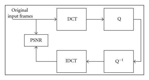
In this work, a dynamic N-point DCT for HEVC is proposed. A partially folded architecture is adopted to maintain speed and to save area. The DCT supports 4, 8, 16, and 32 points. The simulation results show that the PSNR is very close to 50 dB, which is reasonably good. Multiplications are removed from the architecture by introducing lifting scheme and approximating the coefficients.


