Fabrication and Photovoltaic Characteristics of Coaxial Silicon Nanowire Solar Cells Prepared by Wet Chemical Etching
Abstract
Nanostructured solar cells with coaxial p-n junction structures have strong potential to enhance the performances of the silicon-based solar cells. This study demonstrates a radial junction silicon nanowire (RJSNW) solar cell that was fabricated simply and at low cost using wet chemical etching. Experimental results reveal that the reflectance of the silicon nanowires (SNWs) declines as their length increases. The excellent light trapping was mainly associated with high aspect ratio of the SNW arrays. A conversion efficiency of ~7.1% and an external quantum efficiency of ~64.6% at 700 nm were demonstrated. Control of etching time and diffusion conditions holds great promise for the development of future RJSNW solar cells. Improving the electrode/RJSNW contact will promote the collection of carries in coaxial core-shell SNW array solar cells.
1. Introduction
Nanostructured solar cells with high efficiency and low cost are being considered to meet the urgent need for third-generation solar cell applications. Recent studies have shown that silicon nanowires (SNWs) that are prepared by the vapor-liquid-solid (bottom up) and wet chemical etching approaches (top down) can be employed to enhance the photovoltaic characterization because such SNW arrays have very low reflectance [1–12]. Theoretical studies have indicated that coaxial SNW structures with sub-5 nm p-n junction structures have potentiality to realize ultrahigh efficiencies due to the tunable energy bandgap [13]. Moreover, the cause of the conversion efficiency improvement can be attributed to the short collection length in radial p-n junction SNW [14]. The properties of SNWs are determined by the enhanced surface area to volume ratio. Theoretical calculations have also predicted that a direct energy bandgap exists in the 4.5–5.3 nm range for SNWs that are oriented in the 〈111〉 direction [15]. The bandgap increases as the diameters of the SNWs decrease in the 7–1.3 nm range [16]. Accordingly, SNW solar cells are promising for their scalability as nanostructured solar cells. However, the conversion efficiencies (CEs) of SNW solar cells are not yet large enough. SNW solar cells on metal foil with a current density of 1.6 mA/cm2, an external quantum efficiency (EQE) of 12% at 690 nm, and a conversion efficiency of 0.1% have been described [5]. Individual core-shell SNW photovoltaic elements with an open-circuit voltage (Voc) of 260 mV, a short-circuit current (Isc) of 0.503 nA, and a fill factor (FF) of 55.0% have been demonstrated [6]. Radial junction SNW (RJSNW) solar cells with a Voc of 290 mV, a short-circuit current density (Jsc) of 4.28 mA/cm2, and an FF of 33.0% have also been demonstrated [7]. Electrolessly etched SNW solar cells with a Jsc of 1.36 mA/cm2 and a Voc of 730 ± 20 mV have been proposed [17]. Moreover, a lot of SNWs fabricated by metal-assisted chemical etching have demonstrated their application potentials [18–21]. Thus, this study will scrutinize the etching time and the diffusion conditions of RJSNWs.
2. Experimental Methods
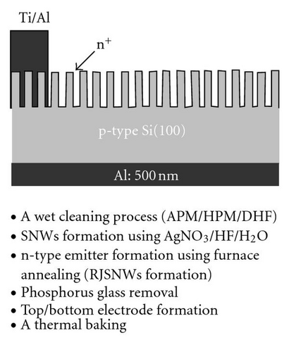
Square samples with an area of 4 cm2 were cut from (100)-oriented p-type silicon [p-Si(100)] wafer with ρ = 0.5–3 Ωcm. The thicknesses of all p-Si (100) wafers were approximately 210 ± 30 μm. All samples were firstly cleaned by a wet cleaning process (APM/HPM/DHF), using an NH4OH/H2O2/H2O mixture (APM) in a ratio of 1 : 4 : 20 (volume) at 75°C and an HCl/H2O2/H2O mixture (HPM) in a ratio of 1 : 1 : 6 (volume) at 75°C, to remove residues and contaminants. The dipping time in all processes was 10 min. Diluted HF (DHF) with an HF : H2O ratio of 1 : 100 (volume) was used to remove native oxide. Following the wet processes, all of the samples were rinsed in deionized water for 10 min. Then, the square p-Si(100) wafers were immersed in an aqueous AgNO3/HF/H2O mixture chemical solutions [22]. The detailed process conditions of aqueous AgNO3/HF/H2O mixture chemical solutions are summarized in Table 1. The concentration of AgNO3 was set to 1 mol L−1. Subsequently, all SNW/p-Si(100) structures were etched in nitric acid solution to eliminate the residual Ag dendrites that were observed on the surface and in between the SNWs. Phosphorosilicafilm (5 × 1020 cm−3) is a dopant formulation designed to produce phosphorous diffused layers in SNW/p-Si(100) structures by spin on coating. Then, the SNW/p-Si(100) structures coated with phosphorosilicafilm were performed by thermal phosphorus diffusion in a quartz tube furnace at 950°C in nitrogen ambient for 2.5, 3, 4, and 5 hrs as shown in Table 2. After the phosphorus glass was removed by DHF solution and rinsed in deionized water, the front electrodes of the RJSNWs were deposited by the vacuum sputtering of Ti (~30 nm) followed by Al (~500 nm) through a metal shadow mask. The rear Al (~500 nm) contacts were formed by sputtering. Finally, thermal baking was carried out in N2/H2 ambient at 450°C for 15 min to improve the quality of the Ohmic contacts. Figure 1 schematically depicts the device structure of an RJSNW solar cell with an area of 4 cm2. All samples were observed using a secondary electron microscope (SEM), an ultraviolet/visible/near infrared spectrometer, and a current-voltage (I-V) measuring device. The I-V characteristics of all solar cells were measured under AM1.5 class 3A illumination source with at 25°C. Full spectrum solar simulator lamp type is 300 W Xenon. A profile of phosphorus concentration in the n-type emitter layer was obtained by secondary ion mass spectroscopy (SIMS).
| Sample split | AgNO3/HF/H2O (volume) | Etching time (min) |
|---|---|---|
| S1 | 2 : 34: 164 | 10 |
| S2 | 4 : 34 : 162 | 10 |
| S3 | 6 : 34 : 160 | 10 |
| S4 | 8 : 34 : 158 | 10 |
| S5 | 4 : 31 : 165 | 10 |
| S6 | 4 : 38 : 158 | 10 |
| S7 | 4 : 41.5 : 154.5 | 10 |
| S8 | 4 : 34 : 162 | 1.5 |
| S9 | 4 : 34 : 162 | 3 |
| S10 | 4 : 34 : 162 | 30 |
| Sample split | AgNO3/HF/H2O 4 : 34 : 162 (volume) Etching time (min) | Diffusion time (min) |
|---|---|---|
| S11 | 1.5 | 2.5 |
| S12 | 1.5 | 3 |
| S13 | 3 | 3 |
| S14 | 30 | 3 |
| S15 | 1.5 | 4 |
| S16 | 1.5 | 5 |
3. Results and Discussion
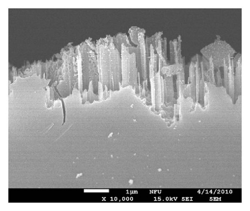
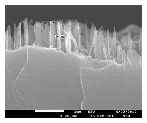
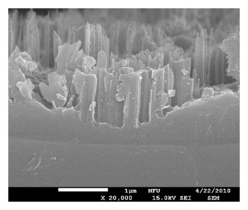
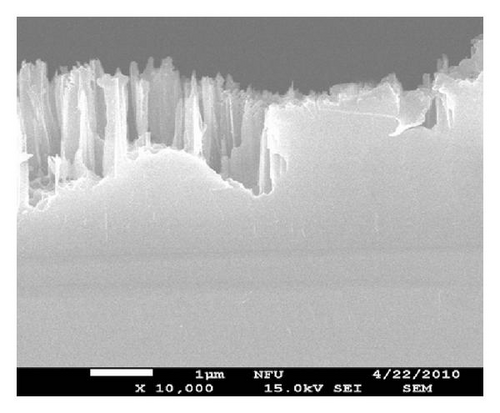
Various AgNO3 and HF concentrations in AgNO3/HF/H2O mixture chemical solutions, as well as etching time, were employed to explore various surface morphologies of SNWs formed on the p-type Si(100) substrate. To observe all of the morphologies of the SNW array structures, plane and oblique SEM images of SNW/p-Si(100) structures were obtained and presented in Figures 2–4. Figure 2 shows various SEM images of various SNW/p-Si(100) structures. Etching conditions were aqueous AgNO3/HF/H2O mixture chemical solution in a ratio of (a) 2 : 34 : 164, (b) 4 : 34 : 162, (c) 6 : 34 : 160, and (d) 8 : 34 : 158 (volume), respectively, at 25°C for 10 min. The concentration of AgNO3 in AgNO3/HF/H2O mixture chemical solution was increased. It can be seen that short SNWs were formed on the p-type Si(100) substrate resulting from low AgNO3 concentration as shown in Figure 2(a). On the contrary, the long SNWs were demonstrated using high AgNO3 concentration in AgNO3/HF/H2O mixture chemical solution as shown in Figure 2(d). Thus, the results suggest that the length of SNW increases with increasing concentration of AgNO3 in AgNO3/HF/H2O mixture chemical solution.
To realize the effects of HF concentrations in AgNO3/HF/H2O mixture chemical solutions, etching conditions were aqueous AgNO3/HF/H2O mixture chemical solution in a ratio of (a) 4 : 31 : 165, (b) 4 : 38 : 158, and (c) 4 : 41.5 : 154.5 (volume), respectively, at 25°C for 10 min, and presented in Figure 3. Compared with high HF concentration, the short SNWs were formed by AgNO3/HF/H2O mixture chemical solution with low HF concentration. Therefore, the results indicate that the length of SNWs decreases with decreasing HF wt% in AgNO3/HF/H2O mixture chemical solutions. It has been reported that the Si atoms are oxidized and dissolved at the interface between the Ag metal and the Si substrate and that the reagent and byproduct diffuse along this interface [23]. Thus, the densities and lengths of SNWs increase with increasing HF and AgNO3 concentration in aqueous AgNO3/HF/H2O mixture chemical solution.
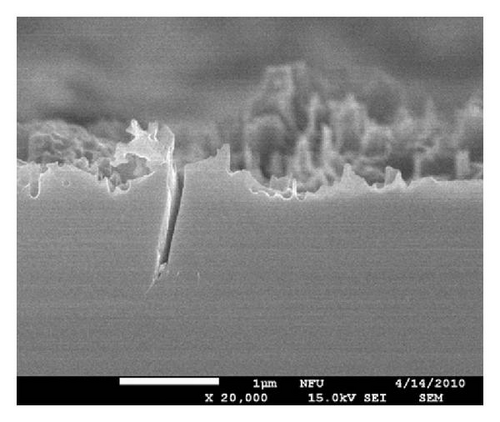
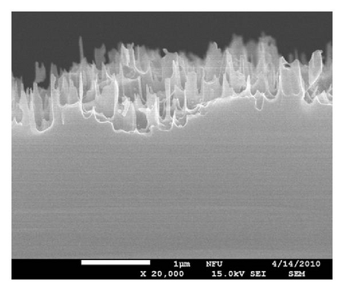
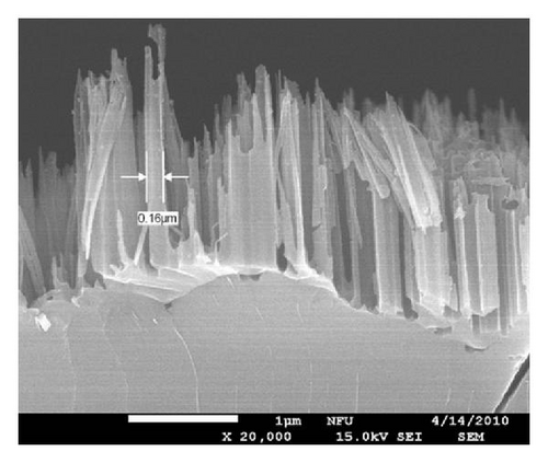
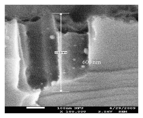
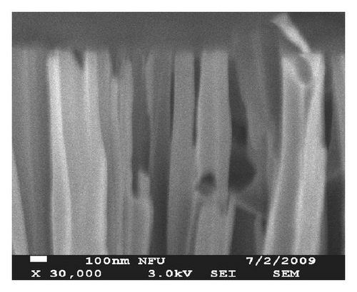
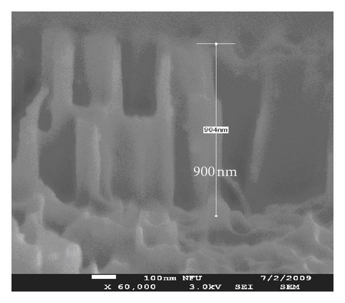
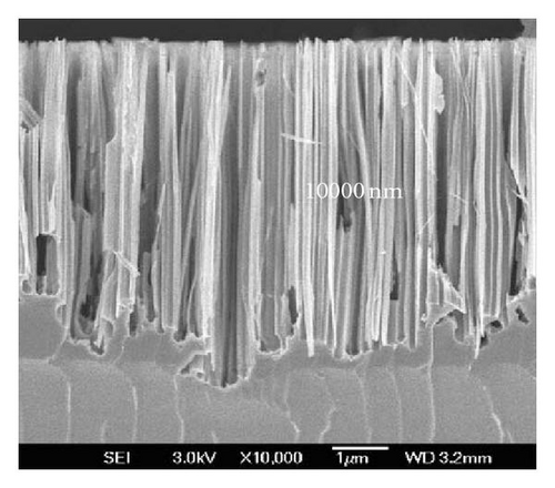
Figure 4 shows various SEM images of various SNW/p-Si(100) structures. Etching conditions were aqueous AgNO3/HF/H2O mixture chemical solution in a ratio of 4 : 34 : 162 (volume) at 25°C for (a) 1.5, (b) 3, and (c) 30 min, respectively. The lengths of the SNW arrays ranged from 600 to 10000 nm and depended critically on the etching time. These results suggest that the densities and the lengths increased with the duration of wet chemical etching. Thus, the SNWs can be obtained by a suitable tuning AgNO3 and HF concentrations in AgNO3/HF/H2O mixture chemical solutions.
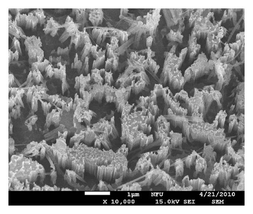
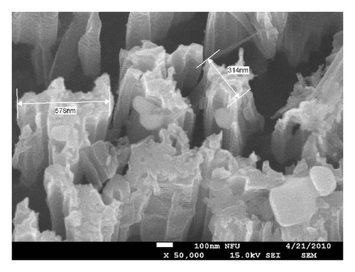
Figure 5 shows the top morphologies of the SNW/p-Si(100) structure at magnifications of (a) ×10k, and (b) ×50k. The etching condition was an aqueous AgNO3/HF/H2O mixture chemical solution with a ratio of 4 : 34 : 162 (volume) at 25°C for 3 min. The cross-sections of SNW arrays exhibited nonregular morphologies and their sizes ranged from 300 to 1000 nm. The SEM images in Figure 5 also indicate that the surface of SNWs exhibited nanostructured texturization. Research has demonstrated that the nanostructure textured arrays at silicon surfaces prepared by a wet chemical process have low reflection [24]. In this study, SNW arrays with a larger aspect ratio of around 40 : 1 were obtained after an etching time of 30 min. Accordingly, the SNW arrays with various aspect ratios and microstructural arrays will play a main role of the light trapping.
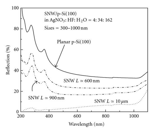
To elucidate the reflectance characteristics of various SNW arrays, reflectance spectra of various SNW/p-Si(100) structures were obtained and shown in Figure 6. An integrating sphere was used to ensure that all reflected light was captured over all angles. The diameter of the integrating sphere was 60 mm. The reflectance spectra confirm that the reflectance of SNW arrays decreases as their lengths increase. The excellent trapping of light was mostly associated with the high aspect ratio of the SNW arrays. Figure 6 also shows the reflectance spectrum of planar p-Si(100) substrate as a reference. The planar p-Si(100) structure had a larger reflectance than SNWs. Hence, SNW arrays with a high aspect ratio can have a very low reflectance, and SNW arrays with low reflectance have potential for use as antireflective coatings (ARCs) of solar cells.
The n-type emitter layer in p-n junction silicon solar cell is usually doped to a level that suffices to conduct away the generated carriers without causing resistive loss. However, excessive levels of doping reduces carrier lifetime to the extent that carriers recombine before reaching the p-n junction. Therefore, the n-type emitter layers of SNW arrays with various diffusion times as shown in Table 2 were utilized to optimize the characteristics of the emitter layer. The n-type SNW/p-Si(100) structures in this investigation were formed by the diffusion of phosphorus at 950°C in nitrogen ambient for 3 hrs, resulting in an emitter with a depth of approximately 150 nm, as presented in Figure 7. The resistivity of the p-type substrate was 0.5–3 Ωcm, corresponding to a doping density of approximately 5 × 10¹⁵~6 × 1016 cm−3 [25]. The higher phosphorous concentrations in Figure 5 (>3 × 1016 cm−3) were detected when the junction depth lowered 150 nm. Hence, an emitter layer thickness of approximately 150 nm was extrapolated. A p-type SNW with a cross-section size of smaller than 300 nm was converted to an n-type SNW by diffusion at 950°C in nitrogen ambient for 3 hrs. However, the cross-section sizes of the SNW arrays ranged from 300 to 1000 nm. Most SNWs dimensions were larger than 300 nm, according to their morphologies presented in Figure 5. Thus, most coaxial core-shell-type p-n junction SNWs were demonstrated. The modulation of etching time and diffusion conditions is very promising for the future development of RJSNW solar cells.
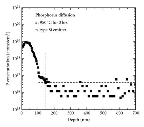
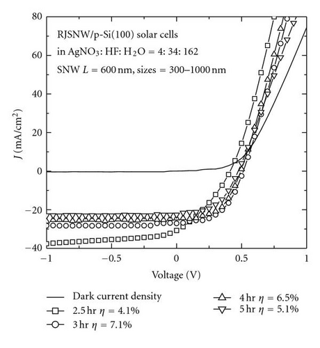
Figure 8 plots current density-voltage (J-V) curves of various n-type SNW/p-Si(100) structured solar cells, obtained in the dark and under illumination (AM 1.5). The efficiencies were measured under the global AM1.5 spectrum (1000 W/m2) at 25°C. An improved CE of approximately 7.1% with a Jsc of 27 mA/cm2, a Voc of 500 mV, and an FF of 52% was obtained for an RJSNW array solar cell sample with a diffusion time of 3 hrs. Etching conditions were aqueous AgNO3/HF/H2O mixture chemical solution in a ratio of 4 : 34 : 162 (volume) at 25°C for 1.5 min. The current density ranged from 0 to −1 V in the saturation current density region. Since heavy doping under contacts keeps minority carriers away from high recombination front contact, the saturation current density of the 2.5 hr sample is higher than that of the 3 hr sample. Thus, the open-circuit voltage of the 2.5 hr sample is smaller than that of the 3 hr sample as shown in Figure 8 due to larger saturation current density of the 2.5 hr sample. Therefore, based on the results of Figure 8, diffusion was carried out at 950°C for 3 hrs to examine the effects of SNW array length on the photovoltaic characteristics of RJSNW solar cells.
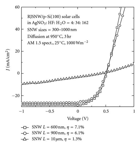
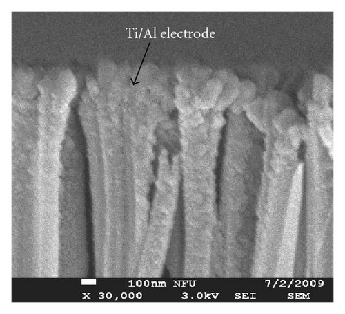
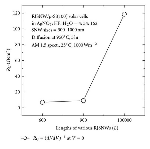
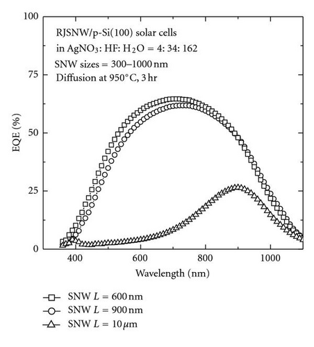
To understand the mechanism of improvement, the external quantum efficiencies (EQEs) of various RJSNW solar cells were measured for incident light with wavelengths of 350~1100 nm, as shown in Figure 12. The reduced EQE in low and long wavelengths is well known to be associated with recombination at the front and rear surfaces. At medium wavelengths, reflection and a low carrier diffusion length reduce overall QE. A shorter SNW solar cell has a larger EQE, implying that the origin of the increase is related to effective carrier conduction away from the p/n junction, associated with a short electrode/RJSNW contact. The photovoltaic property of the RJSNW solar cell with a maximum EQE value of ~64.6% at 700 nm was measured.
4. Conclusions
The photovoltaic characteristics of radial junction silicon nanowire (RJSNW) solar cells were demonstrated by the wet chemical etching of a p-type Si(100) wafer. An improved conversion efficiency of approximately 7.1% with a Jsc of 27 mA/cm2, a Voc of 500 mV, and an FF of 52% was obtained for an RJSNW array solar cell sample with a diffusion time of 3 hrs. Etching conditions were aqueous AgNO3/HF/H2O mixture chemical solution in a ratio of 4 : 34 : 162 (volume) at 25°C for 1.5 min. Experimental results reveal that this RJSNW solar cell is a promising candidate for the development of nanostructured solar cells.
Acknowledgments
The authors would like to thank the National Science Council of the Republic of China for the financial support under Contract nos. NSC 100-2221-E-150-087 and NSC 100-2622-E-150-027-CC3. Technical support from National Nano Device Laboratories (NDL) of the Taiwan and Common Laboratories for Micro/Nano Science and Technology of National Formosa University is also acknowledged.


