The Compromise Condition for High Performance of the Single Silicon Heterojunction Solar Cells
Abstract
For optimum performance of the hydrogenated amorphous silicon/crystalline silicon (a-Si : H/c-Si) heterojunction solar cells, featuring a doping concentration, localized states, as well as thickness of emitter layer are crucial, since Fermi level, surface passivated quality, and light absorption have to be compromised themselves. For this purpose, the effect of both doping concentration and thickness of emitter layer was investigated. It was found that with gas phase doping concentration and emitter layer thickness of 3% and 7 nm, solar cell efficiency in excess of 14.6% can be achieved. For high gas phase doping concentration, the degradation of open-circuit voltage as well as cell efficiency was obtained due to the higher disorder in the emitter layer. The heavily doped along with thicker in thickness of emitter layer results in light absorption on short wavelength, then diminishing short-circuit current density.
1. Introduction
Heterojunction solar cells consisting of crystalline silicon (c-Si) and hydrogenated amorphous silicon (a-Si : H) offer a low cost and high efficiency energy conversion alternative to conventional crystalline silicon solar cells. Compared to conventional silicon solar cells with diffused n/p junction and back surface field layers (BSF), noteworthy cost reduction can be obtained due to a completely low temperature (~200°C) formation process for both the n/p junction and BSF layer using hydrogenated amorphous silicon technology. Presently, Sanyo’s heterojunction with intrinsic thin layer (HIT) solar cells showed the world record efficiency of 23% for double-junction structure [1]. However, for the single-junction HIT solar cell fabricated on polished wafers has reported approximately 13 ~ 14% efficiency [2–6], in which the open-circuit voltage (Voc) did not exceed 580 mV, and the fill factor 74% could be obtained. Beside Sanyo, most research groups have been working on single-junction HIT solar cell using p-type c-Si as a base substrate.
When using a-Si : H and c-Si for junction formation, there are different aspects to be taken into account. Firstly to obtain high open circuit voltage (Voc) and thus efficiency, the Fermi level in the emitter layer should be as close as to the nearest band as possible, which means that doping concentration is as high as it could be. The high doping concentration, nevertheless, also results in the high defect density in the films and leads to enhanced surface recombination [4]. The preferred doping concentration of emitter for HIT solar cell performance is still a matter of discussion. Sanyo’s group has held world record efficiency of 23%, despite of, the limitation outside of Sanyo because of improper deposition condition such as doping concentration and so on. E. Conrad et al. suggested an optimal doping concentration (B2H6/SiH4) of around 2000–3000 ppm [7]. Using simulation, N. Hernández-Como et al. proposed that the efficiency increases with increasing emitter doping concentration. Above a concentration of 3 × 10¹⁹ (cm−3), the solar cell efficiency reaches its saturation value [8].
Also the emitter thickness variation could determine the short-circuit current as well as built-in potential in case of very thin layer of a-Si : H(p). On raising the emitter thickness, a-Si : H(p) layer incorporated into solar cells acts as a “dead layer” and no electrons generated within the emitter layer are extracted due to intense carrier recombination within the defect emitter layer [9]. Reports on the optimum conditions varied in the literature and they can be classified roughly into two groups. Most research groups argue that 4 ~ 5 nm is thick enough for good device performances [1, 9]. While, emitter thickness of around 15 nm is mentioned to be thin enough by another [10]. In this paper, the compromise conditions for doping concentration, as well as the thickness of emitter layer, were investigated to set up a baseline for single p/n heterojunction solar cells.
2. Experiment
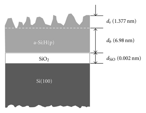
The commercial Czochralski-grown (CZ) c-Si(n) substrate with <100> orientation, resistivity of 1–10 Ω·cm, and 525 μm thickness has been used to fabricate the HIT solar cells. The crystalline Si substrates were treated by a sequence consisting of (1) acetone/methanol/DIW cleaning, (2) RCA cleaning. Native oxide was removed by a 1 min. dip in 1% hydrofluoric acid right before a-Si : H deposition. To change the doping concentration of the a-Si : H emitter, the gas phase doping concentration, B2H6/SiH4, was varied in range of 2 to 10%, while the thickness of the a-Si : H emitter was fixed at 7 ± 0.05 nm. For the emitter thickness variation set, the gas phase doping concentration was 3%, the optimization condition in previous set, while emitter thickness varied in range of 3–15 nm. For the transparent conductive oxide (TCO), Indium Tin Oxide (ITO) thin film was deposited by rf magnetron sputtering at a substrate temperature of 200°C with thickness of about 80 ± 5 nm, followed by the deposition of silver/aluminum finger as the emitter contacts. Aluminum was evaporated on backside to create a good ohmic contact prior to area defining with mesa etching.
| Xg | ds (nm) | db (nm) | dSiO (nm) | A | E0 (eV) | C | Eg (eV) |
|---|---|---|---|---|---|---|---|
| 2% | 1.978 | 7.082 | 0.052 | 80.88 | 3.97 | 1.69 | 1.62 |
| 3% | 1.377 | 6.980 | 0.002 | 83.67 | 3.91 | 1.75 | 1.62 |
| 5% | 0.909 | 7.071 | 0.154 | 93.96 | 3.84 | 1.82 | 1.59 |
| 10% | 1.880 | 6.992 | 0.032 | 95.75 | 3.83 | 1.97 | 1.60 |
3. Results and Discussion
From Figure 2, it is observed that the Ea decreases rapidly when Xg (Xg = [B2H6]/[SiH4]) is increased from 2% to 3% and then it seems to saturate with further increase. As evidence from Figure 2(a), the minimum Ea is obtained for Xg = 10% and thus the best device performance should be obtained using this gas phase doping concentration. However, contrary to our expectations, the highest performance of device is observed for Xg = 3%. The efficiency decreases for both higher and lower gas phase doping concentration. A similar variation is also observed for short-circuit current density (Jsc). The Voc increases to a value of around 590 mV with the increasing in Xg of 3% and then seems to linearly shrink for further increase of Xg increases.


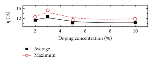
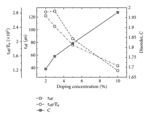
Figure 3 summarizes the degree of disorder (C) in a-Si:H(p) and minority carrier lifetime (τeff) of a-Si:H(p) deposited on c-Si(n) as a function of gas phase doping concentration of emitter layer. It is note that the C value is obtained from a well fit of the dielectric function of a-Si:H(p) using Tauc-Lorentz model, as discussing in the experimental part. It is clear that the trend of τeff and C displays a contrary direction and hence this also could be the reason for the reducing of Voc when Xg is increased. As reported by R. A. Street, substitutional doping of a-Si : H(p) leads to the creation of deep defects [13]. This leads to a self-compensation effect in a-Si:H(p). Hence, the disorder in the a-Si : H(p) leads to a higher amount of interface states and thus a decreased minority carrier lifetime of a-Si : H(p)/c-Si(n) heterojunction. By increasing gas phase doping concentration, eventually, on the one hand the band bending increases with increasing gas phase doping concentration, on the other hand the disorder in the a-Si : H layer and interface states (decrease in τeff) increases. Therefore, we suggest a new factor (Opt = τeff/ Ea) that may be presented as a trade-off between interface states and the position of the Fermi energy as showed in Figure 3. The highest Opt value is achieved at gas doping concentration of 3% and it is also point of merit for achieving highest device performance.
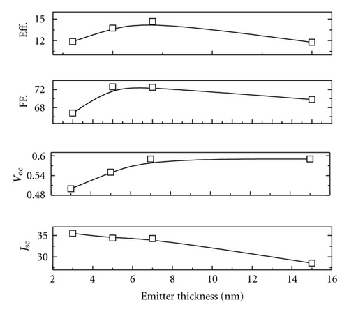
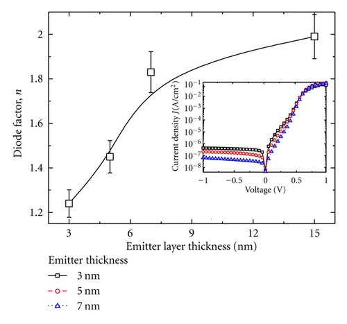
In contract to Voc, Jsc reduces with increasing emitter-layer thickness. As a result, we obtained a solar cell efficiency of 14.6% (Voc = 590 mV, FF = 0.72, and Jsc =34.3 mA/cm2) at the optimum thickness of p = 7 nm without the incorporation of surface texture, intrinsic hydrogenated amorphous silicon. In Figure 6, the external quantum efficiency (QE) spectrum as a function a-Si : H(p) thickness was depicted. For convincing, transmittance of a-Si : H(p) layer with difference thickness was also measured and shown in the inset of Figure 6. It is clear that the thicker in emitter layer leads to lower in transmittance due to Lambert-Beer law. Thus, the QE of the thinner film is enhanced especially in the short wavelength region where the absorption of the a-Si : H films is low. Hence, the reduction in Jsc shown in Figure 4 may come from the degradation of the short wavelength response. It is well known that heavily doped a-Si : H layers generally exhibit quite high defect densities of ~1018 cm−3, which is close to the defect densities of our a-Si:H(p) layer (2.33 ~ 3.70 × 1018 cm−3), separately estimated by ellipsometry measurement on a-Si : H(p) films deposited on glass substrate. Due to its structure disorder and high doping, on the one hand, the diffusion length of the carrier in amorphous silicon layer is so small that only drifts current but no diffusion current can occur. On the order hand, the penetration depth of the space charge region in the a-Si : H side is so small that there is no electric field inside the layer. Thus, a heavily doped a-Si : H(p) layer incorporated into the heterojunction solar cells acts as a “dead layer”. For that reason it has to be as thin as possible.

4. Conclusion
In conclusion, the a-Si : H(p)/c-Si(n) heterojunction solar cell was set up for future development of high efficiency heterojunction with intrinsic thin (HIT) layer solar cells. The correlation between doping concentration, a-Si : H(p) layer thickness, and cell performance was discussed. An optimum value for gas phase doping concentrations of a-Si : H(p) was found to be 3%. For high gas phase doping concentrations, on the one hand the band bending increases with increasing gas phase doping concentration, on the other hand the disorder in the a-Si : H layer and interface states (decreases in τeff) increases. Hence, solar cell efficiency degrades. The a-Si : H(p) thickness of 7 nm is optimum for a-Si : H(p)/c-Si(n) heterojunction solar cell. Degradation of open-circuit voltage or short-circuit current density and hence efficiency was observed for thinner or thicker layers. Using optimized conditions, we obtained 14.67% efficiency for the a-Si : H(p)/c-Si(n) structure.
Acknowledgment
This research was supported by WCU (World Class University) program through the National Research Foundation of Korea funded by the Ministry of Education, Science and Technology (R31-2008-000-10029-0).


