Annealing-Induced Modifications in Physicochemical and Optoelectronic Properties of Ag-Doped Nanostructured CdS Thin Films
Abstract
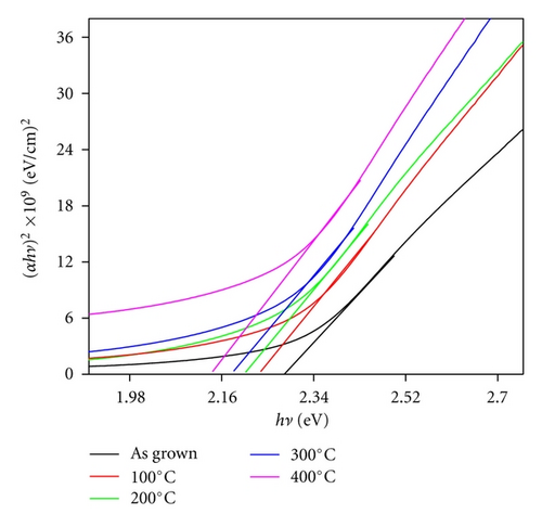
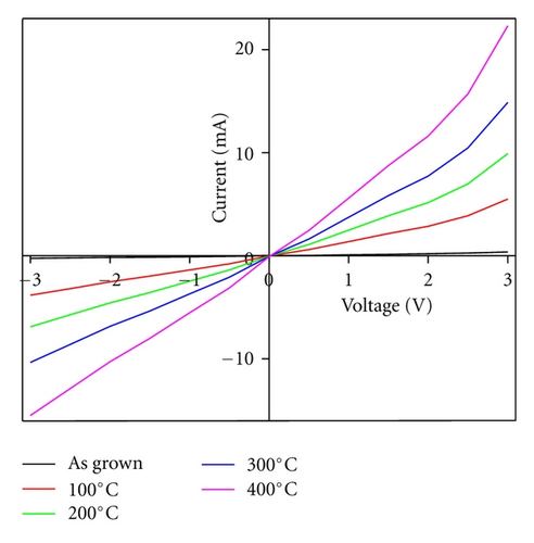
The Ag-doped nanostructured CdS thin films are grown by simple, cost effective chemical ion exchange technique at room temperature on ITO-coated glass substrate. These as grown thin films are annealed at 100, 200, 300, and 400°C in air atmosphere for 1 hour. To study the effect of annealing on physicochemical and optoelectronic properties, these as grown and annealed thin films are characterized for structural, compositional, morphological, optical, and electrical properties. X-ray diffraction (XRD) pattern reveals polycrystalline nature of these thin films with increase in crystallite size from 6.4 to 11.2 nm, from XRD the direct identification of Ag doping in CdS thin films cannot be judged, while shift in characteristics peak position of CdS is observed. The Raman spectrum represents increase in full width at half maxima and intensity of characteristic peak, confirming the material modification upon annealing treatment. Presence of Cd, Ag, and S in energy dispersive X-ray analysis spectra (EDAX) confirms expected elemental composition in thin films. Scanning electron microscopy (SEM) images represent grain growth and agglomeration upon annealing. Red shift in optical absorbance strength and energy band gap values from 2.28 to 2.14 eV is obtained. I-V response obtained from as grown and annealed thin films shows an enhancement in photosensitivity from 72% to 96% upon illumination to 100 mW/cm2 light source.
1. Introduction
Nanostructured CdS thin films are the promising compounds for various industrial and household applications because of its potential physicochemical and optoelectronic properties such as wide energy band gap (Eg = 2.42 eV), n-type conductivity, and high absorbance coefficient [1, 2]. CdS thin films are generally used as a window layer material associated with p-type conductivity, absorber layer for heterojunction solar cell applications [3, 4]. However, the high resistivity of CdS thin film limits the output values of such heterostructure, therefore to reduce the resistivity and produce the desired property CdS thin films, an Ag doping is carried out [5, 6]. The specific stoichiometry, surface morphology, crystalline quality, and nanostructured properties of Ag-doped CdS thin films make it potential material for solar cell and sensor applications. Therefore, the investigation of Ag-doped nanostructured CdS thin films is of critical importance for development of applicable device, therefore considering the multiple applications of these thin films number of research groups have prepared it by various methods. But considering the requirement of sensor, that is, stoichiometry, surface morphology, crystallinity and production cost, and so forth, the chemical bath deposition method is more useful. This technique is most inexpensive, suitable for synthesis of uniform and large area deposition. The films grown by this technique are generally polycrystalline, pin hole free, and stoichiometric [7]. Hence in utilization of Ag-doped nanostructured CdS thin films for optoelectronic applications the crystalline quality, surface morphology provides the scope for future research, therefore to improve these physicochemical and optoelectronic properties, postdeposition treatment such as annealing in air or swift heavy ion irradiation can be performed, but considering the cost as an issue, annealing in air is an affordable and useful technique for providing economically viable devices [8–10].
Therefore considering the wide application of Ag-doped CdS thin films, in the present work we have deposited Ag-doped CdS thin films by cost-effective chemical route at room temperature and the effect of annealing at 100, 200, 300, 400°C on physicochemical and optoelectronic properties has been studied and discussed.
2. Experimental Details
In next stage these as deposited CdS thin films are used for Ag doping by chemical bath deposition at room temperature using 1% AgNO3 solution prepared in distilled water. For Ag doping the CdS thin films are dipped in AgNO3 solution for 10 second [11]. These as grown Ag-doped CdS thin films are annealed at 100, 200, 300, and 400°C in air atmosphere.
These as grown and annealed, Ag-doped nanostructured CdS thin films are characterized for structural, compositional, morphological, optical, and electrical properties. The structural properties are studied using X-ray diffraction pattern (XRD) obtained on Bruker AXS, German (D8 Advanced) diffractometer in scanning range 20–60° (2θ) using CuKα radiation having 1.5406 Å wavelength. The Raman spectrum is measured using Raman spectrometer Renishaw model In-via Raman microscope using Argon ion LASER excitation of 514 nm (5 mW power) over the range 300 to 2100 cm−1. The elemental composition and surface morphology are studied with the help of energy dispersive X-rays analysis (EDAX) spectra and scanning electronic microscopy (SEM) obtained from JEOL-JSM-6360. The optical characterization performed using UV-Vis spectrophotometer Perkin Elmer, Lambda-25 in absorbance mode as a function of wavelength in 400 to 1100 nm range. The photovoltaic response measured using current voltage (I-V) characteristics under dark and illumination to 100 mW/cm2 light source using Lab equip. model 2004 interfaced with computer.
3. Results and Discussion
3.1. X-Ray Diffraction (XRD) Pattern
The XRD pattern of as grown and annealed Ag-doped CdS thin films are represented in Figure 1, the presence of low intensity and multiple peaks in XRD pattern indicates that the thin films are polycrystalline in nature and consist of coarsely fine grains. The characteristics of (110) and (112) peaks observed in the XRD pattern correspond for CdS material, while upon Ag doping, no clear characteristics peak for Ag is observed in the XRD pattern, but a shift in peak position of CdS is observed when compared with JCPDS data card 02-0563, which indicates that Ag might have been immersed into the matrix of CdS nanoparticles [12].
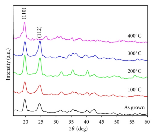
When XRD pattern of annealed thin films is studied, it is observed that the peak intensity and full width at half maxima (FWHM) of (110) and (112) planes increase. Hence enhancement in these peaks is the significance of postdeposition annealing treatment and indicates improvement in the crystallinity of the thin films. The average crystallite size of as grown and annealed thin films calculated using the Scherer formula is found to be 6.4, 7.1, 8.9, 10.6 and 11.2 nm, respectively [13]. This increase in crystallite size can be correlated to annealing-induced disorders in Ag-doped CdS thin films, as the large number of crystallites are present on the substrate, it is supposed that when annealing treatment is provided, the energy is absorbed by these crystalline, thereby they start coalescing with each other to form bigger crystallites, in other way it can be defined as melting and resolidification of crystallites which is called as polygonization. Therefore such high-energy induction reduces the strain in crystallites which is related to the structural deformations and disorders. Even upon annealing it is considered that the segregation of Ag+ ions may induce considerable distortion near the grain boundaries due to larger ionic radii of Cd2+ (0.151 nm) than Ag+ (0.122 nm) ions, therefore such distortion may provide route or space for fast mass transportation and growth of particle size [2, 14].
3.2. Raman Spectra
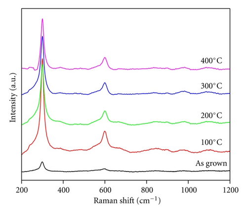
The annealing-induced modifications observed from XRD pattern can also be confirmed by Raman spectra, obtained from as grown and annealed Ag-doped CdS thin films as represented in Figure 2. From the figure, peak observed at ~303 cm−1 and 600 cm−1 represents Ag-doped CdS thin films, while upon annealing, enhancement in intensity and FWHM of these peaks are observed which may be related to material modifications and increase in the density of lattice defect in thin films [12]. These defect induces stress in thin film which became center for photo-generated charge trapping [13].
3.3. Compositional Analysis
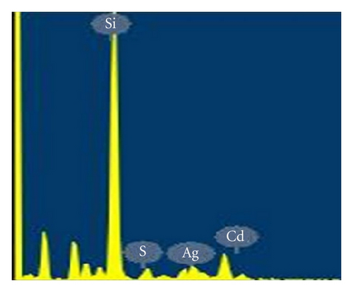
Figure 3 represents the energy dispersive X-ray (EDAX) spectra obtained from Ag-doped nanostructured CdS thin films for elemental composition analysis. The observation of peak corresponding to Cd, S, and Ag in the EDAX spectrum confirms Ag doping in CdS thin films, as such obtained elements confirm expected chemical composition in thin film.
3.4. Scanning Electron Microscopy (SEM)
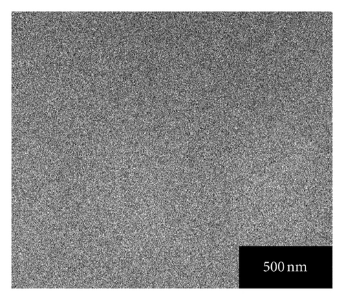
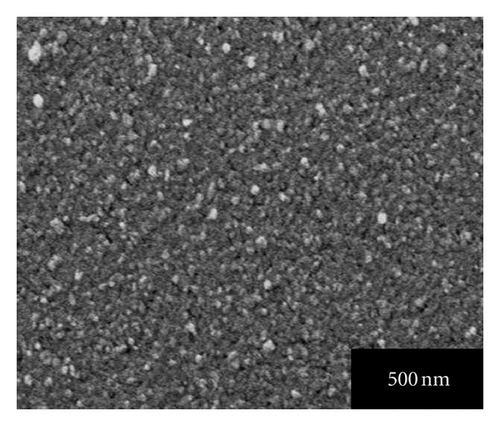
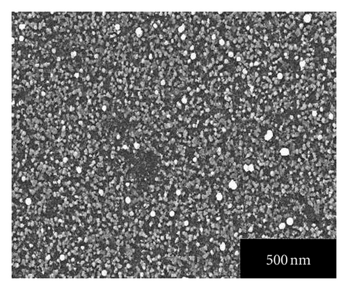
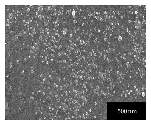
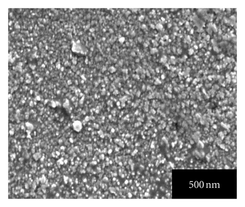
Figures 4(a), 4(b), 4(c), 4(d), and 4(e) represent the SEM images of as grown and 100, 200, 300, 400°C annealed, Ag-doped CdS thin films, respectively. From Figure 4(a) it can be seen that Ag-doped CdS thin films have uniform grain distribution over the substrate surface, as the annealing treatment is provided it starts expanding the grains in stages like in SEM image of 100°C annealed thin films, grains look like being expanded at their positions, for 200°C some grains melted down, for 300°C the grain boundaries are about to disappear to form bigger grains and finally at 400°C recrystallization occurs since polygonization process involves exchange of energy (absorption and desorption) by crystallite therefore by this phenomenon, the grains melt down by high energy and instantly it again resolidified to form larger grains. This could be related to the fact that the grains are made up of small grains which on providing the heat treatment may be coalescing thereby the grain boundaries melt down and these coalesced grains may unite together to form big grain. These large grains can be very useful since interface defect are associated with them which may enhance the performance by photo-generated charge trapping [15].
3.5. Optical Characteristics
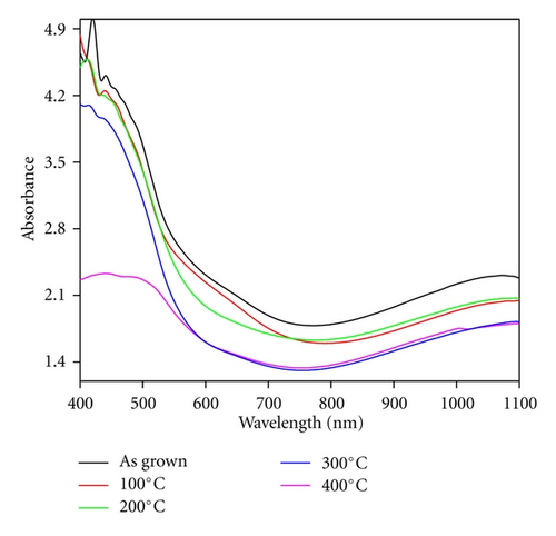
Annealing treatment to Ag-doped CdS thin films may affect the probable electronic transitions in the material which can be monitored by studying the optical properties of these thin films. Figure 5 represents the optical absorbance spectra of as grown and annealed Ag-doped nanostructured CdS thin films. From the Figure 5, it can be seen that the optical absorbance strength decreases as the annealing temperature is increased, may be due to variation in physicochemical properties such as crystallite size, surface morphology, and compositional modifications up to certain extent [15, 16]. Annealing provides possibility for ionic displacement in materials which can create large number of lattice defect like ionic vacancies, and so forth, these defect can act as trap centers and affect the optical absorbance. Therefore, decrease in optical band strength can be primarily associated with defect-induced band tailing due to creation of localized energy states near the band edge [17].
| Sr. No. | Sample | D (nm) | Eg (eV) | n (cm−3) | μ (cm2/Vs) | ρ (Ωcm) | S (%) |
|---|---|---|---|---|---|---|---|
| (01) | As grown | 6.4 | 2.28 | 5.7 × 10¹⁷ | 75.23 | 2.79 | 72 |
| (02) | 100°C | 7.1 | 2.23 | 9.2 × 10¹⁷ | 78.54 | 2.18 | 78 |
| (03) | 200°C | 8.9 | 2.21 | 4.3 × 10¹⁸ | 79.69 | 1.97 | 83 |
| (04) | 300°C | 10.6 | 2.18 | 8.1 × 10¹⁸ | 81.13 | 1.68 | 92 |
| (05) | 400°C | 11.2 | 2.14 | 6.3 × 10¹⁹ | 83.78 | 1.2 | 96 |
3.6. Electrical Measurements
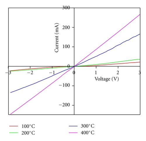
Annealing may significantly change the electrical properties, such as resistivity, charge carrier concentrations, and I-V response of the thin films. The density of charge carrier concentration in as grown and annealed thin films is calculated using Vander Pauw technique at room temperature under dark conditions. The density of carrier concentration and charge mobility are observed to be increased from 5.7 × 1017 cm−3 to 6.3 × 1019 cm−3 and 75.23 cm2/Vs to 83.78 cm2/Vs, while the electrical resistivity measured using two probe techniques is observed to be decreasing from 2.79 to 1.2 Ωcm for as grown to annealed thin films, respectively.
4. Conclusions
From the above study it can be concluded that the Ag-doped CdS thin films can be grown easily by simple, cost effective chemical route. The annealing treatment proves to be useful for physicochemical and optoelectronic modifications. XRD pattern shows an enhancement in crystallite size from 6.4 to 11.2 nm, Raman spectra confirms the material modification and SEM shows grain growth through polygonization process. Elemental composition analyzed using the EDAX confirms the stoichiometry of the thin film. Decrease in optical absorbance strength and energy band gap shows defect-induced charge transportations and the photosensitivity enhancement is observed from 72 to 96% upon annealing treatment. Finally it can be concluded that postdeposition treatment like air annealing helps in improving physicochemical as well as optoelectronic properties.
5. Research Highlights
-
Ag doping in nanostructured CdS thin films can be achieved by cost-effective chemical route.
-
Air annealing improves physicochemical and optoelectronic properties of these thin films.
-
400°C annealed Ag-doped CdS thin films improve photosensitivity from 72 to 96%.
Acknowledgments
The authors are thankful to The Head of Department of Physics, Dr. Babasaheb Ambedkar Marathwada University, Aurangabad for providing the laboratory facility and Dr. Anil V. Ghule, Assistant Professor, Department of Nanotechnology, Dr. Babasaheb Ambedkar Marathwada University, Aurangabad for helpful discussion.


