Scaling Considerations for Organic Photovoltaics for Indoor Applications
Abstract
Organic semiconductor-based photovoltaic (OPV) devices have many properties that make them attractive for indoor applications, such as tailorable light absorption, low embodied energy manufacturing and cost, structural conformality, and low material toxicity. Compared to their use as organic solar cells (OSCs) for standard outdoor solar harvesting, indoor OPV (IOPV) devices operate at low light intensities, and thus demonstrate different area-scaling behavior. In particular, it appears as though the performance of large-area IOPV devices is much less affected by the sheet resistances of the transparent conductive electrodes (a major limit in OSCs), but instead by factors such as their shunt resistance at low light intensities. Herein, the key parameters for improving the efficiency of large-area IOPV using drift–diffusion and finite element modeling (FEM) are examined. The scaling behavior at low-light intensities is theoretically and experimentally probed and demonstrated using the model PM6:Y6 system. The implications for the fabrication of large-area devices and the requirements for high shunt resistances for low-light performance are examined. These new insights present a clear route toward realizing monolithic large-area organic photovoltaic cells for indoor applications – which is a necessary technical step to practical implementation.
1 Introduction
Recently, indoor photovoltaics (IPV) have attracted intense research attention due to their potential in harvesting indoor light energy efficiently to drive low-power consumption electronic devices. This focus on IPV coincides with a period of accelerated advancement of low-power networked devices, many of which fall under the broad category of the “Internet of Things” (IoT). According to the Intel Corporation, there are already 200 billion such connected devices and 55% of all data, will be generated by IoT by 2025.[ 1 ] In the same year, the International Energy Agency (IEA) forecasts that the energy consumption of such devices is likely to reach over 1100 TWh yr−1 and recommends the adoption of smart solutions, such as energy harvesting, to avoid a large growth in electricity demand.[ 2 ] These devices are often designed with low power consumption in mind and may be used in ways in which providing a mains power supply would be impractical. Primary batteries may be suitable for some applications, but their routine replacement may be undesirable, uneconomical, and/or environmentally harmful.[ 3 ] The use of photovoltaics illuminated by indoor light is, therefore, an attractive option for the deployment of IoT devices in a “set and forget” fashion—in which embedded PV powers the device by harvesting the available light.
The suitability of various technological approaches to IPV has been the focus of many in-depth reviews.[ 4-14 ] These include silicon (Si: crystalline, polycrystalline, and amorphous), gallium arsenide (GaAs), copper indium gallium selenide (CIGS), and solution-processed approaches, such as dye-sensitized solar cells, perovskites, and organics.[ 4, 5, 8-11, 14-20 ] When comparing these technologies, there are a few notable differences in their optimization as IPV cells as compared to their solar equivalents.[ 13 ] First, the light incident on an IPV cell will have a much lower irradiance and a significantly different spectrum. The well-known theoretical maximum efficiency derived by Shockley and Queisser (SQ) – 33.7% for a single junction under AM1.5G conditions[ 21 ]––can be over 50% for a single-junction device under typical indoor illumination.[ 22 ]
The incident light spectrum changes the ideal energy gap for the PV system, as predicted by the SQ limit. Silicon, with a bandgap of 1.1 eV, is well suited for harvesting sunlight, but the longer wavelength onset is a source of radiative voltage loss, which lowers the cell performance considerably in indoor applications.[ 23 ] Higher band (energy) gaps (1.8–1.9 eV) are required to efficiently harvest light from indoor sources.
Another significant difference is that the typical operational conditions indoors are less severe than that in outdoor environments. Temperature and humidity fluctuations are more severe outdoors, which can significantly reduce the operational lifetime of a solar PV system.[ 24 ] This opens the door to thin-film PV technologies for IPV, as strategies for their use in solar PV are further optimized.[ 25 ] In addition to these physical factors, the market for low-cost PV modules for powering IoT devices makes solution-processable approaches more attractive. Other PV materials with a good spectral match for indoor applications may be too expensive for low-cost IoT applications (e.g., GaAs[ 15 ]) or may contain undesirable toxic materials (e.g., the lead-based perovskites[ 26 ]). Dye-sensitized solar cells have recently demonstrated promising ambient light performance[ 27 ] but questions remain as to the practicality of the liquid electrolyte which is a key component.
Of the contenders for low-cost IPV technologies, organic photovoltaics (OPV) are appearing to be particularly well-suited for use indoors (IOPV). Advantageous properties of OPV in embedded applications include compatibility with flexible substrates, low specific power, and favorable aesthetics.[ 28 ] As an emerging technology, OPV faces challenges in terms of cost and manufacturing scale when compared with other fully commoditized technology (such as the dominant incumbent crystalline silicon) in the mainstream solar energy market. Instead, application-targeted development of OPV leveraging their unique properties will likely pave the first paths to market as scalable fabrication processes are developed and the palette of available high-efficiency materials expands.[ 29 ]
Organic photovoltaics have been investigated for over three decades, during which time numerous materials and approaches have been developed to improve the relevant figures of merit.[ 30 ] Recent research focuses on non-fullerene acceptor (NFA)-based systems (the analogues to n-type inorganic semiconductors) have produced record-breaking figures of merit, including power conversion efficiencies (PCEs) of 19% under AM1.5G illumination.[ 31 ] Properties of NFA-based systems that contribute to these high efficiencies include high internal quantum efficiency (IQE), favorable phase morphologies, and low open-circuit voltage (V OC) losses.[ 32 ] For indoor applications, the wide optical gaps (>1.8 eV) and complementary acceptor/donor absorption make NFA-based systems competitive (if not superior) with/to other PV technologies. Common indoor illumination sources with emission in the visible band, for example, typical LED lights, have an emission onset at wavelengths of 700 nm[ 33 ] and PCEs of up to 30% have been reported for NFA-based systems under low-intensity incident LED lighting.[ 34 ] Rational design approaches to molecular synthesis have been successful in tuning the energy gap of a polymer donor-NFA blend to 1.84 eV, within the ideal range for indoor applications.[ 35 ]
Spectral matching to improve the conversion efficiency of incident indoor light to photocurrent is crucial in developing high-performance devices but minimizing recombination losses is another critical component of material choice. To this end, intensity-dependent measurements have been used to highlight the relative importance of Shockley–Read–Hall (SRH) and bulk bimolecular recombination processes at varying intensities and defect densities.[ 36 ] Analytical models have been put forward that aids the physical understanding of the relationship between fill factor (FF) and light intensity, and the role of tail states.[ 37 ]
In parallel with investigations into developing AL materials for IOPV, recent reports have included device-level optimizations. Simulation and experimental reports of IOPV devices have highlighted the importance of shunt resistance (R shunt), which should be sufficiently high to reduce the leakage current.[ 7, 38, 39 ] Critical values of R shunt of 1 MΩ cm2 and 85 kΩ cm2 have been reported, with others reporting the series to shunt resistance ratio (R series /R shunt), which was found to improve with AL thickness.[ 38, 40, 41 ] This has included reports of selecting the electron and hole transport layers (ETL/HTL) for IOPV. Polyaniline (PANI) doped with poly (4-styrenesulfonic acid) (PSS) has been demonstrated as an alternative to poly (3, 4-ethylene dioxythiophene) (PEDOT) as a more suitable HTL for indoor use, attributed to higher transmittance, work function, and device R shunt.[ 42 ] PDINO has been reported as a suitable ETL for IOPV devices due to its deep HOMO level, with reports of PCEs up to 31% under indoor lighting conditions.[ 34 ] For OPV devices with inverted architecture, the well-known phenomenon of “light-soaking”–in which pre-illumination of a device under test is required before the stable measurement of its FF––was reduced significantly by replacing zinc oxide (ZnO) with tin oxide (SnO2).[ 43 ]
The field of IOPV is showing impressive progress, with commercial activity already starting in this area.[ 35 ] However, many of the headline figures of merit for OPV devices are measured from small-area (<1 cm2) devices. At standard “1 sun” (AM1.5G) illumination, it is now well understood that the scaling of the cell area (i.e., maintaining small area performance to practical sizes) is predominantly limited by the performance of state-of-the-art transparent conductive electrode (TCE) materials.[ 44 ] However, at the low currents associated with IPV, the TCE contribution to the parasitic losses is negligible. Rather, it is the shunt resistance that determines the performance of IPV devices, particularly at low light intensities. This is usually quantified as a specific property – i.e., one that scales with device area.[ 38, 39 ] Therefore, one may project that low-cost monolithic IOPV modules may be produced by simply scaling the power densities measured for small-area devices to larger areas. But this assumption can be misleading for defect-dominated properties, such as the contribution of pinhole defects to R shunt, which are not deterministic. Further, to produce reliable output power, the maximum power point voltage (V MPP) behavior of IOPV systems is important to understand at its intended scale to embed IOPV modules with reliable energy harvesting circuitry.[ 8 ]
In this current work, the effect of scaling up the area of monolithic IOPV cells is investigated. Drift–diffusion simulations are based on the non-fullerene acceptor-based system, PM6:Y6, as the electro-optical properties are well reported for its use as a model system. Trends from these simulations are used to predict the behavior of idealized small-area devices under typical indoor illumination and review the relative importance of parasitic and recombination losses at varying light intensities. These results are interpreted using a two-diode equivalent circuit model that is used to highlight dominant loss mechanisms at varying light intensity. Finite element modeling (FEM) is then used to predict the performance metrics at larger cell areas, which matches those from small-area devices until a reversal point is observed. For practical IOPV devices, this reversal point should be below the practical indoor intensities found in typical indoor settings (50–1000 lux[ 22 ]), thus enabling the economic production of practical monolithic cells. As a critical variable for low-light performance, the scaling behavior of the specific shunt resistance is explored. Finally, exemplary thick-junction NFA-based OPV devices are measured under varying light conditions to demonstrate their applicability to IOPV applications.
2 Results and Discussion
2.1 Scaling of Cell Size at Low Light Intensities
When considering the use of OPV for a specific indoor application, the output power requirements and the incident light intensity must be carefully considered as primary design metrics. Idealized estimates of the minimum required cell sizes for IOPV applications are shown in Figure 1a. For typical IoT devices, the power requirements of the system will be dominated by their communication protocols.[ 8, 13 ] These may range from relatively simple radio frequency identification (RFID)- based devices (e.g., identification tags), requiring ≈10 μW, to more complex networked devices using Wi-Fi, which may have power demands on the order of 1 W.[ 8 ] The environment in which the device may be installed must also be considered, and in particular, the average light intensity incident on the device. From these idealized estimates, it is clear that the cell sizes required to enable IoT applications in realistic scenarios will consistently require cell sizes >5 cm2, substantially larger than the typical lab-scale areas used to report performance metrics of OPV systems.
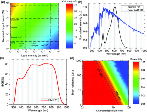
The spectral properties of the incident light typical of indoor environments must also be considered when optimizing IOPV systems. Figure 1b shows the normalized intensities for an AM1.5G spectrum and a typical 2700 K LED. It should be noted that photometric units are typically used for lighting applications (e.g., the measurement of illuminance in lux), whereas the light intensity (irradiance) calculated from the integrated radiometric spectrum may differ significantly, depending on the light source.[ 45 ] When developing material systems for IOPV, one must consider the spectral match to the incident light. Figure 1c shows a typical external quantum efficiency (EQE) spectrum for PM6:Y6, which is used here as a prototypical NFA-based system. Other NFA systems have been reported that provide a more suitable spectral match to indoor light sources.[ 35 ]
For OSC applications, the Ohmic losses associated with the series resistance of the transparent conducting electrode (TCE) will typically dominate the performance of a large-area monolithic cell. Here, we use the term monolithic to indicate that the light-harvesting area of the cell is a single structure rather than serially interconnected thin strips – the latter being the predominant, complex, costly, and rather limiting architecture used in OPV manufacturing today, with the former being by far the most attractive alternative akin to how c-Si modules are assembled. However, at light intensities significantly below 1 Sun such as those relevant to indoor applications, the lower photocurrent () will have much lower associated Ohmic losses through the TCE, as when , where is the photocurrent of an OPV device under indoor illumination and is the photocurrent under 1 Sun. Figure 1d shows estimates of scalability at 0.01 Sun, and the equivalent plot under 1 Sun is provided in Figure S1, Supporting Information, with varying characteristic size and TCE sheet resistance. The scalability is calculated using a simple 1D model explained in the previous work[ 46 ] for monolithic OPV devices with no serial connections included, with Ohmic losses from the TCE calculated across the characteristic length (see Supporting Information for calculational details). While at high intensity, a desirable 90% scalability can only be achieved for devices smaller than 1 cm (assuming typical indium tin oxide (ITO) TCE sheet resistance of 10 Ω □−1), at low intensities, relevant to IOPV, characteristic sizes on the order of 10 cm can be accommodated with acceptable scalability. Further, the use of brittle (and expensive) metal oxides such as ITO (R sheet = 10–20 Ω □−1) may not be necessary for IOPV optimal performance, and other solution-processable TCE materials with larger R sheet (≈100 Ω □−1) may be sufficient for these applications, and TCE materials may be selected for other parameters such as work function and low surface roughness.[ 42 ] This difference in device scalability at lower light intensities can enable ITO-free devices and TCEs deposited on flexible substrates processed at low temperatures.
2.2 Small Area Devices: Drift–Diffusion Model
A drift–diffusion model was used to investigate the intensity-dependent performance of small-area devices with the structure: ITO/PEDOT/PM6:Y6/PDINO/Ag (described in Materials and Methods, below). To account for optical interference effects, an optical transfer-matrix model was used to simulate the charge generation rate inside the active layer. Figure 2 highlights the various contributions to the loss of FF (left axes, solid lines) and PCE (right axes, dashed lines) under illumination from a 2700 K LED source with varying light intensity. The default parameters assumed for the small-area PM6:Y6 device are: an active layer thickness of d = 90 nm, electron and hole mobilities of 1.2 × 10⁻³ and 2 × 10⁻⁴ cm2 V−1 s−1, respectively[ 47 ] and a bimolecular recombination coefficient reduction factor of relative to the Langevin rate constant.[ 48 ] Furthermore, unless otherwise stated, the presence of SRH recombination via mid-gap trap states in the active layer having an SRH carrier lifetime of ; a shunt resistance of R shunt = 106 Ω cm2 ; and an external series resistance of R series = 0 Ω cm2 are assumed in the small-area device.
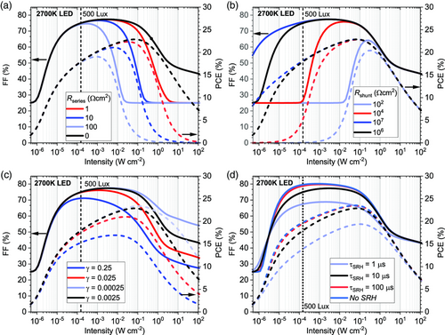
The effect of nonzero series resistance and varying R shunt is shown in Figure 2a,b, respectively. In general, the intensity dependence of the FF and PCE can be separated into three different regimes. The losses caused by a nonzero series resistance dominate only for high-light intensities, at which point small differences in series resistance contribute to large losses in the PCE, while the FF decreases to 25%. In contrast, losses induced by a finite R shunt generally dominate at low-light intensities. In this regime, the FF decreases rapidly and saturates again at 25%, while the PCE decreases linearly with the short-circuit current density J sc (since in this limit), becoming negligibly small at low light intensities.
Finally, at moderate intensities, the PCE and FF are determined by the recombination of photogenerated carriers in the device. Figure 2c,d show the corresponding contributions of recombination losses at varying light intensities, considering the effect of bimolecular recombination reduction factor γ and SRH lifetime , respectively. In the case of negligible bimolecular recombination () the FF varies only marginally with light intensity as a result of reduced recombination, reducing the losses even at high intensities. As γ is increased, the FF decreases at higher intensity due to the more pronounced effect of nonlinear bimolecular recombination, with the FF eventually dropping rapidly at higher light intensities. At lower light intensities, the FF becomes insensitive to the light intensity and instead is limited by first-order SRH recombination, with a decrease in SRH lifetime correlating with a reduced FF; while at very long lifetimes (), the associated losses are negligible.
In the recombination-dominated intensity regime, the PCE is seen to generally decrease with decreasing intensity at the lower intensities. Noting that where P in is the incident light intensity and , it becomes evident that the decrease in PCE is predominantly due to the drop in V OC of the cell, scaling with intensity as in this case ( = thermal voltage, is the ideality factor).
In this regard, the use of equivalent circuit models can provide further insight into the operation of IOPVs at low-light intensities before specific material system parameters are considered.[ 49 ] The open-circuit voltage derived from the drift–diffusion simulations at different intensities is displayed in Figure 3a. The open-circuit voltage is approximated well by a two-diode model (Figure 3a, inset), as outlined in previous work,[ 50 ] which considers the current contributions from bimolecular recombination (j 1), and recombination via trap states (j 2). For devices with sufficiently high R shunt, a plot of V OC with varying light intensity can be used to identify regions where each of these equivalent diodes dominates. The main plot seen in Figure 3a shows the simulated V OC behavior of the PM6:Y6 system outlined in the previous section at two active layer thicknesses (90 nm—blue curve, 200 nm—red curve). Fitting the respective ideality factors for diode 1 (n id = 1) and diode 2 (n id = 2) reveals a gradual transition between the two regions. The associated power conversion efficiencies are plotted in Figure 3b.
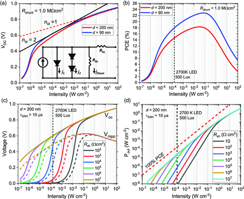
With R shunt < 105 Ω cm2, the drop in both V OC and the maximum power point voltage (V MPP, dashed lines) is significant at typical indoor light intensities. The associated maximum power point tracking circuit required to charge batteries (or capacitors) for any stand-alone power system would therefore need to accommodate these large variations. A more gradual drop in V OC/V MPP is given by values of R shunt > 106 Ω cm2, which is more practical for embedded IOPV systems with simpler external circuitry. The associated maximum power per area with varying light intensity estimated with different R shunt is shown in Figure 3d. While the maximum power scales linearly with the intensity at large R shunt (corresponding to the recombination-dominated intensity regime), a quadratic intensity dependence () is seen at small shunt resistances, resulting in large losses. For viable IOPV-integrated devices, it is critical that sufficient voltage and power is delivered to the associated charging or load circuitry.
2.3 Large-Area Devices: Finite Element Model
The performance of large-area devices was investigated using 2D finite element models, extending the small-area models detailed in the previous section and corresponding to typical output power requirements for IoT applications. The comparison between the small (dashed lines) and large-area (solid lines) device performance with varying light intensities is shown in Figure 4 . The linear behavior of J sc with light intensity (Figure 4a) deviates at higher intensities – this inflection point is determined by the cell size. This is of practical importance if using J sc as a means of estimating the light intensity incident on a real cell – underestimates may occur with large-area devices measured at high light intensities. The effect on V OC and V MPP is shown in Figure 4b. As no Ohmic losses occur when J = 0, V OC is unchanged by the scale of the cell. However, V MPP is seen to deviate from the small area significantly at larger cell sizes.
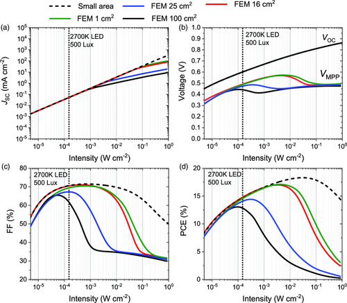
The loss of FF (Figure 4c) is exacerbated at higher light intensities (>10−2 W cm−2), with the loss of PCE (Figure 4d ) consistently below that of the small-area device. It should be noted that real devices may suffer from further Ohmic loss terms associated with lead resistances at higher currents, not considered in this model. It should be emphasized that in this model, the specific shunt resistance is kept constant with varying cell sizes. This assumption is examined for real devices in the next section.
2.4 Variation of Shunt Resistance in NFA-Based OSCs
Thin films formed from solution-processed PV materials such as OPVs are known to contain defects that contribute to the overall R shunt.[ 44 ] As R shunt is a crucial parameter in determining the performance of NFA-based OSCs at low-light intensities, its variation with respect to active layer thickness and cell size are key factors for IOPV applications. The variation of R shunt for solution-processed layers is explored in Figure 5 . Specific shunt resistances measured from two related NFA-containing blends, PM6:Y6 and PM6:BTP-eC9 (described in the Experimental Section, below) with varying active layer thickness and are shown in Figure 5a,b. The trend of higher shunt resistances with increasing junction thickness will generally hold in the regime where the morphology of the active layer does not change substantially at different thicknesses. The morphology of each blend will also have an impact on the leakage currents, which will have influences from the solubility of the materials, the crystallinity of the film, and the molecular order. Between these two blends, BTP-eC9 has a higher solubility, which may contribute to the tendency to produce devices with higher R shunt. The trend toward higher R shunt with thicker active layers is thus not deterministic, especially in devices that may have point defects from fabrication which are randomly distributed as is the case for solution processing.
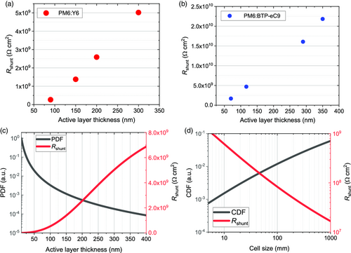
An illustrative example of this distribution is shown in Figure 5c, where its inverse is proportional to R shunt. This illustrative model highlights the requirements for thicker active layers in the creation of IOPV devices to mitigate the impacts of point defects.
2.5 Measurement of PM6:Y6 Devices with Varying Light Intensity
Devices based on the NFA system PM6:Y6 (≈200 nm thick, see Methods) were fabricated and measured with varying intensities of an LED light source. The input light intensity was calculated using the EQE of the device and checked against a reference photodetector (see Supporting Information for full details). The figures of merit obtained from three exemplary pixels are shown in Figure 6 . Several pixels on the same sample were measured, the largest of which (1 cm2), had a comparable shunt resistance (≈1 GΩ cm2) to a smaller pixel (0.15 cm2 ). Another small pixel (0.15 cm2) with a lower shunt resistance was measured for comparison (≈100 MΩ cm2). The resulting FF is plotted in Figure 6a. Under high-intensity AM1.5G illumination (Figure S12, Supporting Information), the small-area pixels had a higher FF than the large-area pixel, consistent with the larger Ohmic losses. However, under LED illumination, the situation reverses – the pixels with comparable high R shunt perform similarly at low intensities, and the performance of the low-shunt pixel falls rapidly at low intensities, consistent with the simulation in this and other works.[ 11, 20, 52 ]
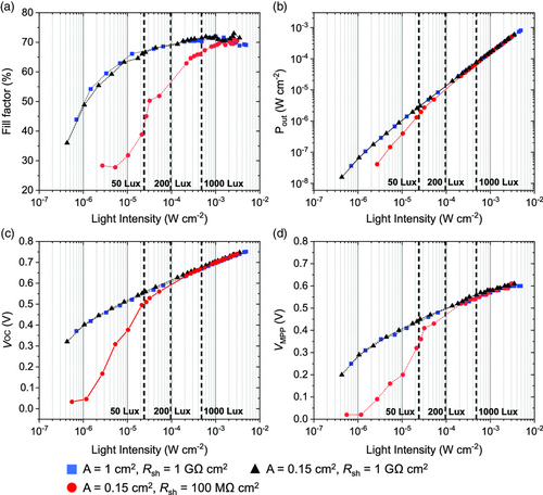
This is also highlighted in the trends of V OC and V MPP, shown in Figure 6c,d. At light intensities below 10−4 W cm−2 (≈200 Lux), the V MPP of pixel with R shunt = 100 MΩ drops rapidly.
2.6 Technological Perspective
The issue of the area scaling of OSCs – designed to operate at or around 1 Sun – is a technical challenge, but one that is parametrizable.[ 53 ] Materials can be optimized to reduce recombination losses, and TCEs can be developed, for example, with metallic grids, to reduce its R sheet and improve its scalability and flexibility.[ 54, 55 ] In comparison, the development of IOPV is a multivariate problem – which is inherently application-specific, and a systems-integrated approach is necessary to fully realize the potential of OPVs for these applications.
First, the incident light spectrum and power on an IOPV system may not be easy to predict. Systems could be installed in locations where combinations of natural and artificial light may be present, and vastly different depending on the time of day, season, room occupancy, and other factors.
Both simulation results and device measurements presented in this work highlight the importance of shunt resistance for low-light applications. Particularly for solution-processed materials (which many organic semiconductors are), the stochastic nature of defects leading to low shunts precludes a fully deterministic optimization for their use in IOPV. However, from illustrative models, we can point toward general trends that will improve device performance. The use of thick (>100 nm) active layers and high-quality, planar TCE structures will tend to reduce the prevalence of point defects. Encouragingly, many NFA-based systems reported in the recent literature perform well with thick active layers (>>100 nm), suggesting that suitable large-area (and indeed monolithic) structures may be solution-processable using scalable techniques. The choice of active layer thickness presents an optimization problem between the maximum attainable PCEs of thinner films (<100 nm), and the consistency of low-light performance from devices that are not shunt-limited from point defects. The choice of deposition methods of the constituent layers of IOPV devices will play a critical role in determining its applicability to the production of large-area monolithic cells. Blade-coated devices have been demonstrated as outperforming their spin-coated counterparts at low light (200 lux) reports by Cui et al.[ 35 ] The use of lamination techniques is another promising coating technique, as reported for semitransparent flexible OPV and organic photodetectors.[ 56, 57 ]
3 Conclusions
The use of NFA-based OPV devices under low-light intensities such as in indoor settings has been examined through theory, simulation, and experimental verification. Drift–diffusion, equivalent circuit, and finite element models were used to investigate the effect of scaling cell areas to larger dimensions to produce sufficient power for IoT-type applications. Exemplary devices based on the NFA system PM6:Y6 were measured under varying light intensity.
In comparison to the scaling of OSCs at high light intensities (i.e., at or near 1 Sun), IOPV is not limited by the series resistance of the TCE, but rather material and device properties such as low shunt resistance, and first-order recombination losses such as SRH recombination. Thus, the development of organic semiconductor PV materials for indoor applications must also consider the prevalence of point defects in the films and other morphological contributions to low shunt resistance in a cell. The development of films for these applications will no doubt enable the use of OPV for indoor applications and provide a viable route to large-scale production in general. Application-targeting of OPV provides a parallel and maybe more immediate and tangible route to commercial uptake relative to standard stationary solar power.
4 Materials and Methods
4.1 Materials
BTP-eC9: 2,2'-[[12,13-Bis(2-butyloctyl)-12,13-dihydro-3,9-dinonylbisthieno[2'',3'':4',5']thieno[2',3':4,5]pyrrolo[3,2-e:2',3'-g][2,1,3]benzothiadiazole-2,10-diyl]bis[methylidyne(5,6-chloro-3-oxo-1H-indene-2,1(3H)-diylidene) ]]bis[propanedinitrile]
PDINO: 2,9-bis[3-(dimethyloxidoamino)propyl]anthra[2,1,9-def:6,5,10-d′e′f′]diisoquinoline-1,3,8,10(2H,9H)-tetrone
PEDOT:PSS: Poly(3,4-ethylenedioxythiophene) polystyrene sulfonate
PM6: Poly[(2,6-(4,8-bis(5-(2-ethylhexyl-3-fluoro)thiophen-2-yl)-benzo[1,2-b:4,5-b′]dithiophene))-alt-(5,5-(1′,3′-di-2-thienyl-5′,7′-bis(2-ethylhexyl)benzo[1′,2′-c:4′,5′-c′]dithiophene-4,8-dione)]
Y6: 2,2′-((2Z,2′Z)-((12,13-bis(2-ethylhexyl)-3,9-diundecyl-12,13-dihydro-[1,2,5]thiadiazolo[3,4-e]thieno[2′′,3′′:4′,5′]thieno[2′,3′:4,5]pyrrolo[3,2-g]thieno[2′,3′:4,5]thieno[3,2-b]indole-2,10-diyl)bis(methanylylidene))bis(5,6-difluoro-3-oxo-2,3-dihydro-1H-indene-2,1-diylidene))dimalononitrile
PM6, Y6, BTP-Ec9, and PDINO were purchased from Solarmer (Beijing). PEDOT:PSS was purchased from Heraeus (Germany)
4.2 Drift–Diffusion Simulations
For the drift–diffusion simulations, a combined electrical-optical device model was used.[ 48 ] In the model, the Poisson equation and the continuity equations for electrons and holes are numerically solved using Gummel's iteration method and the Scharfetter–Gummel discretization scheme.[ 58 ] The corresponding electron and hole current densities in the active layer are described by the drift–diffusion relations. The active PM6:Y6 layer is treated as an effective semiconductor with an energy level gap of 1.22 eV, where holes (electrons) are transported in the valence (conduction) level of PM6 (Y6). Corresponding electron and hole mobilities of 1.2 × 10⁻³ and 2 × 10⁻⁴ cm2 Vs−1 are assumed, while equal effective densities of states of 1020 cm−3 are considered. Furthermore, the Einstein relation between the mobility and the diffusion constant is applied. In addition, the contacts are assumed to be nonselective, with injection barriers of 0.1 eV for the majority carriers. The recombination rate of free charge carriers in the bulk is assumed to be composed of both bimolecular recombination and SRH recombination via mid-gap traps. The generation rate of electrons and holes is further calculated using an optical transfer matrix model, which accounts for interference effects,[ 59 ] assuming the following device structure: Glass/ITO/PEDOT/PM6:Y6/PDINO/Ag. Based on the above assumptions, the model then calculates the steady-state device current density as a function of the voltage drop across the device. Finally, after accounting for a finite shunt resistance () and nonzero series resistance (), the output (external) current density–voltage (J-V) curve is obtained from and .
4.3 Finite-Element Simulations
Finite-element simulations were performed using LAOSS software (Fluxim AG), with input small-area JVs calculated in the method outlined in the previous section. 4 cm × 4 cm cells were simulated with a TCE resistance of 15 Ω □−1. Boundary conditions were set such that the sides of the simulated cell were at equal potential.
4.4 Fabrication of PM6:Y6 OPV Devices
PM6:Y6 devices with varying junction thickness were fabricated with a conventional structure (ITO/PEDOT: PSS/PM6:Y6/PDINO/Ag). PEDOT: PSS solution was first diluted with the same volume of water and then cast at 4000 rpm on ITO substrates followed by thermal annealing at 155 °C for 15 min to form a 10 nm film. PM6:Y6 was dissolved in a CF:CN (99.5:0.5) solution with a donor: acceptor ratio of 1:1.2 by weight. The thicknesses of PM6:Y6 films were adjusted by changing the concentration of the solution and the spin coating speed −35 mg mL−1 CF:DIO solution with 4000 rpm for 310 nm, 25 mg mL−1 CF:DIO solution with 4000 rpm for 190 nm, 20 mg mL−1 CF:DIO solution with 4000 rpm for 160 nm, 16 mg mL−1 CF:DIO solution with 2000 rpm for 109 nm. The active layers were further thermally annealed at 100 °C for 10 min. Afterward, 1 mg mL−1 PDINO solution was spin-coated on PM6:Y6 films at 2000 rpm to form 10 nm films, and 100 nm of Ag was evaporated as the top electrode.
4.5 Fabrication of PM6:BTP-eC9 Devices
PM6:BTP-eC9 devices were fabricated with a conventional structure (ITO/PEDOT:PSS/PM6:BTP-eC9/PDINO/Ag). PEDOT:PSS solution was first diluted with the same volume of water and then cast at 4000 rpm on ITO substrate and followed by thermal annealing at 155°C for 15 min to form a 10 nm film. PM6:BTP-eC9 was dissolved in a CF:DIO (99.5:0.5) solution with a donor: acceptor ratio of 1:1.2 by weight. The thicknesses of PM6:BTP-eC9 films were adjusted by changing the concentration of the solution and the spin-coating speed −35 mg mL−1 CF:DIO solution with 2000 rpm for 340 nm, 30 mg mL−1 CF:DIO solution with 2000 rpm for 293 nm, 16 mg mL−1 CF:DIO solution with 3000 rpm for 90 nm, 12 mg mL−1 CF:DIO solution with 3000 rpm for 60 nm). Afterward, 1 mg mL−1 PDINO solution was spin-coated on PM6: BTP-eC9 film at 2000 rpm to form 10 nm films, and 100 nm of Ag was evaporated as the top electrode.
4.6 Fabrication of Exemplary PM6:Y6 Devices with Varying Size
PM6:Y6 devices were fabricated on ITO/glass substrates. The device layout comprised a single 1 cm2 pixel and five 0.15 cm2 pixels. The device structure was as follows: glass/ITO/PEDOT:PSS/ PM6:Y6 (≈220 nm)/PDINO/Ag.
4.7 Measurement of PM6:Y6 Devices
Measurement of OPV devices was first performed under AM1.5G illumination (Oriel LCS-100), calibrated using a reference Si cell (Newport 91150 V). JV profiles were measured using a Keithley 2400 source/measure unit, controlled via a custom LabVIEW script. Standard 1 Sun and dark JV profiles were recorded before subsequent measurements. Attenuated AM1.5G spectra were obtained by varying the shutter on the lamp source and confirming the output power via the reference Si cell. All JV measurements were performed using a shadow mask.
For LED illumination, a bare LED bulb was driven using a constant current source (Keysight E364A). Light intensity was varied by moving the device under test from the LED source using a sliding stage (Autolab). JV profiles were measured at each intensity. Current from a reference photodiode (Thorlabs SM1PD1) was measured using a separate Keithley 2450 source/measure unit. JV profiles were analyzed using a custom script.
Acknowledgements
This work was supported by the Welsh Government's Sêr Cymru II Rising Star and Capacity Builder Accelerator Programs through the European Regional Development Fund, Welsh European Funding Office, and Swansea University Strategic Initiative in Sustainable Advanced Materials. A.A. is a Sêr Cymru II Rising Star Fellow and P.M.is a Sêr Cymru II National Research Chair. This work was also funded by UKRI through the EPSRC Program Grant EP/T028511/1 Application Targeted Integrated Photovoltaics.
Conflict of Interest
The authors declare no conflict of interest.
Open Research
Data Availability Statement
The data that support the findings of this study are available from the corresponding author upon reasonable request.


