Toward Understanding the Short-Circuit Current Loss in Perovskite Solar Cells with 2D Passivation Layers
Abstract
Herein, a strong short-circuit current density (JSC) loss is observed when using phenetylammonium iodide (PEAI) as n-side passivation in p–i–n perovskite solar cells. Comparing experiments with drift–diffusion simulations, different hypotheses for the origin of the JSC loss are presented and evaluated. Whereas the optical properties of the investigated cell stack remain unchanged, the internal quantum efficiency of the PEAI-based devices decreases drastically. Strong bulk doping and interface traps are ruled out as the origin of the charge extraction limitation. High-spatial resolution photoluminescence (PL) spectroscopy directly images the inhomogeneity of the PEAI-based quasi-2D perovskite wide-bandgap interlayer, which is found to be crucial for the observed JSC loss. A 2D drift–diffusion model implemented with mobile ions and an inhomogeneous electron transport layer reproduces the experimental behavior accurately. The ionic space charge distribution under short circuit reduces the effective charge-carrier diffusion length, hindering charge transport toward those domains in the perovskite–electron transport layer interface where electrons can be extracted efficiently. A longer charge-carrier lifetime reduces the JSC loss, highlighting the importance of suppressed non-radiative bulk recombination, not only for achieving high open-circuit voltages, but also for efficient charge extraction.
1 Introduction
In recent years, organic–inorganic perovskite solar cells became one of the most promising and most studied technologies in third-generation photovoltaics. Impressive efficiencies of up to 25.7% have been reached already, surpassing record efficiencies for well-established technologies like copper indium gallium selenide solar cells (CIGS) (23.4%) or multi-crystalline silicon solar cells (23.3%).[1] Recent studies predict a fundamental efficiency limit of perovskite single junction solar cells to be higher than 30%.[2, 3] To push efficiencies in this direction, light management and minimization of non-radiative losses are identified as main pathways. Light management can boost the absorption, majorly increasing the short-circuit current of the solar cell.[4-6] The suppression of non-radiative recombination will be foremost reflected by an increase of the open-circuit voltage (VOC).[7-10] For this aim, additives in the perovskite precursor such as methylenediammonium dichloride (MDACl2), formamidine formate (FAHCOO), or 1-butyl-3-methylimidazolium tetrafluoroborate (BMIMBF4) have been successfully introduced.[11-13] In addition, the optimization of charge transport layers (CTLs) can have a strong contribution to the suppression of interfacial recombination.[14-16] For further interface modification, recent approaches employ materials that induce the growth of a quasi-2D perovskite on top of the 3D perovskite bulk, for example, n-butylammonium bromide (n-BABr), phenetylammonium iodide (PEAI), phenetylammonium chloride (PEACl), or 4-tert-butyl-benzylammonium iodide (tBBAI).[17-21] Using the aforementioned passivation strategies often means balancing on the small ridge between the desired performance increase and unwanted losses introduced by additional layers or additives, which is often manifested in a reduction of the short-circuit current density (JSC) of the solar cells. Amino acid additives can for example introduce a significant loss in JSC attributed to inefficient charge extraction.[22-24] Choosing a highly doped transport layer can increase surface recombination and lower the VOC as well as the JSC.[25] The low relative permittivity of organic transport layers could possibly lead to a shielding of the built-in field and thus lower the driving force for charge carriers in the perovskite bulk, ultimately reducing charge extraction.[26] In addition to the mentioned losses induced by bulk or interface modifications, a recent study identifies ionic space charges as the origin of transient current loss in perovskite solar cells.[27, 28] Photoluminescence (PL) measurements are a powerful tool to gain insight in the mechanism behind current or voltage losses, and especially the PL quenching between open-circuit (OC) and short-circuit (SC) condition of complete solar cells is an important measure to quantify charge extraction properties.[24-27, 29, 30] It seems paradox that this quenching analysis is often transferred to the steady-state PL characterization of bilayer systems (perovskite/CTL).[31-34] It is evident that a decreased steady-state PL intensity in such a bilayer system can only be due to additional non-radiative recombination.[16, 35] Nevertheless, as perovskite solar cells are often governed by interfacial recombination, the PL intensity can remain high due to transport limitations.[36-38] In this work, we investigate high-efficiency perovskite solar cells in p–i–n configuration with a PEAI-based 2D passivation layer as model system. With increasing thickness of the PEAI layer, an increased JSC loss is observed, while the fill factor (FF) is much less affected. In the following, a comprehensive study, connecting experiments and drift–diffusion simulations, is presented to explain this behavior and demonstrate how bulk recombination limits the JSC.
2 Theory
As Jr is proportional to the emitted PL intensity of the solar cell, cex can be experimentally determined by PL measurements.
3 Results and Discussion
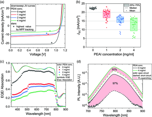
This study is based on perovskite solar cells with a mixed-cation mixed-halide lead-based perovskite Cs0.05MA0.10FA0.85Pb(I0.95Br0.05)3 absorber layer in planar p–i–n architecture with the following layer stack: indium tin oxide (ITO)/[2–(3,6–dimethoxy–9H–carbazol–9–yl)ethyl] phosphonic acid (Meo-2PACz)/perovskite/phenethylammomium iodide (PEAI)/[6,6]-phenyl-C61-butyric acid methyl ester (PCBM)/bathocuproine (BCP)/aluminum (Al). The layer structure is shown in Figure S1, Supporting Information; and details of the device fabrication can be found in Experimental Section. With this architecture, we regularly achieve power conversion efficiencies of 20% in our lab under simulated AM1.5G (1 sun) illumination. Figure 1a shows that with an increased concentration of the PEAI solution applied for perovskite passivation on the n-side, the JSC is decreased drastically while the VOC increases. It is remarkable that the FF does not decrease proportionally to the short-circuit current loss and stays rather constant. The steady-state power output during maximum power point tracking also decreases with increasing PEAI concentration. A meaningful statistical representation of the JSC can be found in Figure 1b, the statistics of other solar cell performance parameters are given in Figure S2, Supporting Information. With increasing PEAI concentration, it is expected that the mean thickness of the quasi-2D perovskite layer increases. With the used concentrations ranging from 0 to 4 mg mL−1 PEAI in isopropanol, however, the layer thickness is too thin to be measured in scanning electron microscope (SEM) cross-section images (compare Figure S3a, Supporting Information). Figure S4a, Supporting Information, shows the PL spectra of perovskite layers passivated with PEAI. The two peaks indicate that there are wide-bandgap semiconductors (bandgap energies from PL 2.4 and 2.2 eV) being formed on top of the 3D perovskite bulk material with a shift in bandgap depending on the composition of the quasi-2D Ruddlesden–Popper perovskite (3D perovskite peak around 800 nm, respectively 1.55 eV, not shown).[39] Figure S5b, Supporting Information, reveals that the additional layer leads to two new reflexes in X-ray diffractograms. In the following paragraphs, the short-circuit current loss with increased PEAI concentration will be analyzed and its origin will be discussed.
3.1 Optics
A simple explanation of a reduction in JSC would be the reduction of Jgen in Equation (1). In general, thin-film optics and interference important factors for light absorption and emission in thin-film solar cells.[40] However, for the case presented in this work, Figure 1c proves that the light absorption of the solar cell is not changed when increasing the PEAI concentration. As the passivation layer is a very thin, wide-bandgap semiconductor layer on the backside of the perovskite absorber layer, it cannot induce noticeable parasitic absorption. Comparing the external quantum efficiency (EQE) measurements to the absorption measurements, it is evident that the JSC loss is not due to a change of optical properties.
3.2 Charge Extraction
With unchanged optics between the varying PEAI concentrations, the difference of the EQE measurements of the passivated devices (red, blue, green symbols in Figure 1c) to the non-passivated device (black symbols) gives the fraction of charge carriers lost due to the passivation layer. PL-quenching measurements shown in Figure 1d specify how the charge carriers are lost. The solid lines depict the PL measurements in open-circuit condition. The device with PEAI passivation layer shows a PL peak intensity that is roughly one order of magnitude higher than for the non-passivated sample. This fits to the steady-state VOC difference measured simultaneously, which is 60 mV and indicates that the PEAI treatment has indeed the desired passivating effect. The PL measurements in short-circuit condition (dashed lines) allow to determine the charge extraction coefficient of Equation (2), which is 50% for the passivated and 97% for the non-passivated device, respectively. This is fully in line with the roughly 50% short-circuit current reduction that is observed in simultaneous JSC measurements. Even though the PEAI treatment is supposedly just a surface modification, the charge carriers are lost due to recombination in the perovskite bulk.
3.3 Asymmetric Low Charge-Carrier Conductivity
Normalizing the EQE measurement presented in Figure 1c (compare Figure S6, Supporting Information) reveals that, for the passivated solar cells, charge extraction is impeded disproportionately strong in the short-wavelength regime. Due to the larger absorption coefficient of high-energy photons, they are being absorbed rather in the front of the solar cell, close to the hole contact, whereas for lower-energy photons, the absorption is more homogeneous. It can thus be hypothesized that electrons generated in the front of the device are retained from reaching the back contact under short-circuit conditions. This could be caused by a low electron conductivity in the photoactive layer, for example, due to strong p-doping or a large negative space charge close to the electron contact. Simulated JV-curves for the models of bulk doping and recombination inactive traps at the perovskite/electron transport layer (ETL) interface that reproduce the experimental current–voltage behavior can be found in Figure S7, Supporting Information. In both cases, the low electron conductivity leads to an accumulation of electrons in the bulk perovskite already under short-circuit conditions and hence increases radiative as well as non-radiative recombination in the bulk. The two models can be validated by additional measurements. Namely, a high doping density (around 1018 cm−3 for 50% JSC reduction) of the bulk perovskite would lead to a large number of free charge carriers in the dark at 0 V. Charge extraction by linearly increasing voltage (CELIV) measurements would reveal this strong doping by a higher charge extraction signal. In Figure 2a, the CELIV measurements are shown for a device without (solid) and with (dashed) PEAI passivation. The dark curves are completely identical and there is no sign of an extraction peak. This disproves the hypotheses that the JSC loss could stem from a large bulk doping in the order of 1018 cm−3. The photo-CELIV curves measured at different excitation intensities (this allows for a rough estimation of the sensitivity of the CELIV measurement) show a lower peak height and a slower charge extraction for the solar cell with PEAI passivation.
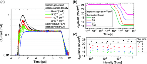
Regarding interface traps, simulations indicate that the short-circuit current reduction shows a time dependence and intensity dependence as depicted in Figure 2b. Upon starting a constant illumination, the current would have a high initial value and starts to decrease when the interface traps are being filled. This contradicts the experimental observation depicted in Figure 4c where upon starting illumination (at t = −30 s) the current output rises from a low initial value. Furthermore, regarding interface traps, the magnitude of the JSC loss should depend on the illumination intensity. Figure 2c shows intensity-dependent JSC for devices with different PEAI concentration. The magnitude of steady-state JSC reduction due to PEAI passivation is rather constant over the measured range of illumination intensities with only a slight tendency toward a lower impact under low intensities. These findings thus exclude that a space charge from trapped electrons is the major cause for the JSC loss due to PEAI passivation.
3.4 Homogeneity of the 2D Perovskite Interlayer
2D or quasi-2D perovskite materials are known to have worse charge transport properties than their 3D counterparts.[41] However, just the transport properties of the 2D passivation layer cannot explain the large JSC loss with simultaneously rather constant FF. This is illustrated by Figure S8a, Supporting Information, which shows drift–diffusion simulations of a device with varying electron mobility in the 20 nm thick ETL. The FF is affected well before the JSC by decreasing transport layer mobility and in this example falls below 25% in the case of reduced JSC. In literature, PEAI has been successfully employed as p-side passivation layer as well as n-side passivation layer.[18, 42, 43] This is somewhat puzzling, as the resulting 2D perovskite layer should lead to a band offset for the majority charge carrier in at least one of the cases. As depicted in Figure S9, Supporting Information, in our experiments, the PEAI passivation leads to a slight VOC increase with negligible JSC loss in the n–i–p configuration (i.e., when employed as a p-side passivation), whereas it induces a large JSC loss when employed as n-side passivation in the p–i–n configuration. Ultraviolet photon spectroscopy (UPS) measurements (Figure S5a, Supporting Information) reveal that the PEAI-based 2D passivation possesses an energy alignment favorable for hole extraction (only small valence band energy offset of about 0.05 eV compared to neat perovskite). Knowing the wide bandgap of the 2D material from PL emissions, this means a large energy offset (of roughly 0.8 eV) for the conduction band. This is in stark contrast to results from device simulations shown in Figure S8b, Supporting Information, where one can see that already a band offset of ≥0.25 eV leads to a strong reduction in FF and an s-shaped JV-curve instead of a strong JSC reduction, similar to a low mobility transport layer. As the forward current is hardly affected for the PEAI concentrations shown in Figure 1a, electron exchange with the absorber layer and transport of electrons through the 2D perovskite is definitely possible. Note that for higher concentrations, the forward current drops significantly (cf. Figure S8c, Supporting Information). We therefore propose a tunneling process which depends sensitively on the thickness of the 2D perovskite passivation layer. This implies that beyond a certain threshold thickness, it behaves rather like an insulator. A device with its absorber partially covered with an insulator would not show any significant short-circuit reduction if the isolated domain sizes are below or not much larger than the diffusion length of the charge carriers in the bulk of the 3D perovskite. In contrast, this would rather lead to an FF reduction. In contrast, isolated domains being large compared to the diffusion length result in a proportional reduction in short-circuit current without significant FF reduction. This second case would then however be detectable with imaging techniques provided the resolution is sufficient.
For this reason, we evaluated the inhomogeneity of the 2D passivation layer as potential origin of the observed JSC loss. To do so, we modeled half of the absorber being covered with an insulator and the other half with a normal ETL, respectively. The model scheme is depicted in Figure S10a, Supporting Information, and the results of the simulations are plotted in Figure S10b, Supporting Information. It can be seen that up to a device length of 16 μm, no JSC reduction is observed. From 16 μm to around 100 μm, JSC starts to decrease but the impact on the FF is more pronounced. It is only above 100 μm that a JSC reduction comparable to the experimental results can be found and would therefore be visible in light beam–induced current (LBIC) measurements discussed further later.
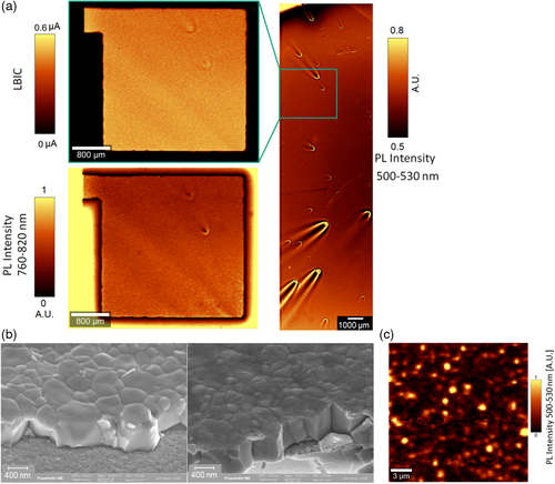
To image the homogeneity of the 2D passivation layer, its emission property as a wide-bandgap semiconductor can be exploited (Figure S4a, Supporting Information). The signal intensity increases with increasing concentration of the applied PEAI solution (compare Figure S4, Supporting Information). By scanning the focused laser excitation over the sample and measuring a spectrum at each scanning position, the homogeneity of the passivation layer can be imaged qualitatively. This is shown on the right side of Figure 3a, with the PL spectra being summed over the wavelength region of interest, that is, from 500 to 530 nm. On this scale, the coverage of the 2D passivation layer is rather homogeneous, with comet-like inhomogeneities induced by small particles in the spin-coated film. After imaging the 2D perovskite, the solar cells are completed with a PCBM and BCP ETL and an evaporated metal electrode. LBIC and spatially resolved PL measurements of the bulk perovskite (spectrum around 800 nm) allow to compare the previously observed inhomogeneities to the charge extraction behavior of the finished solar cells. The thicker 2D regions in front of the two comet-like features yield a lower LBIC signal with simultaneously higher PL signal, emphasizing that charge extraction is hindered there. Nevertheless, the macroscopic coverage of the 2D passivation layer is rather homogenous and the LBIC signal is lower on the full area compared to the non-passivated device (see Figure S11, Supporting Information). SEM images (Figure 3b and S3b, Supporting Information, for a larger scale) also show a very homogeneous coverage of the passivation layer. Interestingly, additional high-resolution PL imaging, depicted in Figure 3c, does indeed reveal inhomogeneities of the PEAI passivation, namely on the micrometer scale. It hence seems plausible that there are regions where an efficient extraction of electrons to the ETL (PCBM) is possible and others where not possible. The charge extraction could for example occur by tunneling of electrons, which depends sensitively on the thickness of the 2D perovskite passivation layer. Note that such small domain sizes of thicker 2D perovskite regions where charge extraction is impeded could not be resolved in the LBIC measurement shown earlier.
Yet alone the inhomogeneity and unfavorable energy alignment for electron transport of the PEAI-based interlayer cannot be the sole origin of the JSC loss, as it shows a particular time dependence. As it will be shown further later, incorporating mobile ionic species into our model can reproduce the experimental findings accurately.
3.5 Ionic Contribution
As investigated by Thiesbrummel et al. ionic space charges can lead to a short-circuit current loss in perovskite solar cells.[27] Similar to the trapped charge-carrier hypothesis, an ionic space charge would lead to a decrease of electron conductivity toward the electron contact and result in charge-carrier accumulation and hence increased recombination in the perovskite bulk, under short-circuit conditions. In the context of the PEAI-passivated devices, the ionic contribution seems rather unintuitive at first glance as the bulk perovskite and hence the density of mobile ions supposedly does not change. To rid the experimental JV-curves from ionic motion during the scanning time, measurements with quasi-constant ion distribution are performed. Before measuring a pair of current and voltage values, the solar cell is kept at either open- or short-circuit for 10 s. The experimental curves obtained in this way are depicted in Figure 4a. It is worth noting that with increasing PEAI concentration, the JSC hysteresis increases. The JSC hysteresis can be read as the difference in JSC between the 0 V ion position scan (solid symbols) and the VOC ion position scan (open symbols).
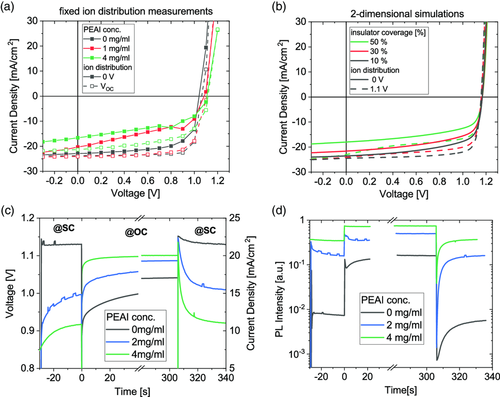
To further evaluate whether there is an ionic contribution, we carried out numerical simulations where a certain fraction of the absorber was either covered by an insulator (thus mimicking the thick PEAI domains) or by the “normal” ETL (thus mimicking those domains where the PEAI was thin enough to allow for efficient charge extraction). The used parameters are given in Table S1, Supporting Information. For the simulations of the JV-curves, the ionic species are first relaxed into their equilibrium distribution during a preconditioning phase with either 0 or 1.1 V forward bias, respectively (in the dark). Then, they are kept in this position during the simulated voltage sweep. These 2D drift–diffusion simulations with incorporated mobile ionic species show that the magnitude of the JSC loss depends indeed strongly on the coverage of the 2D passivation layer. This is revealed in Figure 4b where the simulated JV-curves for varying coverage with thick PEAI are shown. A strong JSC loss is reproduced with increasing insulator coverage from 10% to 50% at the ion distribution of 0 V. In contrast to the simulated devices without mobile ions (Figure S10, Supporting Information), the substantial JSC reduction is already observed at a much smaller device length of 4 μm, which is comparable to the inhomogeneities imaged in Figure 3c. With the ion distribution of 1.1 V, the JSC remains higher, well in accordance with the experimental results.
Next, we investigate the time dependence of the JSC loss as this would constitute another experimental hint for an ionic contribution to the observed phenomena. Figure 4c shows time-dependent measurements of JSC and VOC and Figure 4d shows the simultaneously measured PL intensity. When the light is switched on at t = −30 s, the cell is under short-circuit conditions. In this phase, the PL intensity decreases for all samples, which indicates that charge extraction is enhanced. At t = 0 s, the working point is switched to open circuit. VOC first increases and then saturates during the measured 300 s while the PL intensity stays rather constant. This effect had been described previously.[36] When the cell is switched from open circuit back to short circuit, the measured JSC and the charge extraction is first high and then decreases toward a steady-state value within 20 s. Note that a potential capacitive discharging effect can be ruled out as it would be expected to i) occur in the millisecond timescale and ii) be accompanied by a decreasing PL signal. The observed behavior suggests that there is an ionic contribution to the JSC loss. It becomes clear that already the cell without PEAI passivation is limited by charge extraction losses to some extent, but for the passivated devices, the magnitude of these losses is larger.
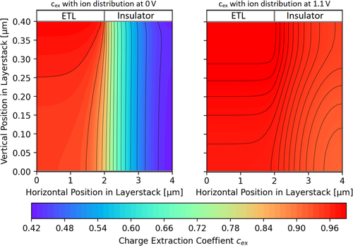
The previously discussed microscopic inhomogeneity of the PEAI passivation layer and influence of the ionic space charge proposes the following mechanism for the JSC loss: under short-circuit conditions, the ions are distributed in a way that the conductivity for the electrons is rather small in the vicinity of the ETL as was shown already in our previous work.[36, 38] As a consequence, many of them cannot reach those domains in the perovskite/PEAI interface within their lifetime where efficient electron extraction is possible. In contrast, with the ion distribution corresponding to open-circuit conditions, the electron conductivity increases and hence (much) more electrons can be extracted. This is illustrated in Figure 5 where the simulated, spatially resolved charge extraction coefficients for the two ion distributions at 0 and 1.1 V, respectively, are depicted. At 0 V ion distribution, the charge extraction from the area covered with an insulator is strongly reduced, whereas at 1.1 V ion distribution, the charge extraction is rather high throughout the whole device. How strong this effect finally is depends sensitively on the fraction and the domain size of the perovskite absorber covered with a (too) thick PEAI layer, and thus on the PEAI concentration (compare simulated, spatially resolved charge extraction coefficients at 0 V ion position with varying insulator coverage, depicted in Figure S12, Supporting Information).
3.6 Mitigation of JSC Loss
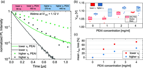
As the proposed mechanism for the JSC loss is the increased recombination in the bulk due to conductivity limitation of one charge-carrier type, the influence of the charge-carrier lifetime on the JSC loss is analyzed. A batch-to-batch variation of perovskite film quality is observable in a nonautomated lab process, possibly due to unintended differences in processing conditions, small stoichiometry variations of the perovskite precursor or operator mistakes. In this paragraph, a worse performing batch (lower power conversion efficiency η) is compared to a better performing batch (higher η). Transient PL measurements of non-passivated (black) and PEAI-passivated (green) perovskite samples on glass, from these two batches, are depicted in Figure 6a. As the analysis of transient PL with single lifetime representation is in some cases misleading, we used the implied VOC (iVOC)-dependent representation proposed by Krückemeier et al.[44]. The iVOC-dependent lifetime data and the formula for the calculation are given in the (Figure S13, Supporting Information). The high-performance batch shows lifetimes corresponding to an iVOC of 1.12 V of τ = 210 ns for the non-passivated and τ = 440 ns for the passivated sample. The low-performance batch yields lifetimes of less than 50% thereof. As expected, and shown in Figure 6b, comparably longer charge-carrier lifetimes of the passivated samples are reflected in higher VOC compared to the non-passivated devices and the longer lifetime batch shows a higher overall VOC. In Figure 6c, it can be seen how strong the impact of the charge-carrier lifetime on the PEAI-induced JSC loss is. This behavior is in line with the mechanism of the JSC loss proposed earlier. In the samples with higher lifetimes, charge carriers accumulating in the bulk due to conductivity limitations have more time to reach the interfaces and can thus contribute to the short-circuit current. This highlights the importance of the perovskite bulk quality, as by reducing non-radiative losses, the impact of the conductivity limitations due to ionic space charge and passivation layers can be minimized.
4 Conclusion
Perovskite solar cells in p–i–n architecture passivated with a PEAI-based 2D perovskite show a strong short-circuit current loss with a simultaneous increase in VOC but a rather constant FF. By combining different experimental methods with drift–diffusion simulations, this study evaluates different possible origins of this short-circuit current loss. By comparing EQE to reflection measurements, it could be excluded that the current loss is due to a change in optical properties. Numerical simulations revealed that a simple low mobility or a band offset of the CTL cannot explain the experimental behavior. The charge extraction coefficient calculated from the PL emission of solar cells in open- and short-circuit conditions revealed that the short-circuit current loss originates in an increased bulk recombination and hence decreased charge extraction. Such an increase of bulk recombination could be caused by (strong) doping of the perovskite bulk or space charges from filled traps and/or accumulated ionic species. CELIV measurements revealed no differences between samples with and without PEAI and further showed in all cases no sign of any bulk doping. Comparing the solar cell behavior in intensity-dependent and transient photocurrent measurements to the simulated behavior renders the hypotheses of a trap-induced space charge extremely unlikely and suggests a strong contribution of ionic motion to the observed current loss. A negative ionic space charge in front of the electron contact would reduce the electron conductivity in this region and thus electrons would be retained from reaching the back contact. This would lead to an accumulation of charge carriers in the bulk increasing the recombination already under short-circuit conditions.
With micrometer-resolved PL spectroscopy, the homogeneity of the PEAI-induced 2D perovskite passivation layer could be imaged and was compared to LBIC measurements of full devices. The inhomogeneous coverage of this layer on the macroscopic scale could be excluded as dominating origin of the short-circuit current loss. However, the detected micrometer-scale inhomogeneity was, by means of numerical simulations, found to play a crucial role in the JSC reduction. The PEAI-based interlayer effectively increases the distance electrons have to travel to be extracted at the interface. In addition, their diffusion length is reduced by the ion distribution under short-circuit conditions. These two effects lead to the observed JSC reduction. An increased charge-carrier lifetime due to enhanced perovskite bulk properties could be identified as crucial, not only for achieving a high VOC, but also for mitigating short-circuit current loss in perovskite solar cells.
5 Experimental Section
Device Fabrication
Solar cells were fabricated on pre-patterned ITO glass substrates (2.5 × 2.5 cm2) with the architecture depicted in Figure S1, Supporting Information. The cleaned ITO glass is treated with 20 min of UV-ozone before applying the hole transport layer.
Hole Transport Layers
The [2-(3,6-Dimethoxy-9H-carbazol-9-yl)ethyl]phosphonic acid (MeO-2PACz, TCI) was dissolved in ethanol (1 mmol L−1) and spun onto the substrate at 4000 rpm leading to a layer thickness too thin to measure with our profilometer and not distinguishable in SEM cross-section measurements. The layer was then annealed at 100 °C for 10 min. Processing of the hole transport layer (HTL) takes place in N2 atmosphere.
Perovskite Layer
The 1.3 m perovskite precursor solution was prepared by weighing PbI2 (TCI) CsI (Sigma Aldrich), methylammonium bromide (MABr), and formamidinium iodide (FAI) (Greatcell Materials) to a stoichiometry of Cs0.05MA0.10FA0.85Pb(I0.95Br0.05)3, adding 5% lead excess with respect to the monovalent cations. The salts were dissolved at 70 °C in a mixture of dimethylformamide (DMF) and dimethyl sulfoxide (DMSO) with the volume ratio 4:1. BMIMBF4 of 0.1 mol% was added directly to precursor solution.
The perovskite layer was deposited by spin-coating the precursor solution at 1000 rpm for 10 s and 5000 rpm for 20 s, dropping the antisolvent ethyl acetate 5 s before the end of the spin-coating process. The film formation was finished by directly placing the sample onto a 100 °C hotplate and annealing for 60 min.
PEAI Passivation Layer
After a short cooling time, phenethylammonium iodide (1–4 mg mL−1 dissolved in isopropanol) was spin-coated dynamically onto the perovskite layer.
Electron Transport Layers
An ETL was applied using a 10 mg mL−1 solution of PC60BM in CHCl3, which was dynamically spin-coated at 4000 rpm. BCP (0.5 mg mL−1 in isopropanol) was dynamically spin-coated as second ETL at 4000 rpm. All these steps were performed in a N2-filled glove box. The cells were completed by thermal evaporation of a 100 nm aluminum back electrode, defining the cell area of 0.0925 cm2.
JV-Curves
JV-scans were performed on a Newport AAA solar simulator corrected for spectral mismatch. The scan speed of the shown JV-curves was 30 mV s−1.
EQE Measurements
A xenon lamp was coupled into a monochromator. The light was modulated with a chopper wheel. The modulated light was focused onto the solar cell, which was illuminated on its full area. The short circuit current signal was measured with a lock-in amplifier.
Transient PL
Transient PL measurements were performed with a UV–vis photomultiplier tube from and a single photon-counting device (Timeharp). The light source was a 515 nm laser (Omicron) that could be modulated digitally with a trigger signal generated by an arbitrary waveform generator. It illuminated a large circular area of around 1 cm diameter. The laser could emit sharp pulses of arbitrary length and repetition rate. The laser power during on-time was adjusted such that in constant-wave mode the JSC of a perovskite solar cell was similar to JSC measured under simulated AM1.5g light.
Micrometer-Resolved PL Spectroscopy and LBIC
A commercially available confocal Raman scanning microscope (Witec) was used to focus a laser beam (355 nm for the 2D perovskite measurements, 635 nm for combined LBIC and PL measurements) onto a sample that is scanned pixel by pixel. The laser spot size was approximately 5 μm for the used objective lens with 10× magnification (images with scale bar 800 and 1000 μm) and 500 nm for the objective lens with 100× magnification (close-up image with scale bar 3 μm). The emitted PL signal was spectrally resolved by coupling it via a dichroic mirror to a Czerny–Turner-type spectrometer and detecting the signal with a silicon charge-coupled device (CCD) linear array detector. For LBIC measurements, the same setup was used for scanning. With a low noise current amplifier, the current output of the cell could be measured at each scanning position.
PL Spectroscopy with Simultaneous JSC or VOC Measurement
Spectral PL measurements were performed with an Andor Shamrock 193i Czerny–Turner-type spectrometer. For graphs that show PL intensity, the recorded spectra were integrated over the wavelength. The illumination source for PL measurements was a frequency-doubled continuous wave (cw) neodymium-doped yttrium aluminum garnet (Nd-YAG) laser from Pegasus laser systems (Pluto, P532.400, 532 nm). Transient voltage or current measurements were performed with a LabVIEW-controlled Keithley 2400 sourcemeter.
CELIV Measurements
The solar cell was reversed biased with a linear increasing voltage ramp produced by an arbitrary waveform generator (Agilent 33220 A, ramp 10 μs, 0 to −0.4 V). The voltage drop over a 55 Ohm resistor was measured with an oscilloscope (Tektronix TDS 2014). For photo-CELIV measurements, the solar cell was illuminated with a 1 μs pulse from a green light-emitting diode (LED).
Intensity-Dependent JSC Measurements
With the same LED, operated in cw mode, the current output was measured with a Keithley 2400 sourcemeter. The illumination intensity was decreased by neutral density filters of known transmission.
Absorption Measurements
Reflection (R) measurements were performed on a Perkin Elmer Lambda 40 UV–vis Spectrometer with an integrating sphere. The Absorption was calculated as 1-R as the samples were solar cells with opaque full area metallization.
Photoelectron Spectroscopy
The samples were prepared and packed under nitrogen atmosphere and transported from Freiburg to Darmstadt. They were opened in a glove box and transferred to the ultrahigh vacuum system. UPS measurements were performed with a Thermo Fisher VG Escalab 250 spectrometer, and the He I (21.2 eV) discharge was used. The pressure inside the analytic chamber was monitored at 2.5 × 10⁻⁸ mbar. A comparison between the initial spectra and later spectra was made to exclude degradation of the samples during the measurement. More details could be found elsewhere.[21]
X-Ray Diffraction Measurements
X-ray diffraction patterns were recorded at room temperature with an XPERT-3 MRD system using a Xe point detector, Bragg–Brentano beam optics, and a Cu–Kα radiation source. Diffraction spectra were recorded between 2θ = 5° and 2θ = 65° at a scan rate of 3.6° min−1 with a step size of 0.03°.
Numerical Simulations
Drift–diffusion simulations were performed using the semiconductor simulation tool Sentaurus Device.[45] The used parameters is found in Table S1, Supporting Information.
Acknowledgements
J. H., C. B., M. U., N. G., J. G., G. L., M. K., U. W. acknowledge funding from the European Union's Horizon 2020 research and innovation programme under the project APOLO (H2020-LCE-2017-RES-RIA), grant agreement No. 763989. C.B., C.M., T.M., and U.W. acknowledge the support from the Deutsche Forschungsgemeinschaft (DFG, German Research Foundation) within the priority program 2196 under project number 423746744.
Open Access funding enabled and organized by Projekt DEAL.
Conflict of Interest
The authors declare no conflict of interest.
Open Research
Data Availability Statement
The data that support the findings of this study are available from the corresponding author upon reasonable request.


