Chemical Solution Deposition of Single-Phase BiFeO3 Thin Films on Transparent Substrates
Abstract
The production of high-quality BiFeO3 thin films on cost-effective transparent electrodes for visible light harvesting applications and devices remains a challenge. Here, the production of single-phase nanostructured BiFeO3 thin films via chemical solution deposition (CSD) on transparent conductive fluorine-doped tin oxide FTO glass substrates is reported. It is shown that BiFeO3 is of high purity using a variety of analytical tools and that the as-obtained BiFeO3 thin films have a single-grain single-domain structure exhibiting ferroelectric switching under poling. The BiFeO3 samples show visible light absorption with a bandgap of 2.7 eV under all processing conditions. By changing the annealing atmosphere, it was possible to modify the photocurrent produced, which were (at 1.23 VNHE) 0.07 (O2-annealed), 0.02 (air-annealed), and 0.01 mA cm−2 (Ar-annealed). This indicates a change in the mobile carriers available. The results show that it is possible to produce single-phase BiFeO3 on a transparent conductive electrode system with controllable photoconductivity.
1 Introduction
Bismuth ferrite (BiFeO3) is a ferroelectric material that has attracted much interest. Its multiferroic behavior with a ferroelectric Curie point Tc = 1030 K and magnetic Neel temperature TN = 670 K lead to a range of unusual and interesting properties.[1] BiFeO3 is also known to be photoactive with a direct bandgap of around 2.7 eV and an indirect bandgap of around 2.2 eV. Both these bandgaps are in the visible region of the solar spectrum. Between 2009 and 2012, it was found that BiFeO3 thin films exhibit switchable ferroelectric diode behavior with a visible light driven photovoltaic effect. This opens up opportunities for multifunctional devices that harvest or collect solar light and perform an energy conversion.[2] The synthesis of BiFeO3 thin films is generally achieved using pulsed laser deposition (PLD),[3] radio-frequency sputtering,[4] molecular beam epitaxy[5], and metal–organic chemical vapor deposition.[6] These methods have successfully produced BiFeO3 films with low leakage current and low defect densities. They are not promising choices for large-scale BiFeO3 thin-film processing due to the expensive facilities needed and, in the case of chemical vapor deposition reported to date, complicated substrates preparation procedure. A low-cost route for preparing high-quality BiFeO3 thin films with robust ferroelectric properties is a key and vital next step for many practical applications.
Chemical solution deposition (CSD) is a common method for fabricating functional thin films that can have controlled thicknesses in the nm range or tailored surface morphology.[7] It has the advantages of easy fabrication and is scalable for large area film synthesis. It is well known that BiFeO3 can easily form parasitic phases and defects for a variety of reasons being suggested.[8] BiFeO3 has been reported as being metastable, off-stoichiometric, and easy to lose Bi during annealing. This leads to secondary phases or a highly conductive film with high leakage.8, 9 The control of BiFeO3 phase becomes more challenging when using CSD since the precipitation of impurity phases can happen during the heating cycle of film synthesis. Impurity phases compromise the functional performance of BiFeO3. For example, BiFeO3 films with Fe2O3 show a ferromagnetic behavior rather than the low bulk-like magnetic moment exhibited by single-phase BiFeO3 films. The growth of conductive Bi2O3 creates an electric short circuit through the BiFeO3 film.8 Dedicated control of the film gelation process to obtain a homogeneous gel film before annealing has been suggested to be critical for CSD-synthesized epitaxial BiFeO3 film.[10] One general recipe used is to use a slightly higher Bi:Fe ratio than 1:1 producing a Bi-excess in the films. This compensates for Bi losses during annealing and suppresses the formation of Bi and O vacancies.[11] O2 has been used as the annealing atmosphere to compensate for oxygen vacancy formation.[12] However, these additional processing steps bring problems such as the formation of bismuth-rich phases or an increase in the cost and complexity of the fabrication of the thin films.
In applications such as solar active devices and photochemical cells, the system often requires transparent electrodes to enable light to activate the film via the back interface.[13] In these instances, the BiFeO3 thin film needs to be produced on industry-standard transparent substrates such as fluorine doped tin oxide (FTO) or indium doped tin oxide (ITO) coated glass. Deposition of a BiFeO3 thin film on readily available, transparent and conductive FTO glass is a preferable choice for a wide range of applications.
Here we demonstrate that we produce high-quality BiFeO3 film which is a single phase. The photoelectrochemical properties of the BiFeO3 thin films annealed under oxygen, air, and argon were studied and are shown to be compatible with previous studies for BiFeO3 films. The ferroelectric property of the BiFeO3 thin film was characterized using piezoresponse force microscopy (PFM) and switchable polarization was demonstrated. This is indicative of the as-prepared BiFeO3 films having good ferroelectric properties. The results provide a CSD approach to prepare polycrystalline BiFeO3 thin films. This paves the way to use the material in photovoltaic, photochemical, and ferroelectric devices.
2 Results and Discussion
We have used acetic anhydride as the dehydration agent and carefully controlled the substrate temperature during gelation. Through this process, we have successfully produced a BiFeO3 thin film on FTO-coated glass that has properties consistent with a previous report on single-crystal substrates.[10] A photo of the BiFeO3 film (Figure S1, Supporting Information) demonstrates its good transparency. A review of the X-ray diffraction (XRD) patterns (Figure 1) shows that a polycrystalline single-phase BiFeO3 film has been produced after annealing in oxygen, air, and argon. It is not necessary to have an oxygen-rich atmosphere to produce high purity BiFeO3 thin films.
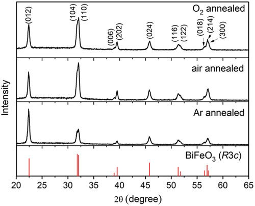
Looking at the XRD patterns, Figure 1, of the as-annealed BiFeO3 thin films in more detail we find all the films show well-crystallized rhombohedral structures. This match and the absence of secondary-phase peaks demonstrate the high purity of the samples. Close investigation of the (012) peak for the three annealing regimes shows some differences. In the case of the Ar-annealed sample, there is a higher intensity of the (012) peak compared to the (104)/(110) peaks. For the O2- and air- annealed BiFeO3, the (012) has a lower relative intensity to (104)/(110), which suggests that different annealing atmospheres can lead to different orientation for grain growth. A similar effect of different annealing atmospheres on the orientation of grain growth was also reported in the work by Thundat et al.[14] The refinement of crystal structures was carried out by means of the GSAS software suite,[15] to evaluate the effect of the annealing atmosphere on the crystal structure of BiFeO3. A rhombohedral model (α = 5.58197(3) and c = 13.87773(9) Å in the space group R3c) was applied in structure refinements.[16] The refinement results are shown in Figure S2, Supporting Information, to allow the comparison of ferroelectric distortion for BiFeO3 annealed at different atmospheres, all the lattice parameters were converted to the pseudocubic equivalent cell with aPC = aR/ and cPC = cR/2 and VPC = VR/6. The crystal structure distortion (cPC/aPC) of O2−, air−, and Ar− annealed BiFeO3 are 1.0148, 1.0148, and 1.0151 (details shown in Table S1, Supporting Information), respectively. The distortion values are very close, indicating that annealing in the three different atmospheres did not change the long-range crystallographic structure of the BiFeO3 thin films.
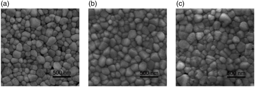
Figure 2 shows scanning electron microscope (SEM) images of the BiFeO3 thin films annealed. The SEM images on a microscopic scale can be found in Figure S3, Supporting Information. The BiFeO3 films exhibit a polycrystalline and compact morphology with the grain size ranging from around 50 to 300 nm for samples produced under all annealing atmospheres. This observation differs from previous reports that O2 atmosphere is essential for the preparation of BiFeO3 thin films with high-quality crystallization. It is rare to see a compact morphology due to the difficulty in BiFeO3 synthesis although under our process we have achieved a high-quality film. Achieving a dense morphology is important for applications of BiFeO3 thin films especially when nanostructured or produced with nm level cross-section. It is necessary to produce a film without holes or voids to minimize electrical short circuits in the device.[17]
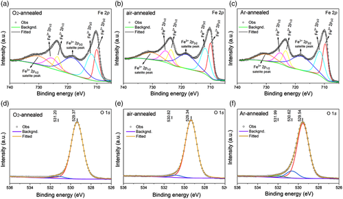
To investigate the effect of the annealing atmosphere on the oxidation state of Fe and O, X-ray photoelectron spectroscopy (XPS) was performed on the as-prepared BiFeO3 thin films. The fitted Fe 2p and O1s spectra for the three samples are shown in Figure 3. The fitting data of Fe 2p and O 1s are summarized in Table S2 and S3, Supporting Information. The characteristic 2p3/2 and 2p1/2 peaks of Fe were separated by 13.6 eV.[18] The Fe 2p1/2 (≈730 eV) and Fe 2p3/2 (≈718 eV) satellites peaks occur at the high-binding-energy side of each main peak. Two peaks located at ≈712 eV (characteristic peak of Fe3+) and ≈710 eV (characteristic peak of Fe2+) are obtained after fitting of Fe 2p3/2 peaks of three samples, indicating that Fe2+ exists in all three samples. A review of Table S2, Supporting Information shows that the valence of Fe relates to the film annealing atmosphere, and more Fe2+ formed under oxygen-deficient condition, which is consistent with previous studies.[19] The production of more Fe2+ can be related to a higher defect density in the sample. The O1 s peak can be resolved into two subpeaks located around 529 and 531 eV, corresponding to the lattice oxygen and oxygen associated with oxygen vacancies.[20] The Ar-annealed sample shows an additional peak at ≈532 eV, which can be attributed to oxygen bonded to carbon.[21] Comparing the peak area in Table S2, Supporting Information, it can be seen that annealing in an oxygen-deficient atmosphere resulted in more oxygen vacancies. Analysis of the Fe 2p and O 1s XPS spectra indicates that annealing in oxygen-deficient atmosphere results in more Fe2+ with consequent formation of oxygen vacancies.
The domain structure and switching properties of the BiFeO3 thin films were characterized by piezoelectric force microscopy (PFM), shown in Figures 4 and S4, Supporting Information. Phase image shows bright and dark contrast corresponding to the domain orientation toward and opposite to the applied field direction. It can be seen from the topography and phase (domain) images that the BiFeO3 thin films have a single domain structure within one grain. This suggests that the grain size is too small to produce domain walls within a grain.[22] This unique single-domain-single-grain polycrystalline structure can be used for a mechanistic study of polycrystalline BiFeO3 film in multifunctional applications without a domain wall contribution.[23]
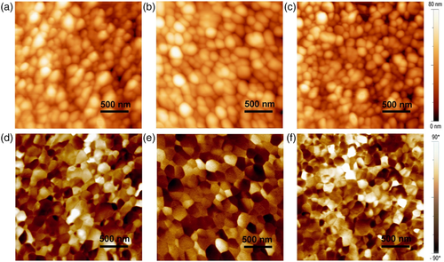
Figure 5a shows the UV–vis spectra of the three thin films with Figure 5b showing the derived Tauc-plots. From the absorption spectra, it can be seen that the BiFeO3 thin films annealed in different atmospheres have a very close light absorption onset and show a good visible light absorption. Tauc plots in Figure 5b show that the three samples have a consistent bandgap value of around 2.7 eV. This characterization indicates that the annealing atmosphere does not make significant differences to the bandgap of the thin films. It should be noted that the bandgap of BiFeO3 has many reported values ranging from 2.1 to 2.8 eV, owning to its complex defect nature. Typically, the loss of Bi and O during annealing or the valence change of Fe leads to a change in the bandgap.1, 24 The atmosphere used during annealing has been shown to affect the defect structure of BiFeO3 by influencing Bi and O loss. The results here suggest that by controlling those conditions with a short annealing duration of 1 h and a low annealing temperature of 650 °C, it is possible to remove the influence of the atmosphere on bandgap.
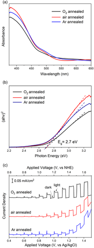
The photochemical properties of the BiFeO3 thin films were characterized in a photoelectrochemical (PEC) cell. Figure 5c shows the photocurrent–voltage (J–V) curves of BiFeO3 thin films illuminated under chopped AM1.5G illumination. The photocurrents at 1.23 VNHE were 0.07 (O2-annealed), 0.02 (air-annealed), and 0.01 mA cm−2 (Ar-annealed). These are comparable to previously reported BiFeO3 films prepared by PLD (0.06 mA cm−2 at 1.1 VNHE under 1 sun)[25], sputtering (0.01 mA cm−2 at 1 VNHE under 1 sun)[26] and hydrothermal (5.2 μA cm−2 at 1.0 V vs. saturated calomel electrode, 500 W Hg lamp) method.[27] The good performance can be attributed to the compact morphology and well-crystallized structure. The J–V results demonstrate that BiFeO3 thin films prepared by the CSD method are promising candidates for photochemical applications.
The photocurrents show a decreasing trend with the annealing atmosphere changing from O2 to air and Ar. When the applied voltage reached 1.4 VNHE, the dark currents of all samples increased. This was most notable in the Ar-annealed sample. This is indicative of highly mobile carrier flow through the film. We relate this to the increased Fe2+ content in the films annealed under the oxygen-deficient condition as indicated in the XPS results. Electrons in the BiFeO3 film can hop between Fe2+ and Fe3+ sites and result in a conducting behavior.[28] This acts to compromise the photochemical performance and ferroelectric properties of the film. The BiFeO3 films here were prepared by repeating the precursor solution deposition procedure five times and the obtained thickness was around 150 nm, observed under SEM. The choice of five layers was optimized from our earlier experimental work. A thinner BiFeO3 film prepared by depositing less than five layers showed large dark/leakage currents due to bad film coverage on the FTO surface while a thicker film showed limited photocurrents due to the weak hole transport ability under back-side illumination. It was demonstrated by Pala et al. that the back-side illuminated photocurrents decay exponentially with respect to the film thickness.[29] This is attributed to the short hole diffusion length of the material (typically a few nanometers).[30]
It is worth noting that current spikes are observed in all three samples under low applied bias. These include positive spikes when switching from dark to light and negative spikes from light to dark. These spikes have been attributed to the surface recombination of photoexcited carriers.[31] The positive spikes were resulted from the accumulation of holes at the electrode/electrolyte interface, which injected to the electrolyte once light on. While the latter decreased but steady photocurrents were generated by holes diffused to the interface, which have a kinetic limitation. The negative spikes, likewise, were generated by the back reaction of electrons from the conduction band with the accumulated holes. At higher potentials, the spikes disappeared since the carries obtained enough driving force and the holes that reached the surface can inject into the electrolyte more freely. This behavior is in turn related to the surface traps or defects.[32] In general, the current spike scale of the O2-annealed sample is smaller than the air-annealed sample. The largest current spike is for the Ar-annealed sample. This adds more evidence to the XPS data to indicate that higher O2 annealing leads to a reduced number of traps and defect densities. Thus, while the atmosphere of anneal does not change the phase pure nature of the BiFeO3 a higher O2 annealing atmosphere is preferable for BiFeO3 photoelectrode processing.
3 Conclusion
BiFeO3 thin films on FTO glass substrates were successfully fabricated via a CSD method. We show that pure phase BiFeO3 thin film can be produced in either oxygen-rich or deficient annealing atmospheres. The BiFeO3 thin films show a direct bandgap value of 2.7 eV irrespective of the annealing atmosphere. The BiFeO3 thin films show a single domain polycrystalline structure due to the small grain size. PFM characterization of the BiFeO3 thin films demonstrated they have a ferroelectric nature. The BiFeO3 thin films exhibit good photochemical performance. There was a noticeable relationship between the annealing atmosphere and measured photocurrent due to the variations in defect density associated with annealing. Our results demonstrate that it is possible to fabricate high-quality BiFeO3 thin films via a simple CSD method. We demonstrate a promising technique for large-area BiFeO3 thin films in the memory device, photochemistry, and photovoltaic areas.
Acknowledgements
The authors would like to acknowledge the Chinese Scholarship Council for supporting this work. Financial support from LSBU are acknowledged.
Conflict of Interest
The authors declare no conflict of interest.
Open Research
Data Availability Statement
The data that support the findings of this study are available from the corresponding author upon reasonable request.


