High Vapor Transport Deposition: A Novel Process to Develop Cu2ZnSn(SxSe1–x)4 Thin Film Solar Cells
Abstract
Kesterite thin film solar cells are known to be a promising cost-effective solution because they are based on earth-abundant and environmental compounds. However, it is known that their best efficiency (12.6%) has not been improved since 2013, meanwhile other thin-film solar cells have demonstrated that their performance has been enhanced continuously. The main drawbacks to explain this situation is the narrow process window of this compound and simultaneously, the high composition and thermal control needed to avoid intrinsic defects in the p-type layer. The high vapor transport deposition process has not been explored yet by kesterite thin film solar cell developers. Herein, we present the results obtained using a design of a new vacuum deposition method similar to close space sublimation, which reported excellent results in CdTe. The main advantages of this novel process are: 1) to achieve a high deposition rate; 2) to be able to deposit precursor materials and to carry out the sulfur-selenization in the same process chamber, avoiding the two steps used in the sequential process; 3) to provide a high accuracy in the chemical composition control; and 4) simple design using commercial components to facilitate its scalability for large production.
1 Introduction
Materials such as cadmium telluride (CdTe), copper indium gallium selenide (CIGSe), and copper zinc tin selenide (CZTSe) with higher absorption coefficient are trying to make headway in the competitive photovoltaic market covered mainly by silicon materials.[1] The most important key factors of those emerging semiconductors are the cost-effective mass production, together with high photovoltaic conversion factor (PCE) and long-term stability. Despite CdTe and CIGSe are already industrialized, and their PCE is reaching the commercial silicon ones, the kesterite (CZTSe) is still an emerging technology with high absorption and low raw material cost. But one of its main bottlenecks is its hidden capability to be manufactured at large scale with reasonably good quality.[2]
The CZTSe has the properties desired for photovoltaic materials to be selected as potential p-type semiconductors: direct bandgap, high absorption coefficient (104 cm−1 in the visible light range), and optical bandgap energy of the range 1.4–1.5 eV, close to the optimum single-junction value predicted by Shockley–Queisser model. Today, CZTSe is considered a good competitor for CIGS-based solar cells. CZTSe is described by the structural model of two natural minerals: stannite (space group I-42 m) and kesterite (space group I-4).[3-5] These structures are very similar: in both structures the cations are located on tetrahedral sites, but their distributions on planes perpendicular to the x-axis are not the same. Additionally, the position of the chalcogen atom is slightly different in both structures. Design and manufacturing of high efficiency CZTSe solar cells need high accuracy in the composition of the absorber material: slight modifications in composition, structural electronic, and defect properties of the alloys have a high impact in the bandgap energy.[6]
CZTSe solar cells have achieved the highest efficiency of 12.6%,[7] which is still far from the offered by CIGS-based solar cells: 23.35%.[8] It has known that this limitation is mainly related with the short minority carrier lifetime and the high series resistance imposed by the contact barrier due to the formation of the MoSe2 at the CZTSe/Mo interface. The presence of secondary phases and defect states in the absorber also increases the recombination rate.[9, 10] The influence of the deposition method on the structure, morphology, optical, and electrical properties of CZTSe has been investigated by other researchers: sputtering, thermal evaporation, spray pyrolysis, electrodeposition, dip coating, SILAR method, spin coating, sol–gel, solvothermal method, and chemical bath deposition (CBD).[1] In all of these techniques, the control of the presence of secondary phases is the major critical issue, so the final performance of the device is dependent on the manufacturing route selected: the highest conversion efficiency of CZTS achieved using vacuum techniques such as sputtering, thermal evaporation, etc. was over 10%,[10, 11] whereas the highest achieved efficiency of CZTS thin film solar cell by nonvacuum techniques such as spray pyrolysis, sol–gel, etc. was about 12.6%[7] as reported by Wang et al. Nowadays, it is needed to understand the connection between the deposition method of the semiconductor and its intrinsic properties, to guarantee mass production, which is very limited compared to other types of photovoltaic devices such as CIGS and CdTe.
Vacuum deposition methods are those most often selected to fabricate thin film photovoltaic modules at large scale. They are very simple, modulable, better use of raw materials, high production rate, and with better quality to ensure reliability to the process. Typically, two approaches are followed: vacuum thermal evaporation and sputtering. Desired composition is controlled by both techniques adjusting the deposition rate of metal targets (sputtering) or metal sources (evaporation). However, both methods have also some drawbacks. Evaporation employs the Cu, Zn, and Sn evaporation sources (evaporation temperature close to 1000 °C) with Knudsen type, and Veeco S/Se source box in metallic tantalum at the annealing temperature of 550–575 °C during 5 min.[12, 13] The sputtering approach needs a two-stage process: first, Cu–Zn–Sn precursors are deposited by DC magnetron sputtering, and second, the deposited materials are submitted to one annealing in the range of 400–500 °C for 40–60 min under N2 atmosphere after deposition, in a separate furnace. Moreover, during the annealing, once the substrate temperature reaches above 400 °C, the Sn loss is high. In both cases, it is observed a lack of thermodynamic stability and losses of Sn and (S,Se) species due to the high substrate temperature applied during the annealing. The consequences are: 1) the formation of secondary phases such as Cu2SnS3, Cu2SnSe3, Cu2Se3, CuSe2, ZnS, and others; 2) relative low control of the desired stoichiometry. In both cases, the result is that the efficiency of the device is reduced.
Another promising vacuum alternative is known as vapor transport deposition (VTD), which is well extended in manufacturing other thin films materials like CIGS, CdTe, or Sb2Se3.[14, 15] This approach, modified from the classical chemical vapor deposition (CVD), is attractive because it offers high deposition rates, source and substrate environment conditions are decoupled, lower evaporation temperature for the raw materials, and it can be easily scaled up for large mass production, as it was demonstrated by First Solar with commercial photovoltaic modules of CdTe. In spite of these advantages, there are few reports of experimental studies to create CZTSe thin films using VTD, and to the best of our knowledge, this approach has not been optimized and reported in the literature in deep detail. Only Sagna et al.[15, 16] reported achievements obtaining thin film of CZTS using VTD route, but they were unable to remove CuI residual phase of the transportation process, and they obtained the CZTS thin film from a previous CZTS ingot raw material created in a vertical furnace at 1080 °C during 8 h for ensure homogeneity. Our HVTD design allows the capability to create the absorber layer from Cu, Zn, Sn, and S/Se powder directly, which has opened a new process window to achieve a gradient composition profile S/(S + Se) in the absorber. Also, the design has been optimized to achieve fast deposition rates compared to conventional evaporation or sputtering methods.
In this study, we present a novel HVTD process which allows the capability to create the absorber layer from Cu, Sn, Zn and S/Se powder in only one stage, using lower temperature than conventional evaporation, and with high control of chemical species. These operational conditions open a new process window to enhance quality properties of CZTS and to achieve gradient composition profiles (S/Se). Also, the configuration of the equipment has been optimized to ensure high deposition rate compared to evaporation and magnetron sputtering processes.
So, the aim of this work was to develop a HVTD process to demonstrate that CZTS absorber layers can be fabricated with easiest tuneability with respect to conventional vacuum processes: sputtering + annealing or coevaporation, and in only one stage. In this HVTD process, both the substrate temperature and the distance between the source and the substrate are decoupled and adjustable. Also, the source temperature for precursors and the gas flow from them are flexible and independent enough to ensure optimum and fine stoichiometry control in the semiconductor layer: good crystallinity, free of secondary phases, and reduced bulk and interfacial defects. This means lower carrier recombination losses. Additionally, in this research study we have demonstrated that thanks to the fine control of the raw materials composition, it is possible to obtain a gradient profile composition which has positive effects on the bandgap and performance of the solar cell. Finally, the design of the equipment is easy to scale up for large production.
2 Experimental Section
2.1 Preparation of the CZTSSe Thin Films
This research is based on the process HVTD, which is capable to create the CZTSSe semiconductor thin film in one step, with the additional advantage of decoupling the source and substrate temperature. First, a glass substrate with an area of 4 × 4 cm2 was coated with a layer of molybdenum (Mo) with a thickness of 800 nm as the back contact layer. Mo deposition was carried out in a DC sputtering under an argon (Ar) atmosphere with a pressure of 5 × 10⁻³ mbar, in a pilot scale 30 × 30 cm2. Later, this piece of glass was cut in small samples to be loaded in the HVTD process chamber.
HVTD equipment is formed by two chambers (Figure 1): load-lock and process chamber, both of them adapted to high vacuum system (rotary and turbomolecular pumps). A set of stainless steel shields with sheathed microheaters are attached to the process chamber walls. The chamber has a hollow flange fixed on three supports on a bottom plate in the center, for the installation of the sample holder, and inside of this flange there is a heater and piping for temperature control of the substrate. On the top of the process chamber, there is a lid with fixture to fix the shower head and one flange to connect with the gas mixture chamber. Sample table is a SUS 304L hollow inside disc, which is supported on three pins on the chamber bottom. Inside, there is a sheathed microheater made of spiral coil and coolant media pipes, so temperature of the sample can be adjusted from room temperature to 700 °C, thanks to one PID control provided by a thermocouple, with a heating and cooling ramp of 50 °C min−1.
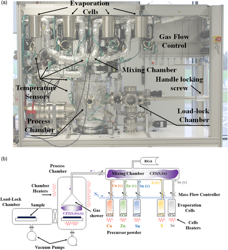
The equipment has also one mixing chamber connected to the evaporation sources. The target of these chambers is to ensure the proper stoichiometry of the raw materials prior to the deposition on the substrate. For that purpose, the evaporation sources are connected to individual pipes where a carrier gas is flowed. The flow of the injected carrier gas is controlled with an automatic mass flow controller. So, the equipment is capable to adjust the desired stoichiometry in a wide range of compositions with high accuracy, thanks to the temperature control of the evaporation source where the precursor is located, and the flow control of the carrier gas to transport it into the mixing chamber. Additionally, the mixing chambers have one port connected to one mass spectrometer (200 amu range) to monitor in real time the composition of the gas mix. This equipment feeds the computer to adjust automatically the temperature and carrier gas flow settings.
Each mixing chamber has a heater made of a micro sheathed heater as a coil, placed on SUS cylindrical reflector inside the chamber. Temperature is controlled by some thermocouples with PID control, and temperature is adjustable in a range from room temperature till 600 °C. Finally, all components used for the assembly of the equipment are available commercially to ensure the technology transfer to large-scale production.
HVTD is built with eight individual evaporation sources, connected to the mixing chamber. Each evaporation source[17] is a cylinder with top flange CF type connected with top lid by a metal gasket. Top lid has two pipes welded: one is used for carrier gas inlet and the second for outlet. Vapor coming from the raw materials will be transported to the mixing chamber using one carrier gas, and to avoid undesired solidification during the transport, each carrier gas can be heated until 500 °C before entrance to the evaporator and the pipes are micro sheathed heated winded around the outer walls.
2.2 Characterization
The composition of the absorbers was measured using X-ray fluorescent (XRF) equipment (Fischerscope XDV-SDD) reporting the average value of five points per sample: the corners and the center of the film. Secondary ion mass spectroscopy (SIMS) technique (ION-TOF model 5) was used to determine the depth profile composition of the p-type absorber films. The equipment was equipped with a Bu primary ion gun and a Xe sputter source, and the energy used for the Xe excitation source was 2 and 30 keV for the Bi+ ions; the aperture area during the scanning was 300 × 300 μm2. SIMS equipment is calibrated to ensure a lateral resolution of 3–10 μm. The phase composition and crystalline structure of the CZTSSe thin films were analyzed by using a X-ray diffraction (XRD) equipment with Cu Kα radiation (1.5416 Å) (Panalytical) in θ–2θ configuration. Phases and order–disorder analysis were determined by using a homemade Raman spectrometer with a laser excitation of 532 nm; the laser beam was focused to ≈1 μm in diameter with a 50× microscope objective. During the characterization, the laser power was kept below 5 mW to avoid any undesired crystallization of the absorber induced by the laser excitation. The optical properties and the bandgap of the kesterite samples were calculated from transmissivity and reflectivity measurements through one monochromator (Newport, model 74 100), UV–vis–NIR photodetectors (Newport, models 71 580 and 71 585), and lock-in amplifier (SR 870 dual phase). The excitation source consisted of one halogen lamp (Newport, model 71 228). The incorporation to the setup of one integrating sphere (BFI Optilas, model RT-060-SF) allowed to determine the influence of the absorber surface roughness on the optical properties. The current–voltage (J–V) characteristics of the solar cells fabricated were measured using a solar simulator class AAA (ABBET Sun 3000 AAA 3 kW) under standard test conditions (STC): solar irradiance 1000 W m−2 AM1.5G and 25 °C cell temperature. Before any J–V measurement was made, the solar simulator was calibrated with a reference solar cell to ensure the optimum equipment setup.
3 Results and Discussion
3.1 Compositional Properties of CZTSSe Thin Films
The chemical composition of the CZTSSe samples was determined by XRF technique, and they are reported in Table 1. The given compositional values were determined by considering average values of five nonalignments points on each sample. Along the experiments, the flow of the precursor materials was modified to obtain pure CZTS, CZTSe, and intermediate phases CZT(S,Se), and the deposition time was optimized to guarantee the same thickness in all absorbers.
| Sample | Chemical composition [%] | Chemical Composition Ratios | ||||||
|---|---|---|---|---|---|---|---|---|
| Cu | Zn | Sn | Se | S | Cu/(Zn+Sn) | Zn/Sn | S/(Se+S) | |
| CZTS | 29.43 | 22.26 | 18.71 | – | 29.60 | 0.72 | 1.19 | 1.00 |
| CZTSSe #1 | 15.28 | 16.32 | 12.47 | 47.02 | 8.91 | 0.53 | 1.31 | 0.16 |
| CZTSSe #2 | 17.16 | 18.27 | 11.09 | 42.47 | 11.01 | 0.58 | 1.65 | 0.21 |
| CZTSSe #3 | 19.30 | 17.10 | 12.24 | 38.12 | 13.24 | 0.66 | 1.40 | 0.26 |
| CZTSSe #4 | 28.87 | 15.13 | 11.32 | 32.67 | 12.01 | 1.09 | 1.34 | 0.27 |
| CZTSSe #5 | 30.36 | 15.84 | 10.67 | 30.21 | 12.92 | 1.15 | 1.48 | 0.30 |
| CZTSe | 28.96 | 26.84 | 16.27 | 27.93 | – | 0.67 | 1.65 | 0.00 |
CZTSSe samples show a progressive increase in the Cu/(Zn+Sn) ratio, from 0.53 to 1.15, due to the incremental content of Cu and a slight loss of Zn in the absorber layer during the sulfo-selenization. This phenomenon has been reported by several groups to be a consequence of elemental sublimation at high temperature.[18-20] Also, all samples are Zn rich. The change in the elemental composition was due to the sulfur incorporation into CZTSe structure. Sample series were designed to achieve Cu-poor and Cu-rich CZTSSe absorber layers. The recommended composition for the fabrication of solar cells with high performance is Cu/(Zn+Sn)<1 (Cu-poor) and Zn/Sn>1 (Zn-rich).[21-23] The nonstoichiometry composition measured may be due to two hypotheses: the coexistence of secondary phases and the high concentration of intrinsic defects.
SIMS is a complementary method for XRF to analyze not only the composition of the films, but also the elemental distribution as a function of depth. Figure 2 shows the compositional profiles of some of the samples manufactured: CZTSe, CZTS, and CZTSSe with different S/(Se + S) ratio. The region where the Mo signal rises fast determined the position of the absorber and back contact interface. The intensity of the S and Se signals decreases toward the back contact region, but there is a slight diffusion of (S,Se) atoms into the Mo layer, which results into a Mo(S,Se)2 interface. These impurity atoms might act as trap centers, and this leads to the reduction of the cell's efficiency.
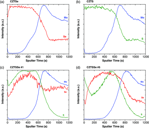
It is observed that sample CZTSSe #5 shows a heterogeneous Se and S distribution across the depth of the absorber layer, which has been previously reported[24, 25] that can be advantageous from the solar cell performance point of view. This result demonstrates the capabilities of the HVTD deposition technique to ensure high control and optimization of the chemical composition, with positive consequences on the finished device. Thus, when the S/(Se + S) ratio is controlled during the absorber formation, the cation substitution tunes the bandgap of CZTSSe absorber films.[26, 27]
Jiang et al.[28] concluded that this gradient of S composition across the CZTSSe bulk resulted in a V-shaped energy gap profile. This design has been reported previously with some limitations, mainly due to the high volatility of S and Se raw materials,[29] but this experimental approach ensures stable conditions to achieve a fine tune of the desired composition of the absorber layer. This phenomenon is similar to that observed in CIGS semiconductors when the Ga content has not a uniform depth profile. As a consequence of the linear decrease of the bandgap of CZTSe compounds with the increase of Se content, several advantages are identified: 1) the bandgap of the absorber p-type layer can be adjusted in the range of 1.5–1.0 eV according to the S/(Se + S) ratio selected; 2) the bandgap grading approach provides an additional electric field which reduces the recombination of the carriers; 3) the band alignment between p- and n-type layers is aligned, minimizing the spike observed with the CdS n-type layer[30]; 4) the open-circuit voltage of the device is increased.
3.2 Structural Properties of CZTSSe Thin Films
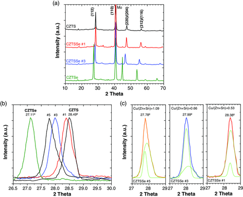
The crystallographic structure and the orientation of the samples have been analyzed by XRD technique, in the range 10–80°. XRD patterns with different sulfo-selenized absorbers are shown in Figure 3, showing a polycrystalline nature. The main reflections at 27.26°, 44.82°, and 53.64° can be assigned to (1 1 2), (2 2 0), and (3 1 2) planes of the CZTSe kesterite structure (JCPDS # 52-868), which is in good agreement with previous data (Gang 2016, Yang 2017). It is observed that Bragg reflections are shifted to higher diffraction angles with respect to pure CZTSe structure, which suggests that these films exhibit a CZTSSe phase. Pure CZTS structure is also observed showing a different (1 1 2) reflection position (28.44°) (JCPDS # 26-0575). A similar variation is observed for (2 2 0) and (3 1 2) reflections. This shift (Figure 3b) is consequence of the sulfur incorporation into the pure CZTSe structure, consistent with previous XRF measurements. Unfortunately, the coincident reflections (2 2 0)/(2 0 4) and (3 1 2)/(1 1 6) remain unresolved. All phases detected in the XRD patterns maintain their reflections at consistent diffraction angles according to the S/(S + Se) ratio. Intermediate CZTSSe films reveal a non-Gaussian profile in the main reflection (Figure 3c). Tailing is observed in the right caused by the sulfur addition in the CZTSe structure. Apparently, the XRD analysis does not show the presence of secondary phases like Zn(S,Se), Sn(S,Se), and Cu2(S,Se), which means that the absorber layer has good quality to be used as p-type layer in the solar cell.
| Sample | S/(Se+S) | D [nm] | ε [×10−2] | δ (×10−4) [nm−2] |
|---|---|---|---|---|
| CZTS | 1 | 48.21 | 7.19 | 4.30 |
| CZTSSe #1 | 0.16 | 41.30 | 8.02 | 5.86 |
| CZTSSe #2 | 0.21 | 42.61 | 8.17 | 5.51 |
| CZTSSe #3 | 0.26 | 43.22 | 8.39 | 5.35 |
| CZTSSe #4 | 0.27 | 42.73 | 8.26 | 5.48 |
| CZTSSe #5 | 0.30 | 42.38 | 8.18 | 5.57 |
| CZTSe | 0 | 47.09 | 7.36 | 4.51 |
To confirm the presence of CZTSSe and potential additional binary phases, the samples were characterized by Raman scattering (Figure 4).
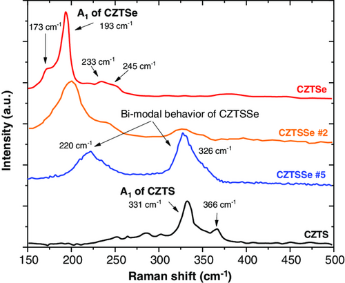
Figure 4 shows the Raman spectra for the fabricated CZTSSe films with different S/(Se + S) ratio. Raman analysis shows broad peak positions located in the range of 331–to 193 cm−1; limits that correspond to the A1 mode peaks for pure CZTS and CZTSe compounds, respectively. A1 mode for CZTSSe films is caused by symmetric vibrations of S and Se atoms surrounded by motionless neighboring atoms.
It is observed that the 170 cm−1 mode vanished when S atoms are incorporated in the absorber film. According to Chen et al.,[34] the Cu atoms diffusion from the surface to the bulk of the film could lead a reduction in the energy formation of VCu acceptor defects minimizing undesired effects from CuZn antisite defects and potential back contact barrier between the absorber and MoSe2 layers.[35] Results presented in Figure 4, more specifically sample CZTSSe #5 (blue line), are consistent with these defects as the sample is Cu-poor. Sample CZTSSe #2 (orange line) showed that the intensity of the 245 cm−1 mode, associated to ZnSe phase in the Zn-rich absorbers, increased with respect to the pure CZTSe sample. This result suggests that the manufacturing condition for this sample leads to an increase in Zn composition with respect to the other films, which is in line with the previous presented results from the XRF analysis. According to Dimitrievska et al,[36] this process condition should reduce detrimental 2CuZn+SnZn defect clusters and the desired formation of VCu and ZnCu point defects, which is expected to increase the performance of the solar cell.
3.3 Solar Cell Performance
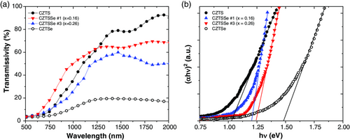
So, to determine the impact of the compositional and structural properties of the CZTSSe in the solar cell performance requires the analysis of the optical properties. Hence, we have carried out spectrophotometric measurements of transmissivity (T) and reflectivity (R) to determine optical parameters, like the absorption coefficient (α) and the bandgap (Eg). Transmissivity measured as a function of the S/(S + Se) ratio is shown in Figure 5a. It is observed how transmissivity in the vis–NIR region is increased with the S content; meanwhile, in such region the pure CZTSe phase exhibits values lower than 20%. Optical properties were measured with and without using an integrating sphere to compare the scattering effects from the surface. With this experimental approach we were unable to determine quantitatively the surface roughness of the samples, but from a qualitative point of view we observed that absorbers with sulfur exhibited a lower surface roughness, which means lower diffuse reflected light compared to the direct reflected component.
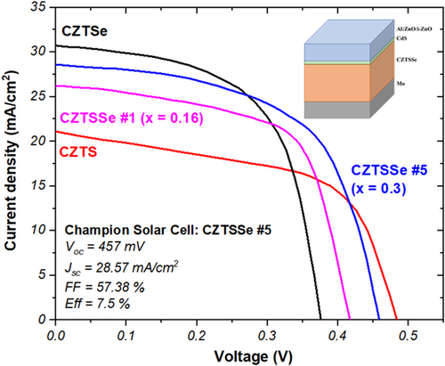
To investigate the device performance under the different manufacturing conditions, solar cells with an Al:ZnO/i-ZnO/CdS/CZTSSe/Mo structure were fabricated, and no additional antireflecting coating was used. J–V curve measured at STC is illustrated in Figure 6, and solar cell performance parameters such as open-circuit voltage (Voc), short-circuit current density (Jsc), fill factor (FF), and efficiency are detailed in Table 3.
| Sample | V oc [mV] | J sc [mA cm−2] | FF [%] | Eff. [%] |
|---|---|---|---|---|
| CZTS | 483 | 21.19 | 54.74 | 5.6 |
| CZTSSe #1 | 417 | 26.12 | 62.78 | 6.9 |
| CZTSSe #2 | 424 | 26.28 | 61.13 | 6.7 |
| CZTSSe #3 | 428 | 26.09 | 59.81 | 6.7 |
| CZTSSe #4 | 429 | 26.11 | 58.87 | 6.6 |
| CZTSSe #5 | 457 | 28.57 | 57.38 | 7.5 |
| CZTSe | 374 | 30.85 | 59.59 | 6.9 |
It is observed that the efficiency of the solar cell is increased with the content of S atoms substituted partially the Se atoms forming the CZTSSe compound. And the sample with best performance is CZTSSe #5, which corresponds to that where the S content showed a V-shape profile. The improvement in efficiency is mainly due to two causes: the CZTS sample exhibits the highest Voc value and lower Jsc, but the CZTSe sample showed the opposite situation with lowest Voc and higher Jsc. When S and Se atoms are simultaneously considered in the absorber structure, these set of parameters get an intermediate position maximizing the performance of the device. The champion solar cell promoted Voc from 374 to 457 mV, and the Jsc from 21.19 to 28.57 mA cm−2. The photocurrent generated by the devices decreases with the ratio S/(Se + S) of the absorbers. This is explained with the charge carrier recombination that is due to the bulk defects in the absorbers.
Further morphology and electronic characterization will be carried out in the future to optimize the CZTSSe absorber layer quality.
The solar cells performance can be correlated with the microstructure and composition of the absorbers. As previously reported, the efficiency of the solar cells is better when Cu-poor conditions are achieved. Table shows how efficiency decreases when Cu content increases, with the exception of the sample CZTSSe #5 which has better performance probably caused by the V-shape S profile. The series resistance (Rs) is similar in all samples, except for the pure sulfide absorber, with higher value. It is known that high Rs in kesterite solar cells is due to the presence of secondary phases,[41] but in our previous Raman and XRD analysis we have not observed any significant contribution from them. Another explanation for this high Rs is that S atoms have reacted with the back contact of the device forming the MoS2 layer at the interface, which also contributes to the Rs; meanwhile, when Se atoms are incorporated in the deposition process, the reactivity of S and Mo is reduced. It is known that large grains induce high efficiency in kesterite solar cells, while small grains are responsible to content a higher density of defects which can enhance the recombination in the absorber layer, thus leading to a lower efficiency. The inclusion of Se could facilitate the grain growth.[42] Based on these results, it is suspected that the morphology of CZTSSe samples contains large grains compared to CZTS and CZTSe pure phases.
To investigate the optical losses in the solar cells processed, external quantum efficiency (EQE) measurements were carried out. The EQE curves of some CZTSSe samples processed with different stoichiometry conditions are shown in Figure 7a, in the range of 300–1400 nm. The EQE is the ratio of collected free charge carriers in the solar cell to incident photons when the device is under illumination. Below 500 nm no significant differences were observed, as expected, because the buffer and TCO layers are similar for all samples. The main differences are noted in the visible region (500–750 nm). But in the NIR region the collection efficiency is reduced, which indicates that the electronic properties (space charge region, carrier lifetime, and diffusion length) can be improved.[43-45] When the Se content increases in the absorber layer composition, the spectral range is increased from 900 (pure CZTS) to 1250 nm (pure CZTSe), remaining inside of this range those samples with partial S/Se substitution. It is also observed that the carrier collection is improved when the Cu content is increased. It is noted that the tendency in the quantum efficiencies as a function of the composition correlates well with the I–V curves (Figure 6).
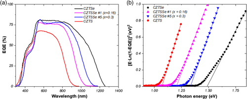
From the plot vs E and using a linear extrapolation to the x-axis (Figure 7b), it is possible to determine the bandgap of these films. Results obtained are in good agreement with the bandgap values estimated from the optical studies presented in Figure 5b.
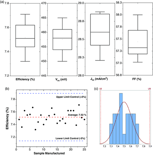
Finally, to check the reproducibility of this novel process for kesterite solar cells, champion solar cell was fabricated in a series of 25 samples. The photovoltaic parameters are shown in Figure 8a. As it can be observed, the solar cells obtained showed a performance higher than 7.2%. To analyze the reproducibility of the process, the capability process (Cp) factor was calculated, which refers to a measure of the potential capability with the assumption that the distribution of the sample process data has a normal distribution, so it represents the best process capability for the expected specifications. Considering the performance of the solar cells as the main quality indicator, Cp obtained was 1.4 (Figure 8b); according to Sig Sigma Quality Standard Procedures, this result indicates that the process is capable with high control.[46] So, the HVTD process designed and presented in this research study has demonstrated its capability to ensure a fine tune of the composition of the kesterite absorber, and its reproducibility to be scaled up for commercial applications.
4 Conclusions
A novel HVTD process was employed to prepare CZTSSe solar cells. Based on this method, the capabilities of this technique to ensure fine tuning of the absorber films composition have been demonstrated. XRF analysis revealed the equipment is able to achieve absorbers with different Cu/(Sn+Zn) ratios, from Cu-poor to Cu-rich, and different S/(Se + S) ratios, from pure selenide to sulfide structures. As a consequence, the HVTD equipment has the advantage to achieve high bandgap grading control. By controlling the (S,Se) flow gas allows the possibility to fabricate absorber layers with S-rich top and S-poor bottom configuration or homogenous depth profiles. So, the bandgap of the device can be well controlled, and when V-shape is obtained in the S content profile, the performance of the device is better. An additional electric field generated in the semiconductor enhanced the collection rate of the photogenerated carriers, reducing the motion of holes to the top and minimizing the interfacial recombination. The best efficiency obtained with this composition configuration was 7.5% under STC conditions, and it has been showed that the equipment has enough reproducibility to keep this result for a long series of samples processed. Moreover, the simultaneous selenization/sulfurization process, while these species are mixed with the metal precursors (Cu, Zn, Sn) ensuring a thermodynamic stable phase, inhibits the formation of any detrimental Mo(S,Se)2 layer. XRD and Raman spectroscopy revealed that no significant secondary phases were present on the samples, which is the main typical failure of alternative techniques using two sequential steps: deposition and annealing. These secondary phases act as defects which reduce the carrier transport and finally the performance of the solar cell.
The fast deposition rate, the temperature decoupled of the substrate and metal sources, and high control of the gas species offer a new challenge to achieve better efficiencies. Moreover, the system design combining vacuum techniques for depositing and annealing simultaneously is easy to scale up to large production.
Conflict of Interest
The authors declare no conflict of interest.
Open Research
The data that support the findings of this study are available from the corresponding author upon reasonable request.


