Tuning Electronic and Functional Properties in Defected MoS2 Films by Surface Patterning of Sulphur Atomic Vacancies
Abstract
Defects are inherent in transition metal dichalcogenides and significantly affect their chemical and physical properties. In this study, surface defect electrochemical nanopatterning is proposed as a promising method to tune in a controlled manner the electronic and functional properties of defective MoS₂ thin films. Using parallel electrochemical nanolithography, MoS₂ thin films are patterned, creating sulphur vacancy-rich active zones alternated with defect-free regions over a centimetre scale area, with sub-micrometre spatial resolution. The patterned films display tailored optical and electronic properties due to the formation of sulphur vacancy-rich areas. Moreover, the effectiveness of defect nanopatterning in tuning functional properties is demonstrated by studying the electrocatalytic activity for the hydrogen evolution reaction.
1 Introduction
Transition Metal Dichalcogenides (TMDs) are a crucial class of materials with highly attractive properties for a wide range of applications, spanning from nanoelectronics and optics to sensing and catalysis.[1] However, real manufactured materials are inherently imperfect, containing various defects that significantly influence their properties, such as vacancies, heteroatoms, boundaries, and other imperfections.[2] While these defects are often perceived negatively due to adverse effects like reduced mechanical and chemical stability and undesirable alterations in electrical transport properties, they also present numerous opportunities, enhancing and even introducing a wide range of functionalities in materials[3] The most notable example of the impact of defects in science and technology is silicon doping. Yet, a similar effect can also extend to many other materials, including TMDs.[4] Nevertheless, the interplay of various defect-generated effects can lead to drawbacks. For instance, MoS2 enriched in sulphur atomic vacancies is predicted to exhibit outstanding thermoelectric[5] and electrocatalytic properties;[6] however, the loss of electrical conductivity caused by an excess of defects limits their practical operational efficiency.[7] In this contest, defect engineering is the pivotal approach for optimising defective materials for specific applications.[8] Its primary aim is to achieve the highest sustainable defect density, maximising performance while minimising undesired effects. Over the past few decades, efforts have focused on introducing and controlling defects in TMDs, achieving reasonable control over their nature and statistical distribution.[9] However, the statistical control can only mitigate, rather than eliminate, the unwanted effects related to the conductivity.
Here, we propose surface defect electrochemical nanopatterning as a promising method to adjust the electronic and functional properties of MoS₂ thin films, avoiding undesirable effects in electrical transport properties. Surface patterning involves creating spatially defined regions with chemically active defects interconnected by pristine material areas, preserving the original materials' properties. Like an electrical circuit, pristine zones ensure efficient electrical connection between the defective but active zones through the pristine material zones, bypassing the adverse effects of defects on electrical conductivity. Additionally, patterning allows us to tune the functional properties by finely controlling the local defect density in the treated zones. These advantages are significant for thin films but become disruptive in 2D structures.
Although the advantages of spatial control of atomic defects in devices are documented in several works,[10] only a few techniques have been explored for defect patterning. These include single ion implantation,[11] scanning probe lithography,[12] electron beam lithography,[13] and focused ion beam.[14] All these techniques have proven highly efficient when applied to ideal systems such as high-crystalline flakes of MoS2. However, none fully satisfy the sustainability requirements, nanometric spatial resolution, and large operational areas needed for real technological applications, especially when applied to non-ideal systems such as polycrystalline or amorphous films.
Here, we employed Electrochemical nanoLithography (EnL) to create and precisely control high-density sulphur atomic vacancies on the surface of a MoS₂ thin film, tuning the electronic properties and generating the corresponding functionalities in a controlled manner.[3] To evaluate the effects of patterning on functionality, we investigated its effectiveness in catalysing the Hydrogen Evolution Reaction (HER), a key application of defective materials for which MoS₂ is recognised as a potentially highly efficient non-precious electrocatalyst.[6, 15]
2 Results and Discussion
2.1 Tuning of Functional Properties
- i) By controlling the local defect density. The EnL process is additive. Local VS density can be managed by altering the duration of bias application or applying the EnL process multiple times in the same region (here, we used the latter approach).
- ii) By finely controlling the patterned area. The number of VS can be regulated by adjusting the patterned area. This was achieved by applying multiple EnL processes in different areas of the samples. Increasing the patterned area increases the number of chemically active VS and, thus, the functional activity. Importantly, the defect density investigated in this study results in the range of non-interacting defects; therefore, the positions of the energy levels of the localised VS midgap remain unaffected by the defect density.
2.2 Thin Film Growth
MoS2 films were grown on highly doped silicon using sulphuration of DC sputtered molybdenum thin film, a consolidated technique largely used in industry and research.[16] This procedure allowed the growth of uniform MoS2 films on a wafer scale, offering precise control over thickness without chemical processes and minimising waste. When measured by Atomic Force Microscopy (AFM), the MoS2 surface appears homogeneous across the entire sample area, displaying a uniform distribution of nanometric grains with sizes of 25 ± 5 nm and a root mean square (r.m.s.)-roughness of 2 ± 1 nm (Figure S1, Supporting Information). Occasionally, we observed tiny crystalline zones a few microns in size and some outgrowths (i.e., large grains >10 nm thick). More details of film characterisation are reported in the experimental section and ESI.
2.3 Electrochemical Nanolithography (EnL)
To pattern MoS2 films, we used EnL, a parallel process combining scanning probe lithography[17] and lithographically controlled wetting.[18] EnL exploits an electrochemical reaction to chemically and/or morphologically modify the surfaces of substrates[19] and/or impart new functionalities.[20] Differently from other methods for electrochemical patternings,[21] such as sol-gel templates,[22] ion-conductive templates,[23] metal-organic framework template-guided electrochemical lithography[24] or a stamp as a mask,[25] EnL employs a soft conductive stamp with multiple motifs instead of a single probe to pattern spatially controlled structures on large areas in a single step. This process achieves a spatial resolution of <100 nm on surfaces larger than 1 × 1 cm2.[26] Figure 1 illustrates the schematic of the EnL process applied to MoS2 (see pictures of the actual setup in Figure S2, Supporting Information).
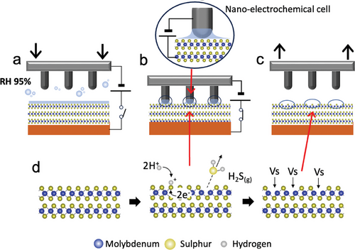
In EnL, a metallised polydimethylsiloxane stamp is carefully brought into contact with the substrate within a controlled high-humid environment (Relative Humidity ≈95%, Figure 1a). Under these conditions, a water meniscus forms between the stamp protrusions and the surface, promoted by capillary forces that create a two-electrodes nano-electrochemical cell (Figure 1b). When a voltage is applied to the substrate, local electrochemical reduction occurs. Importantly, the electrochemical reaction is confined solely to the regions underneath the stamp protrusions. This precise control forms patterned structures, reproducing the stamp features (Figure 1c). The process can be reiterated within the same zone to control the defect density, expand coverage, and create more complex structures (Figure S3, Supporting Information), tuning the functional properties.[27] Outgrowths on the sample surface act as spacers, impeding meniscus formation between stamp motifs and the surrounding surface, limiting the effective treated area (Figure S4, Supporting Information). More details about the troubles caused by outgrowths are reported in the experimental section.
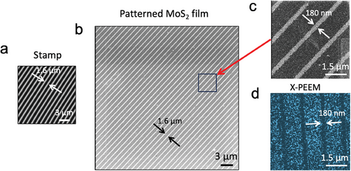
In our experimental setup, we chose a stamp with parallel lines spaced 1.5 µm (Figure 2a). This straightforward geometry effectively demonstrates our study's principles.
2.4 Scanning Electron Microscopy (SEM)
When measured by optical (Figure S5, Supporting Information) and SEM, patterned areas lack visible morphological features. To enhance surface sensitivity in the SEM images, we used beam deceleration to reduce the electrons landing energy on the sample.[29] This approach allows optimal control of the beam size and the acquisition of high signal-to-noise ratio images at 1 keV. Under these conditions, the interaction volume for generating the secondary electrons occurs within a few nm deep (usually <5nm); thus, the signal gets extremely sensitive to the surface composition and roughness. Using a decelerated electrons beam, SEM images show a clear contrast in patterned samples replicating the stamp features (Figure 2a–c); this suggests that the ENL process occurs only at the surface.
The evidence that patterned zones appear much brighter than the pristine MoS2 suggests that the contrast is due to a chemical modification, particularly an increase in the mean atomic number of the surface composition in the treated zones.[30] Notably, the contrast of low-energy SEM images increases, reiterating the EnL process in the same places (Figure S6, Supporting Information).
2.5 X-Ray Photoemission Electron Microscopy (X-PEEM)
Since conventional XPS characterisation did not show reliable differences before and after patterning (possibly because the process is limited to the surface, treating only 10%–40% of the surface area), we investigated patterned samples by synchrotron-based X-PEEM. This surface-sensitive technique combines chemical sensitivity with high lateral resolution. Figure 2d shows an energy-filtered X-PEEM image obtained collecting the intensity of the S2p core-level peak (BE ≈163 eV). The size and distance among the stripes are fully consistent with the pattern observed by SEM. According to the TPP-2M formula,[31] for incident photon energy of ≈ 400 eV, this image highlights the condition of the surface. Indeed, the decreased intensity in correspondence with the printed zones suggests the occurrence of the desulphuration process in the surface region. These observations help us to explain the contrast observed in SEM images as an increase in the ratio of Mo:S atoms due to VS formation.
2.6 Kelvin-Probe Force Microscopy (KPFM)
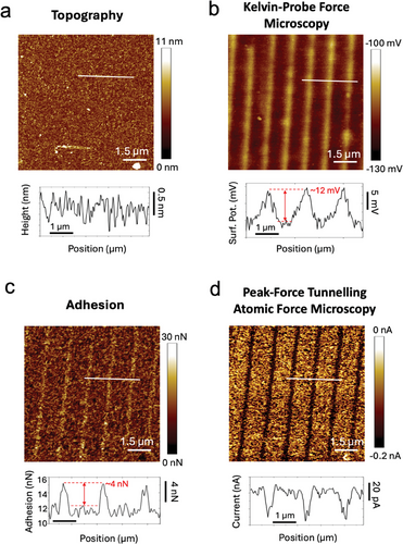
To investigate how EnL-generated defects affect the electronic properties of the MoS2 surface, we employed KPFM to probe the electrical Surface Potential (SP) of a surface, providing sensitivity to changes in the work function. Figure 3a,b presents a patterned sample's topography and corresponding surface potential image. While the topographic image has no features, the surface potential image shows a strong contrast in the printed zones. This image accurately reproduces the stamp features and displays an increase in surface potential of ≈12mV that, in our experimental configuration, indicates a reduction in work function. This reduction is attributed to the introduction of VS electronic midgap states near the conduction band edge, thereby increasing the observed surface potential. This behaviour agrees with the theoretically predicted energy change related to the mid-gap state generated by sulphur vacancies[32] and experimental KPFM investigations reported in previous works.[33]
2.7 Peak-Force Tunneling Atomic Force Microscopy (PFTUNA)
We further characterised the surface properties of the printed structures using PFTUNA, a specific variant of AFM that enables simultaneous probing of morphology, adhesion between the AFM tip and surfaces, and electrical conductivity (Figure 3c,d). Despite SPM-based measures not being evaluated quantitatively because of the complexity of the parameters influencing this type of measure, when measured by PFTUNA, patterned samples show a clear contrast in both current and adhesion values between the patterned and pristine zones. Again, the patterned zones replicate the stamp features, exhibiting adhesion values ≈5 nN higher than those in pristine areas and more than a 30% increase in the local electrical conductivity measured by PFTUNA. Two factors contribute to the enhanced electrical properties: the first is direct, due to the mid-gap states forming a lower Schottky barrier between the surface and the AFM probe.[34] The second is indirect, as VS change the surface tension. This increases the adhesion and reduces the tip-surface contact resistance, extending the tip-sample interaction time. Noticeably, no variation in electrical conductivity or adhesion force with respect to untreated MoS2 was observed between the printed lines.
2.8 Confocal Micro-Raman spectroscopy (µ-Raman)
To gain insight into the EnL process on MoS2, we used confocal µ-Raman spectroscopy to unravel the vibrational intricacies and discern the defect's nature and density.[35] The Raman spectrum of MoS2 comprises two characteristic peaks: a band at 385 cm−1 termed the and a band at 405 cm−1 termed A1g, which correspond to in-plane and out-of-plane vibrations, respectively. These bands indicate the number of layers present in MoS2 samples and the quality of the substrate (i.e., crystallinity, occurrence and type of defects). The Raman spectrum displays three primary characteristics associated with the occurrence and density of VS[35] When the VS- VS mean distance is in the range of 5–10 nm, the peak exhibits a red-shift by ≈3cm−1, while the A1g peak remains almost unaltered or exhibits a moderate blue-shift (<1 cm−1). When the average VS-VS distance decreases in the range of 3–5 nm, a new Raman peak (named LA), whose intensity is inversely proportional to the mean distance of defects, appears at 227 cm−1 (The emergence of the LA mode may also indicate the presence of disorder in MoS2). Eventually, when the average VS -VS distance falls below 3 nm, the and A1g peaks broaden proportionally to the mean VS-VS distance reductions. Figure 4a illustrates the Raman spectra of a patterned MoS2 before (pristine) and after EnL patterning. The prominent peak in the Raman spectra at 301 cm−1 is attributed to Raman scattering from the silicon substrate.[36]
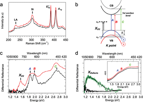
Upon EnL patterning, for coverages > 20%, the LA peak, at 227 cm−1, distinctly emerges in the spectra without relevant change in the and A1g peaks. This change, associated with desulphuration observed in XPEEM measurements and the formation of the mid-gap states, allows us to estimate the formation of VS with an average VS -VS distance of ≈ 4 ± 1 nm.[35] However, we cannot exclude the contemporaneous formation of local disordering in the MoS2 lattice.
The evidence that the LA peak is observed only in the samples which have undergone multiple EnL applications suggests that this density of VS is probably reached only in the zones treated at least two times. No evidence of Raman spectra alteration was observed in the samples' untreated zones.
2.9 Micro-Differential Reflectance Spectroscopy (µDR)
The effect of EnL patterning on the electronic structure was investigated using µDR, an effective method for probing, with high sensitivity, the surface optical absorption and for studying electronics in thin semiconductor films.[37] Figure 4b shows the schematics of the low-energy band structure, at K point, of a crystalline MoS2 film containing isolated atomic sulphur vacancies.[38] The two spin-orbit coupling split bands, A and B, characterise the optical absorption. These are transitions from the maximum of two Valence Bands (VB, red and blue) of opposite spin to the degenerate first exciton level at the Conduction Band (CB) minimum. Δ is the valence band splitting energy (Δ≈0.15 eV). C band is associated with transitions between VB and CB, and it is strongly thickness dependent. VS results in a single state (occupied level, vD) below the VB and two nearly degenerate (unoccupied) states (cD1 and cD2, are indicated as cD) in the gap. Lowest energy transitions XD1,A, XD1,B and XD2,A, XD2,B have very low intensity. Conversely, the XD2 band (between occupied and unoccupied defect levels) exhibits an intensity related to the amount of surface defects, and it can be used as an optical benchmark to monitor the VS density. Here, only spin-up defect transition is indicated. Figure 4c shows (black curve) a paradigmatic absorption spectrum of crystalline MoS2 flakes according to this scheme. The spectrum exhibits the two sharp bands “A” (≈1.85 eV) and “B” (≈1.99 eV) and a broadband “C”, cantered at 2.70 eV, indicating a flake thickness of 2–3 monolayers.[37] Figure 4c (red curve) shows the µDR spectrum collected from the surfaces of one of the patterned films (patterned area: ≈40%) with respect to the untreated surface. The signal was acquired from a selected crystalline region (diameter ≈30 µm) of the patterned film immediately after the EnL process and was compared with the absorption of the MoS2 crystalline flake. The presence of residual spectral modulation in patterned samples (A and B bands are convoluted) is due to the poor crystallinity of the area of the pristine MoS2 film used as a reference compared to the patterned one. At the same time, the appearance of several variously shifted C bands is related to the distribution of thicknesses of MoS2 crystallites inside the observed area of the patterned film.[39] Differently from the MoS2 flakes, which are apparently transparent in the spectral region below the first excitonic transition (A), the differential reflectance of the patterned film exhibits a large, well-defined band centred at ≈1.54 eV (λ≈805 nm). We associate this band with the direct transition XD2 at the K point (Figure 4b).[38] More generally, XD2 has to be interpreted as a weighted overlap of transitions both from the valence band maximum and from the occupied defect level vd to the mid-gap unoccupied defect band cd. Indeed, this is direct experimental evidence of the formation of localised, unoccupied, in-gap states associated with EnL desulphuration. This result is consistent with the predictions from many theoretical studies[40] and other experimental observations.[32, 38, 39] Noticeably, the emergence of optically accessible states by the EnL process indicates that it generates an unoccupied mid-gap state. Importantly, exposure to light in the air causes this band to become unobservable within a few hours after the sample preparation, likely due to vacancies being filled by oxygen atoms.[32, 41] However, in poorly crystalline patterned regions, the MoS2 mid-gap states are usually undetectable even by µDR (Figure 4d, black squares). Moreover, the absorption spectra of these films are much less structured (Figure 4d, inset). Nevertheless, upon treatment with bis-(trifluoromethane)-sulfonimide lithium salt (Li-TFSI), an agent employed to deplete the occupied VS states in defective MoS2,[32] a very broad band appears inside the bandgap (Figure 4d, green curve), demonstrating the depletion of existing mid-gap states.
2.10 Correlation between Patterning and Electrocatalytic Properties
To evaluate the correlation between patterning and functionalities, we tested their effectiveness in catalysing the hydrogen evolution reaction (HER) in acid media, a critical application for which MoS₂ is recognised as a potentially highly efficient non-precious electrocatalyst.[6, 15] Although we are aware that the application of patterning in catalysis is not particularly advantageous in terms of absolute performance if compared to globally treated samples, we considered this functionality because of its importance in TMDs application and because it is remarkably efficient to demonstrate that defects produced by EnL are chemically active and can be modulated, delivering performance comparable with the state-of-the-art.[15] Our preliminary investigation focuses on discerning the impact of nanopatterned chemically active VS on electrochemical activity pertinent to HER in acid media. We investigated various samples featuring diverse geometries and percentages of patterned areas (0%, 10%, 20%, and 40%), achieved through multiple iterations of the EnL process (details in experimental sections). Figure 5a shows that Linear sweep voltammetry (LSV) curves of patterned MoS2 films have a higher current density (J) than pristine MoS2 (see Tafel slop in Figure S8, Supporting Information).
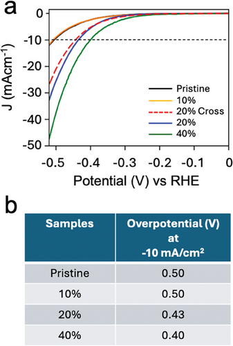
The observed activity in pristine MoS₂ is likely due to inherent defects within the film. The LSV curves show a strong correlation between HER electrocatalytic activity and the degree of patterning, confirming that the EnL process generates catalytically active sulfur vacancies. Areas with greater treatment exhibit enhanced activity. Notably, samples with 40% treated areas displayed significant electrocatalytic performance, with an overpotential of −0.40 V at a current density of 10 mA cm⁻2. In contrast, while occasional improvements were observed, samples with only 10% treated areas generally showed behaviour similar to untreated MoS₂, suggesting that substantial enhancement in electrochemical activity occurs only when the treated area exceeds 10%. We attribute this behaviour to outgrowths in the MoS₂ films, which introduce significant variability in the actual coverage of patterned areas. The extent of untreated regions depends on the thickness of the outgrowths, which leads to a marked reduction in the effective patterned area. This effect is more pronounced when the EnL process is applied once (see Experimental Section). The table in Figure 5b reports the details about the trend of overpotential at different coverages.
When comparing the LSV curves of patterned samples with different geometries (e.g., parallel lines printed twice and crossed lines; see methods and Figure S5, Supporting Information), there were no macroscopic differences in electrocatalytic performance (Figure 5). However, some differences were observed at low current values (Figure S7, Supporting Information), suggesting possible effects of defect density and pattern geometry on electrocatalytic mechanisms. Specific studies on this topic are currently underway.
It is worth noting that although EnL-treated MoS2 films exhibit enhanced electrocatalytic activity (>5 times at −0.5 V vs RHE, Figure 5a), our samples have limited performance compared to conventional MoS2 electrodes.[42] This is because our systems consist of models with almost flat surfaces, with surface areas orders of magnitude smaller than the porous architectures employed in energy conversion and storage devices.
3 Conclusion
In summary, this work introduces a practical method to fabricate a spatially controlled distribution of VS in MoS2 thin films. We demonstrate the remarkable potential of spatially controlled defect manipulation, specifically through EnL, to generate and tune the electronic and functional properties of MoS2 surfaces. Our comprehensive set of analytical techniques underscores the versatility of electrochemical patterning for nanoscale defect engineering. The results demonstrate that EnL enables spatial control with remarkable resolution in the submicrometric range confined to the surface. Confocal µ-Raman spectroscopy, KPFM, µDR, and X-PEEM measurements confirm the formation of atomic vacancies only in the desired zones, generating unoccupied midgap states. Furthermore, we assess the electrocatalytic properties of MoS2 films for the hydrogen evolution reaction, revealing that the spatial distribution of VS-rich printed zones enhances the electrocatalytic activity in HRE, with an improvement of more than five times compared to untreated MoS2. Our study significantly contributes to the advancement of defect engineering in MoS2 and highlights its critical role in science and technology. The ability to control defects with nanoscale precision opens new possibilities for tailoring material properties to meet specific requirements in electronics, including 2D devices, catalysis, and optoelectronic applications. Here, we use MoS2 films as a representative material, but this process can easily be extended to other semiconducting materials. As we unravel the intricacies of defect engineering, our findings pave the way for further advancements in designing and optimising materials for diverse technological applications.
4 Experimental Section
Thin Film Preparation
A molybdenum thin films were deposited via D.C. pulsed magnetron sputtering in a homemade system capable of processing large-area substrates (up to 9 × 9 cm2). Before the depositions, the highly doped silicon substrates were carefully cleaned in an ultrasonic bath with the following sequence: mucasol solution (15′), deionised water (2 × 15′), acetone (15′), and ethanol (15′), and singularly dried under nitrogen flow.[43]
In a high vacuum chamber (base pressure 200µPa), Mo was deposited at the Ar working pressure of ≈ 0.6 Pa with the fixed sputtering current of 1A (powers of 261W) using high-purity Mo targets (5 N). The different layers’ thicknesses were obtained by changing the sputtering time. In this work, Mo thin film 5–6 nm tick was used. The MoS2 thin films were obtained by a sulphuration process using a tubular oven.[44] Mo thin films were placed into a tubular quartz reactor using a quartz shuttle equipped with a silicon wafer slice acting as a sample holder (to avoid direct contact with the quartz surface). A graphite crucible containing adequate Sulphur was housed next to the samples. The tubular quartz reactor was maintained under an inert atmosphere (Ar), and the temperature was raised from RT to 465 °C with a rate of ≈ 16 °C min−1, followed by a plateau at 465 °C for 20 min. Subsequently, the tubular quartz reactor was removed from the oven and was left to cool down naturally under Ar until RT. Thin films were characterized using X-ray photoelectron spectroscopy (see Supporting Information), atomic force microscopy and Raman spectroscopy.
Li-TFSI Treatment (used only for Differential Micro-Reflectance Spectroscopy Measures)
MoS2 films are treated in a (0.02 m) solution of bis(trifluoromethane)sulfonimide lithium salt (Li-TFSI) in methanol for 40 min at room temperature to passivate the VS formed during the electrochemical exfoliation process. They are then annealed in Ar for 1 h at 300 °C to remove possible organic residues from the film. Figure S1 (Supporting Information) shows an AFM image of MoS2 film.
Electrochemical Nanolithography (EnL)
The EnL process was performed using a homemade apparatus described in detail (ref.[19]). A commercial hygrometer controls relative humidity. The real extension of the patterned area is strongly influenced by the density of outgrowths on the films. Outgrowths act as spacers and impede the meniscus formation between stamp motifs and the surrounding surface. The extent of the untreated area is contingent upon the outgrowth thickness, leading to a substantial reduction in the patterned area.
Considering the presence of outgrows, we estimated from large area analysis that in our films, the application of ENL one time using a stamp made of parallel lines spaced 1.6 µm, patterns 10 ± 2% of the surface area; the application of ENL 2 times, rotating the stamp 90°, patterns 20 ± 4% of the surface area (n.b.in this case ∼2% of the surface, in correspondence of the crossed zone is treated two times); the application of ENL 4 times (rotating the stamp 45°, 90°, 135°) patterns ≈40 ±8% of the surface area (n.b. in this case ≈4% of the surface in correspondence of the crossed zone is treated at least two times).
Stamps
The elastomeric polydimethylsiloxane (PDMS, Sylgard 184 Down Corning) stamps were prepared by replica moulding. The curing process was carried out for 1 h at 70 °C. Once cured, the replica was peeled off from the master and washed in pure ethanol to remove the uncured polymer.[45] The metallic film of commercial blank compact disks was directly used as a stamp. The stamp motif consists of parallel lines with a periodicity of 1.6 µm, a width at the apex of 200 nm and a depth of 220 nm (Figure 2a in the text).
Scanning Probe Microscopy (AFM, KPFM, PFTUNA)
A Bruker Multimode 8 microscope was employed for all the scanning probe microscopy characterizations. All the measurements have been carried on in air at ambient conditions. For the Kelvin probe force microscopy (KPFM) measurements, the amplitude modulated (AM) tapping mode was employed, which is a two-passage lift mode (we use a lift height of 20–50 nm without difference in the observed signal). To a first approximation, KPFM measures the surface potential SP of the sample, which can be directly related to the work function via the simple formula SP = │WFtip│–│WFsample│, where WFtip is the known sample's work function. The Peak-Force Tunneling Current Microscopy -PFTUNA- module from Bruker was employed to measure simultaneously qualitative mechanical properties (i.e., the adhesion) and the electrical current passing from the substrate to the tip through the sample. We used a Bruker “SCM-PIT-V2” probe (f = 75kHz, k = 3N m−1, material: n-Si) for AM-KPFM and a Bruker “PFTUNA” probe (f = 70kHz, k = 0.4N m−1, material: Pt-Ir coated Si3N4) for PFTUNA measurements. We performed image processing to correct piezo-scanner artefacts with SPIP software.
Specifically, topographic images shown in the main text are corrected with global plane levelling. For graphical reasons, Kelvin probe images have been corrected with a line-wise plane levelling. For the same reason, Adhesion and Current maps have been corrected using a noise reduction and local smoothing filter. Corresponding non-filtered images are shown in Figure S3 (Supporting Information).
X-Ray Electron Spectro-Microscopy (X-PEEM)
X-PEEM was performed at the I06 beamline at DIAMOND Light Source using an Elmitec Gmbh X-PEEM equipped with an electron energy analyzer. Samples were probed at room temperature and a base pressure of 1e-9 bar. No in-situ treatment was performed. The X-PEEM images (field of view 15 mm) were obtained by collecting the intensity of secondary electrons of the core-level S2p peak. For graphical reasons, the W-PEEM Image shown in the text was treated by optimising the contrast and applying a smoothing routine. Corresponding non-filtered images are shown in Figure S8 (Supporting Information).
Scanning Electron Microscopy (SEM)
SEM images were acquired using a TESCAN GAIA3 2016 scanning electron microscope, which also includes an ion column. The images were captured in beam deceleration mode, with the column set to operate at 6 keV and an applied bias to the sample to achieve an electron landing energy of 1 keV. The working distance was maintained at 5 mm, and the secondary electron signal was recorded using an in-column secondary electron detector.
Raman Spectroscopy (µ-Raman)
µ-Raman spectra were recorded in backscattering geometry through a Renishaw1000 system using the 514.5 nm (2.41 eV) Ar+ laser line through a × 100 objective lens with a spatial resolution of 1 µm. To avoid local heating of the films, laser power was kept at 80 µW.
Differential Optical Reflectance (µDR)
Differential optical reflectance spectra were recorded using a modified Nikon EnLipse80i microscope.[46] The trinocular turret was customised to use a home-made optical system composed of a 50mm focal quartz lens focused into an optical Vis-iR fibre (Thorlabs) to feed the optical signal from the microscope into an Avantes AvaSpec-2048 CCD spectrometer (2048 pixels array, DLC UV/Vis, 200–1100nm range, 10µm entrance slit, software programmed). This setup allowed us to acquire optical images and collect the transmitted signal from the sample under a 20X-100X objective. We used the built-in Nikon halogen lamp (working illumination range 360–1200nm) as light source. The lamp light was brought and focused to the sample surface by the microscope optics. The reflected signal collected back across the same objective was then fed into the spectrometer via optical fibre. It was then possible to select the more suitable zones by visual inspection to measure the local reflectivity in a region with a minimum size of 10 × 10 µm2.
Electrocatalysis
Acknowledgements
The authors thank the European Union funded this research – Next Generation EU from the Italian Ministry of University and Research. Project PRIN 2022SRHPF2 ″Molecular assisted atom vacancies arrangement to modulate magnetism in 2D transition metal dichalcogenides″ (MAVAM) and Italian Ministry of Environment and Energy Security POR H2 AdP MMES/ENEA with involvement of CNR and RSE, PNRR – Mission 2, Component 2, Investment 3.5 ″Ricerca e sviluppo sull'idrogeno″. V.B. was financially supported by the H2020-MSCA-ITN ULTIMATE (grant number 813036). S.A.M. acknowledges a Ph.D. scholarship on Green Issues from action IV.5 of the PON Research and Innovation 2014–2020 ″Education and research for recovery – REACT- EU″ program. C.S. would like to thank the support from ENEA – UNIMIB agreement (Procedure 1.1.3 PNRR POR H2); G.C. was supported by Project ECO SISTER – Ecosystem for sustainable transition in Emilia-Romagna, PNRR Mission 4, Component 2, Investment 1.5, ″Creazione e rafforzamento di ″Ecosistemi dell'innovazione″.
Open access publishing facilitated by Consiglio Nazionale delle Ricerche, as part of the Wiley - CRUI-CARE agreement.
Conflict of Interest
The authors declare no conflict of interest.
Author Contributions
D.G., E.L., F.B., and G.C. contributed equally to this work. M.C., A.L., M.A., C.S., A.C., F.B. conceived the experiments and wrote the paper. D.G. and G.C. performed the patterning process and contributed to sample characterisation, G.T. and S.A.M. grew the films and pursued the sulphuration process, and A.M. (XPS), S.A.M. (Electrocatalysis), V.B. and A.C. (AFM, KPFM, TUNA), G.R. (µ-Raman) characterised samples. F.B. and F.M. performed X-PEEM synchrotron radiation experiments and analysed the data. E.L. performed differential optical reflectivity characterisation. V.P. supervised V.B.'s activity and contributed to the discussion F.L. supervised G.C.'s activity and contributed to the discussion. All authors discussed the results, commented on the manuscript, and prepared written contributions. The manuscript was written through the contributions of all authors. All authors have approved the final version of the manuscript.
Open Research
Data Availability Statement
The data that support the findings of this study are available from the corresponding author upon reasonable request.


