Silver Nanocube Epitaxy via Nanogap-Induced Electrostatics
Abstract
Silver nanostructures are highly valued in nanophotonic devices due to their appealing plasmonic properties and affordability relative to gold. Yet, fabricating high-quality, monocrystalline silver nanostructures, with full control over the shape, is challenging. A mild, liquid-phase method for the epitaxial welding of adjacent monocrystalline silver nanocubes in reductant-free conditions is introduced to prevent the formation of detrimental nuclei on the surface that can degrade the nanostructures' optical qualities. The mechanism is thoroughly investigated and it is found that the nanocubes themselves can act as reducing agents, promoting growth preferentially into the gap as a result of electrostatic interactions. By controlling experimental parameters such as temperature, pH, and the introduction of capping agents, a balance between nanocube epitaxy and shape retention is achieved. Finally, by applying this procedure to nanoparticle assembled in predefined meta-atoms, the feasibility of creating intricate silver nanostructures, that are monocrystalline as verified by transmission electron microscopy (TEM), is demonstrated. This advancement paves the way for bottom-up fabrication of optical metasurfaces that can be swiftly integrated in devices.
1 Introduction
Introduction. The interest of silver nanostructures for nanophotonic devices stems from their appealing plasmonic properties and cost-effectiveness compared to gold. However, achieving low-cost fabrication of the highest-quality monocrystalline silver nanostructures with arbitrary shapes remains a significant challenge. Meanwhile, the importance of single-crystalline grade nanostructures in such devices has been reported by many.[1-6] One approach for fabricating monocrystalline structures of arbitrary shapes involves substrate-based epitaxial growth, which produces single crystalline thin films that are then nanostructured using lithography processes such as electron beam lithography (EBL). Yet, this method's demands for high temperatures and/or high vacuum, and lattice-matched substrates,[6] combined with the high costs and time requirements of EBL, that also introduces defects due to etching, further complicates fabrication. This challenge, therefore, spurred research into directed assembly of nanoparticles that allows their placement in desired locations on a substrate with high fidelity.[7-9] However, this method still results in the assembly of discrete nanoparticles separated by capping agents and gaps that prevent direct electrical contact and extended monocrystalline complex structures, thereby restricting the full exploitation of the shape-dependent plasmonic properties.[9-12]
While the monocrystalline quality of interconnections formed through nanowelding has been previously investigated in systems such as quantum dots,[13] metallic nanorods,[14] and 2D semiconducting nanoplatelets,[15] the interplay between nanowelding quality and the flexibility to design arbitrary geometrical arrangements in nanoparticle assemblies was not largely addressed. Several studies have presented various strategies for connecting assembled metal nanoparticles, including nanorods assembled in meshes sintered through plasma treatment,[16-19] nanospheres assembled in grids through photochemical welding,[20] clusters of nanospheres assembled in dot arrays sintered through thermal annealing[21, 22] and in rings through chemical welding.[23, 24] These approaches focus primarily on the interconnection process itself, with limited attention to other critical aspects such as the crystalline quality of the connections or the retention of precise shapes in nanostructures with sub-100 nm features.
One approach to address this challenge involved transforming substrate-supported silver nanocubes into monocrystalline nanorods using a solution-based chemical synthesis.[25] Employing a Tollens' reagent based on glucose as reducing agent for a diamminesilver(I) complex, this process promoted nanocubes overgrowth and their epitaxial connection. However, this also led to unwanted homonucleation in solution and heteronucleation on the substrate, which can impact the final nanostructures' overall quality. The development of chemical procedures that avoid the use of exogenous reducing agents appears to be the most effective strategy for suppressing entirely unwanted nucleation, but encounters challenges in solution-based processes, where metal sources are typically in ionic forms. We recently reported an effective approach to weld gold nanocubes, relying on the migration of gold atoms from corners into gaps through dissolution and redeposition via a disproportionation reaction, which entirely suppresses unwanted nucleation.[26] Unfortunately, this reaction is unique to gold and it is not readily transferable to other metals such as silver.
Inspired by this concept of welding via the rearrangement of surface atoms, we investigate a new synthetic framework to achieve epitaxy between silver nanocubes without using an exogenous reducing agent, thereby overcoming the nucleation issues associated with previously reported overgrowth strategy. We show that this approach is compatible with various supports including nanopatterned polydimethylsiloxane (PDMS), hence enabling the integration of intricate monocrystalline silver nanostructures onto new substrates via contact printing.
2 Results and Discussion
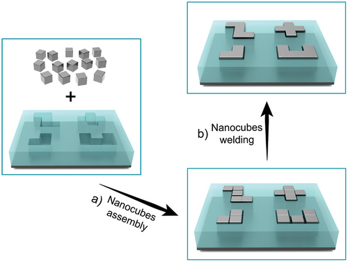
Figure 1 provides a general overview of the strategy to obtain monocrystalline meta-atoms with a truly arbitrary geometries. First, silver nanocubes are assembled into nanopatterned trenches of various shapes realized in a PDMS substrate using reported techniques, either capillary-assisted assembly[26] or air-water interface assembly.[27-29] The former technique involves dragging a colloidal solution over a nanostructured PDMS mold, trapping nanocubes within the trenches at the meniscus front line, driven by convective flow from solvent evaporation.[26] Alternatively, the latter technique transfers a dense monolayer of nanocubes from the air-water interface onto the nanostructured PDMS template, where a fraction of nanocubes is trapped in the trenches while the excess is deposited outside. Removing the excess leaves behind only the nanocubes assembled within the patterned trenches.[27] These techniques position the cubes face-to-face within the trenches, matching the trench geometry (Figure 1a) and imposing identical crystallographic orientation of the nanocube building blocks thanks to their 4-fold rotational invariance. Subsequently, epitaxial welding in solution results in extended continuous monocrystalline polyomino-like nanostructures (Figure 1b), which can then be transfer-printed onto other substrates, if required.
To design and investigate a suitable chemistry for the reductant-free epitaxy of silver nanocubes, we first started with randomly assembled aggregates, achieved by drop-casting monodisperse silver nanocubes (with size ranging from 30 to 70 nm) onto silicon substrates. The distance between face-to-face nanocubes depends on the ligand thickness and is typically in the order of a few nanometers.[30] We then removed the polyvinylpyrrolidone (PVP) ligands from their surfaces using a previously reported procedure[31] (described in the experimental section). After ligand removal, the nanocubes moved closer to one another due to van der Waals attractions and/or capillary drying forces, reducing the average gap size from ≈1.8 to ≈0.7 nm (Figure S15, Supporting Information). While the removal of ligands did not immediately induce welding, ligand-free silver nanocubes, which are chemically and thermally less stable than their gold counterparts, gradually merged and interconnected when immersed in deionized water at room temperature over three days, as shown in Figure S1 (Supporting Information). This indicates the presence of a driving force toward the formation of continuous structures. While the free energy of the system is reduced in this process (the disappearance of the two surfaces corresponds to a 17% reduction of the initial surface area considering a two-particle system), the activation barrier is sufficiently high to prevent welding in a time scale of a few hours. Regardless of the kinetics, for this to happen, it is necessary that Ag atoms are displaced into the gap. Despite surface diffusion of metal atoms can be fast, it is not sufficient to trigger the welding process as it would require anisotropic diffusion of electrically-neutral species.
Previous studies have shown that silver atoms in low-coordinated sites,[26, 32-34] such as cube corners, oxidize at a higher rate to Ag+ ions in solution under oxidative dissolution conditions due to higher surface energy. This can leave behind excess electrons in the nanocubes inducing the formation of a dynamic ionic layer at their surface and in the gap as a result of Coulomb interactions. We hypothesize that in the gap, the overlap of diffuse layers and the modified electrostatic interactions (compared to an isolated nanocube) result in the accumulation of Ag+ ions. This higher concentration in the gap makes it a privileged location for the reduction of Ag+ ions to Ag adatoms, with electrons sourced directly from the excess present in the nanocubes themselves. This process is thermodynamically favoured as it leads to a reduction in the free energy of the system due to the decrease in surface-to-volume ratio after welding is achieved (loss of two surfaces). This heuristic analysis is corroborated qualitatively by multiphysics numerical simulations coupling electrostatics with the transport of charged species on a simplified nanocube-dimer model. Figure 2 shows the spatial distribution of the cation concentration, normalized by its maximum value, C/Cmax, for various gap sizes. The net charge corresponds to the excess electrons in each nanocube, and correspondingly to the excess cations in solution in addition to the self-dissociation of water. Two different scenarios of net charge present on the nanocubes are considered, corresponding to 1q (left panel) or 3q (right panel), where q is the elementary charge. These scenarios are established to unveil the impact of the gap in limiting experimental conditions corresponding to one or a few excess electrons only, which can be a realistic condition especially in the early stages of the oxidation process. The resulting electrostatic field attracts opposite mobile charges such as cations in solution. Figure 2 shows the steady-state configuration, at which point the excess charge in the nanocubes is balanced by ions present in the simulation domain.
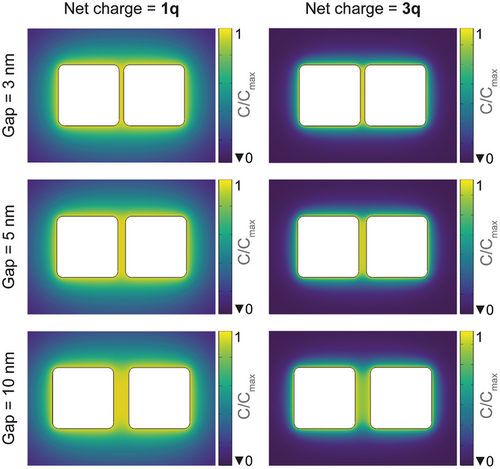
These results confirm, qualitatively, the accumulation of positive ions in the gap as a result of the concerted electrostatic action of the charged nanocubes, supporting our hypothesis. Finally, it is worth noticing that this concentration effect in the gap is enhanced with smaller gaps and larger excess charge. The dependence on the charge amount is related to the Boltzmann distribution of the ion concentration profile near an electrically charged surface, in which there is an exponential dependence with the surface potential (Poisson–Boltzmann equation). Although the purpose of this comparison is merely qualitative, we believe it sheds light on the mechanism.
Using this spontaneous transformation as a starting point, we aimed to improve the welding kinetics and the shape retention on PDMS-supported nanocubes. We hypothesized that, in addition to temperature, the concentration of Ag+ ions is key for a faster kinetics. We used diluted HNO3, a known silver etchant,[35, 36] to oxidize Ag atoms in low-coordinated sites (see next), thereby increasing the availability of Ag+ ions in solution. This significantly accelerated the transformation compared to water, as illustrated in Figure 3a,b. Additionally, conducting the reaction in water at elevated temperatures facilitated the merging of some face-to-face nanocubes into continuous structures more rapidly (shown in Figure 3c), although the impact of temperature alone was rather limited.
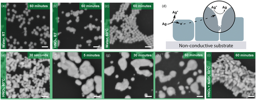
Combining higher temperature with HNO3 further increased reactivity, resulting in excessive nanocube etching and the emergence of 3D structures within an hour (Figure 3e–h). Notable differences in samples immersed in the welding solution for 30 s, 5 min, and 30 min demonstrate that the reaction is not self-limiting and tends toward nanocube rounding (Figure 3f) and dissolution (Figure 3g,h), as it is evidenced by the presence of nanoparticles definitely smaller than the original nanocubes. Gap size certainly plays an important role in the welding reaction, but quantitative investigations are challenging due to the approaching of nanocubes to one another after ligand removal as a result of van der Waals interactions and drying capillary forces (Figure S15, Supporting Information). It is important to emphasize that the reaction takes place in the absence of a silver salt, implying that all silver atoms filling sub-nanometer gaps must come from the nanocubes themselves, as mentioned earlier. This contrasts with the welding of gold nanocubes, which requires the presence of a gold precursor,[26] and highlights a striking difference in reactivity. This is supported by the comparison of the work functions and the redox potentials of the two metals (indicated in the Supporting Information). Such metrics clearly indicate that electron extraction and therefore metal dissolution is significantly easier on Ag than Au. As shown in the Pourbaix diagram (Figure S2, Supporting Information), water, and even more so HNO3, can induce Ag oxidation to Ag+. The diagram also shows the vast stability domain of the cation in aqueous solutions (see also calculations in Figure S2, Supporting Information).
To investigate the silver dissolution at the nanocube surface, we performed electrochemical experiments on bare or silver-coated glassy carbon (GC or GC-Ag, respectively) immersed in Ag-free or Ag-containing solutions (see Supporting Information for more details). Figure S4a (Supporting Information) shows cyclic voltammograms (CVs) performed on GC and GC-Ag in diluted HNO3. As expected, when GC is exposed to HNO3, it exhibits no reactivity. As a result, only a weak current density is measured. Conversely, electrochemical activity is observed on GC-Ag, displaying anodic and cathodic peaks centered at −0.7 and −0.56 V corresponding to the dissolution and deposition of silver, respectively.
In the case of GC-Ag in HNO3 (Figure S4a, Supporting Information), the curve shows that Ag+ ions are present in the solution as soon as the electrode is immersed. The cathodic peak observed at −0.7 V indicates the reduction of Ag+ to Ag. However, during the cyclic voltammetry, the potential is first scanned negatively from open circuit potential (ocp ≈ −0.45 V), then toward positive voltages and, finally, back to the starting value. The observation of the cathodic peak at −0.7 V demonstrates that Ag+ is present although no anodic polarization has been applied to strip the silver film covering the GC. It is the spontaneous silver dissolution that induces the presence of cations in the solution. A similar process occurs on nanocubes. The dissolved Ag+ can then be redeposited at their surface preferentially in the gaps where Ag+ concentration is higher. The CVs presented in Figure S4 (Supporting Information) also indicate that the overvoltage (η that corresponds to the difference between ocp and the onset potential for Ag+ reduction) is relatively small (η = 33 to 165 mV depending on the experimental conditions). It demonstrates that the energy requested for the Ag deposition is low. The reduction peak is even further positively shifted when closely packed Ag nanocubes are assembled on the glassy carbon (GC-cubes, see Supporting Information for more details). Figure S5 (Supporting Information) compares CVs performed on GC-Ag and GC-cubes in 0.01 M HNO3. The cathodic peak attributed to Ag+ reduction (* on the CV) is centered at −0.58 V (while it is −0.7 V for GC-Ag) and the onset potential for Ag+ reduction is difficult to assign because negative current starts already from ocp. This is in line with the under potential deposition (UPD) reported for silver on single crystalline metals such as Pt.[37] Since Pt lattice is very close to Ag, UPD should proceed even more easily on Ag (100) facets of the nanocubes. Note also that the anodic peak ( on the CV) corresponding to silver stripping is positively shifted to −0.1 V. This suggests that dissolution of redeposited silver is more difficult, as it occurs mainly on the (100) facets facing each other in the gaps between the cubes.
The high reactivity of atoms at nanocube corners, due to higher surface energy sites,[32, 33] results in their faster dissolution and the transformation of nanocubes into nanospheres at long reaction times, as observed in Figure 3h. Silver atoms on different sites on a single nanoparticle or on nanoparticles of different sizes, might present slightly different reduction potentials arising from differences in surface energy. Consequently, when nanoparticles on a substrate are immersed in a solution, they tend to reorganize by oxidizing at high-energy sites and redepositing (reduction) at more stable locations according to the electrochemical processes described above. This can be facilitated by electron transport through the substrate (if conductive – see next) or by tunneling between neighboring nanoparticles (for sub-nanometer gaps), moving from high-energy to lower-energy sites to initiate Ag+ reduction, as depicted in Figure 3d and Figure S6d (Supporting Information). This mechanism, previously reported as electrochemical Ostwald ripening,[38] has been used to grow silver on conductive substrates using water only, as a result from smaller nanoparticles dissolving to the benefit of larger nanoparticles. In addition, it was reported that this transformation is exacerbated by acidic conditions and in the presence of silver ions.[38, 39]
To improve shape retention, we added micromolar concentrations of NaBr to the welding solution, as bromide ions can selectively adsorb on (100) facets, reducing their surface energy and growth rate.[26, 40, 41] After systematic parameter variation, we found (on flat PDMS) an optimal balance between rapid kinetics and shape preservation by conducting the reaction at 60 °C, pH = 2 with 50 µM NaBr, as shown in Figure 3i.
Welding experiments on various substrates, including silicon, revealed that while the impact of different parameters was similar, the optimal conditions varied slightly (Figure S6, Supporting Information). This is further evidenced in Figure S7 (Supporting Information), which demonstrates that silver nanocubes, when exposed to the same welding solution on diverse substrates like untreated silicon, UV/ozone-treated silicon, glass, and Si3N4, showed varying degrees of welding. Notably, nanocubes on untreated silicon and Si3N4 underwent more extensive welding compared to those on glass, where oxidative etching was less pronounced, and on ozone-treated silicon, where silver deposition in the gaps appeared to be inhibited. This variability likely stemmed from the substrates' unique surface chemistries, which can affect ion diffusion through electrostatic interactions or participate in the reaction through surface oxidation. This is particularly relevant for conductive substrates like silicon, in addition to the role of electron conduction.
Next, this approach was implemented to silver nanocubes arranged in nanopatterned PDMS trenches, and demonstrated its potential to obtain intricate monocrystalline meta-atoms. It was discovered that the welding process was affected by the confined environment of the PDMS trenches, having lateral dimension comparable to that of the nanocubes. In these trenches, the diffusion of reactants introduced is notably altered and the availability of Ag+ ions is limited due to the significantly lower nanocube density compared to when they are drop-casted. Identifying the ideal conditions to achieve seamless continuous nanostructures without compromising the nanocubes' morphology proved challenging, as excessive dissolution or insufficient welding were encountered when adjusting the Br− concentration.
To mitigate this issue, an alternative strategy was explored by adding millimolars concentration of a silver salt (CF3COOAg). This addition proved effective to significantly enhance shape retention and enabled the formation of continuous 1D nanostructures with varied aspect ratios, as demonstrated in Figure 4a,b displaying nanorod arrays welded together. Figure S14 (Supporting Information) further illustrates large-area welding of nanocube dimers obtained by capillary assembly.[42] In efforts to understand the underlying mechanism, control experiments conducted in dark conditions, which showed outcomes consistent with those obtained under normal lighting conditions, eliminated the possibility of light-induced silver reduction (Figure S8, Supporting Information). In contrast, using AgNO3 as a silver source intensified the etching process due to the generation of HNO3.[43] It is noteworthy that tests with 10 mM CF3COONa (Figure S9, Supporting Information) showed that CF3COO− ions did not contribute to shape preservation. Despite calculations suggesting no attainable equilibrium between oxidation and growth at high silver ion concentrations, we speculate that a higher concentration of Ag+ ions increases the likelihood of interaction, leading to their reduction via the excess electrons in the nanocubes, in accordance with the observations presented earlier.
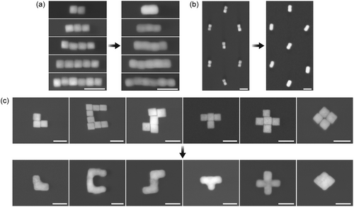
Using air-water interface assembly technique,[27] we successfully arranged nanocubes into more intricate geometries. This allows us to further test the potential of this welding approach to 2D meta-atoms. Figure 4c showcases the formation of continuous nanostructures from 55 nm silver nanocubes, including L, C, S, T, +, and a 2×2 nanocube square shapes. This highlights the method's adaptability in welding tightly packed nanocubes into various arrangements, with the trench geometry playing a crucial role in defining the meta-atoms' final shape. Additionally, Figure 4 confirms the absence of nanoparticle nuclei on the surface resulting from homonucleation, showcasing the superiority of this new chemical strategy over traditional overgrowth techniques. The dark-field scattering spectra before and after nanowelding are shown in Figure S16 (Supporting Information).
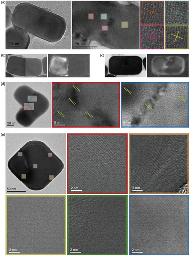
Finally, the crystallinity of the welded nanostructures was verified by TEM, shown in Figure 5a,d,e. These images reveal that structures, ranging from 1D rods to a more complex 2D L-shape or diamonds, are monocrystalline, as confirmed by the presence of continuous atomic columns or planes across the nanocube junctions, despite some contrast can be observed in some locations. Dislocations, as well as stress and possibly thickness variations are most likely responsible for the contrast observed in some junctions. As reported previously,[25] these can be relieved through a rapid thermal annealing process. Note that, as evident from Figure 5, the welding takes places throughout the gap until the bottom side of the nanocubes. This finding suggests that our method can produce monocrystalline nanoparticles with intricate shapes, which are beyond the reach of current traditional bottom-up colloidal synthesis techniques. We hypothesize, however as illustrated in Figure 5b, that slight misorientations of nanocubes during assembly can also lead to the development of grain boundaries between adjacent crystals. This misalignment is evident in dark field images, where contrasts arise from electrons scattered by specific diffracting planes meeting the Bragg condition. When two welded nanocubes align crystallographically, the entire structure exhibits bright contrast, as seen in Figure 5c. Conversely, misaligned nanocubes result in only part of the structure showing bright contrast due to the failure of one part to meet the Bragg condition, with Figure 5b displaying an example where the orientation differs by less than 10°. A sharp contrast at the junction suggests the formation of grain boundaries, indicating the need for precise alignment of nanocubes before welding to form larger grains, but suggests some possibility to fabricate well defined grain boundaries for reactivity studies. Even so, we found that isolated 1D and 2D nanostructures present on the sample on the other hand are mostly monocrystalline. This can be seen in Figures S11–S13 (Supporting Information), showing continuous atomic columns throughout the nanostructures and at the junction for many nanostructures. We hypothesize that capillary forces and van der Waals interactions are responsible for their perfect face-to-face arrangement.
3 Conclusion
In conclusion, our study introduces a method for epitaxial welding of silver nanocubes in solution without a reducing agent, effectively preventing homonucleation that could impair the optical properties of the nanostructures. Our findings reveal the unanticipated role of nanogaps in driving anisotropic growth via electrostatic interactions. We also highlight the importance of fine-tuning the welding on both flat substrates and within PDMS trenches to keep the balance between nanocube dissolution, growth, and shape retention. This is achieved by carefully adjusting the temperature, the concentration of HNO3, and the addition of shape-stabilizing agents like Br− and CF3COOAg. However, we observed that effective welding occurs predominantly between closely positioned nanocubes; those spaced further apart tend not to weld epitaxially due to the insufficient presence of silver species in the absence of a reducing agent, consistently with the hypothesis of ion accumulation in the gap as a result of the concerted electrostatic action of nanocubes in close proximity. By integrating this welding approach with various directed nanoparticle assembly techniques, we pave the way for creating intricate monocrystalline nanostructures through a chemical synthesis approach, a task that remains challenging with existing colloidal synthesis techniques. This advancement opens new avenues for bottom-up fabrication methods in creating optoelectronic devices, such as metasurfaces.
Acknowledgements
The authors acknowledge D. Chaudanson and A. Altiè for support with TEM characterization. B. Sciacca thanks financial support from ANR (project MeMeNtO).
Conflict of Interest
The authors declare no conflict of interest.
Open Research
Data Availability Statement
The data that support the findings of this study are available in the supplementary material of this article.


