Epitaxial Thin Film Growth on Recycled SrTiO3 Substrates Toward Sustainable Processing of Complex Oxides
Abstract
Complex oxide thin films cover a range of physical properties and multifunctionalities that are critical for logic, memory, and optical devices. Typically, the high-quality epitaxial growth of these complex oxide thin films requires single crystalline oxide substrates such as SrTiO3 (STO), MgO, LaAlO3, a-Al2O3, and many others. Recent successes in transferring these complex oxides as free-standing films not only offer great opportunities in integrating complex oxides on other devices, but also present enormous opportunities in recycling the deposited substrates after transfer for cost-effective and sustainable processing of complex oxide thin films. In this work, the surface modification effects introduced on the recycled STO are investigated, and their impacts on the microstructure and properties of subsequently grown epitaxial oxide thin films are assessed and compared with those grown on the pristine substrates. Detailed analyses using high-resolution scanning transmission electron microscopy and geometric phase analysis demonstrate distinct strain states on the surfaces of the recycled STO versus the pristine substrates, suggesting a pre-strain state in the recycled STO substrates due to the previous deposition layer. These findings offer opportunities in growing highly mismatched oxide films on the recycled STO substrates with enhanced physical properties. Specifically, yttrium iron garnet (Y3Fe5O12) films grown on recycled STO present different ferromagnetic responses compared to that on the pristine substrates, underscoring the effects of surface modification. The study demonstrates the feasibility of reuse and redeposition using recycled substrates. Via careful handling and preparation, high-quality epitaxial thin films can be grown on recycled substrates with comparable or even better structural and physical properties toward sustainable process of complex oxide devices.
1 Introduction
Complex oxide thin films cover a range of physical properties and multifunctionalities including ferroelectric, ferromagnetic, superconducting, multiferroic, resistive switching, and many others, which are critical for logic, memory, and optical devices.[1-3] Typically, achieving high-quality epitaxial growth of these complex oxide thin films necessitates the use of single crystalline oxide substrates such as SrTiO3 (STO), MgO, LaAlO3, α-Al2O3, and others. These substrate limitations have significantly hindered the device integration and broad applications of complex oxides in integrated circuit (IC) devices. Initially, significant efforts have been focused on developing buffer layer stacks to mitigate the large lattice mismatch between complex oxides and Si, such as (La0.7Sr0.3MnO3)x: NiO1-x on Si by Huang et al., BaTiO3-CeO2 on Si by Khatkhatay et al., and BiFeO3 on Si by Wang et al., etc.[4-8] Very recently, multiple successful demonstrations have shown these complex oxides can be made free-standing and transferred onto other device platforms via a water-soluble buffer strontium aluminate, Sr3Al2O6 (SAO), wherein it is positioned between the SrTiO3 (STO) substrate and the top thin film.[9-13] By adding a supporting polymer layer, the desired functional thin film can be easily peeled off from the substrate and transferred to arbitrary substrates for many applications.[14-18]
Such successes in transferring these complex oxides as free-standing films not only offer great opportunities in integrating complex oxides on other devices, but also provide significant opportunities for recycling post-transfer substrates, facilitating a cost-effective and sustainable processing for complex oxide thin films. Previous investigations into the recyclability of STO substrates have highlighted effective recovery methods, including sonication, hydrofluoric acid etching, and post-annealing, which successfully restore the STO surface to its distinctive step-and-terrace morphology.[19] Other studies have reported that immersing the substrate in hot water and subsequent rinsing can similarly restore a clean surface.[20] Despite these interesting works, studies on the surface alterations of STO substrates following recycling remain scarce. Therefore, further research should be dedicated to conducting a detailed study of recycled STO substrates, particularly assessing their impacts on the quality and properties of the subsequently grown thin films and their potential for sustainable process of complex oxides in semiconductor industries.
It is interesting to note that several prior studies suggest that unique opportunities exist in the field of recycled substrates. For example, Shen et al. documented an increase in the strained PC BNMO interlayer thickness in Bi2NiMnO6 (BNMO) layered supercell (LSC) thin films grown on recycled STO substrates.[21] The BNMO thin film is a type of multiferroic material belonging to the LSC oxide group, which also includes many other family systems such as Bi3Fe2Mn2Ox (BFMO322), Bi2AlMnO6 (BAMO), and Bi2MoO6, many of which are single phase multiferroics.[8, 22-27] The supercell structure forms only when a sufficiently high biaxial strain builds up as the strained transition layers become thicker and is subsequently relaxed through appropriate interfacial reconstruction. This process ensures that the strain is precisely managed, facilitating the formation of the supercell structure.[28, 29] Therefore, variations in the PC BNMO interlayer thickness may indicate changes in the surface lattice structure or chemistry of the substrate that occur during the recycling process. These alterations potentially affect the strain state, which in turn influences the interlayer thickness. This observation underscores the importance for in-depth research into recycled STO substrates, particularly regarding their surface modification upon deposition and dissolution process, and the influence on thin film growth. Notably, any changes in the surface characteristics of the substrate can directly alter the crystalline quality and functional properties of the films deposited.[30-32]
In this study, we aim to investigate the impacts of surface modification in recycled STO substrates on the growth and properties of subsequent thin films, specifically focusing on examining the pre-strain states at the surface of the recycled STO substrates induced by the SAO layer and assessing how these surface modifications affect the growth and characteristics of subsequently grown thin films. First, we compare the BNMO films on the recycled substrates and the films on the pristine substrates. Another complex oxide thin film system, Y3Fe5O12 (YIG), is also selected for a comparison study as it is an insulating ferromagnet with enormous potential for magnon physics and optics.[33-35] It also presents a very large lattice mismatch with STO (aSTO = 0.3905 nm, aYIG = 1.2373 nm) and thus is ideal for the strain state comparison for the recycled STO and pristine STO. Advanced analytical techniques such as high-resolution scanning transmission electron microscopy (STEM), geometric phase analysis (GPA), X-ray diffraction (XRD), and reciprocal space mapping (RSM) are used to detail the lattice alterations in recycled STO substrates and identify the microstructural differences between films grown on pristine and recycled substrates. Additionally, we compare the crystallinity and magnetic properties of YIG films grown on both types of substrates to demonstrate the influence of substrate surface alterations on film growth. Surface bonding states and molecular vibration modes are further examined using X-ray photoelectron spectroscopy (XPS) and Raman spectroscopy, while atomic force microscopy (AFM) is utilized to assess surface topography. Lastly, mechanical properties such as hardness and Young's modulus are measured using a nanoindenter to compare surface mechanical property variation upon recycling. This work not only provides crucial insights into the feasibility of recycled STO substrates for thin film production but also seeks to offer guidance for optimizing substrate preparation processes to ensure high-quality oxide film growth with reproducible film quality for sustainable semiconductor manufacturing processing.
2 Results and Discussion
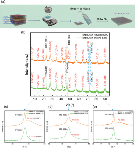
The initial step in this study involved the growth of BNMO/CeO2/SAO multilayer stacks on a STO substrate to produce freestanding BNMO/CeO2 thin films. Details on the fabrication process and additional technical specifics are detailed in our prior work.[21] Following a preparation process detailed in the experimental section and illustrated in Figure 1a, the STO substrate was efficiently recycled, subsequently depositing BNMO films on both pristine and recycled STO substrates for comparative analysis. The BNMO films grown on the two types of STO substrates were examined using XRD 2θ-ω scans, as presented in Figure 1b. The BNMO LSC (00l) peaks displayed a high degree of similarity in peak quality across both recycled and pristine STO substrates, suggesting an essentially identical crystalline structure within the LSC phase. Despite the close resemblance of the LSC peaks, a closer inspection around the STO peaks reveals notably stronger accompanying peaks in the recycled STO sample compared to the pristine counterpart, as illustrated in Figure 1c–e. These peaks are typically associated with the pseudo-cubic (PC) transitional interlayer, where biaxial strain accumulates and is eventually relaxed through dislocations, facilitating the emergence of the LSC phase.[28, 29] The pronounced intensity of PC peaks in the recycled STO sample indicates a significantly increased presence of the PC phase relative to the pristine sample. Notably, there is an evident shift in the PC peaks between the two samples. Specifically, the PC (001) peak in the recycled STO exhibits a 2θ value of 22.99°, compared to a 2θ value of 22.96° in the pristine STO, resulting in a shift of 0.03°. Quantitative analysis, based on Bragg's law (2dsin(θ) = λ), reveals the (001) d-spacing of the PC phase to be 3.866 Å in the recycled STO and 3.870 Å in the pristine STO. These results show great consistency with the lattice parameter measurement results detailed in Figure 2a2,b2, and the strain tensor mapping images in Figure 3a2,b2. Despite its subtle difference in the lattice parameter, this variation is significant as it mirrors changes in the surface characteristics of STO substrates from pristine to recycled conditions. Regarding the peaks annotated by the asterisk sign in Figure 1b, they denote minor impurity phases commonly observed in LSC thin films. These impurities, which may include bismuth oxide or transition metal oxides, are present in very minor quantities and do not impact the overall growth and properties of the thin films.
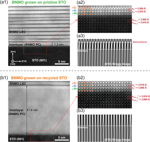
The interface microstructure of BNMO films grown on both pristine and recycled STO substrates was characterized using high-resolution STEM. In both cases, three distinct layers are identifiable: the substrate, a PC BNMO interlayer, and the BNMO LSC films. However, significant differences in microstructure between the samples were observed, as illustrated in the HAADF STEM images in Figure 2. For the pristine STO sample, the PC BNMO interlayer exhibits a thickness of ≈1.3 nm as shown in Figure 2a1, comprising four atomic layers. The minor variation in contrast between the topmost and middle layers of the BNMO film could be attributed to the slight variation in the TEM foil orientation or the film grain orientation through film thickness. Such grain orientation can occur in epitaxial thin film samples where, despite the substrate being perfectly aligned, the thin film itself may slightly deviate from the ideal zone axis alignment due to the growth dynamics and strain effects within the film layers. The transition to the LSC phase, facilitated by strain relaxation through edge dislocations, is depicted in Figure 2a2 and the corresponding (010) Bragg filtered image in Figure 2a3. In contrast, the PC BNMO interlayer in the recycled STO sample expands dramatically to 17.6 nm as shown in Figure 2b1, over an order of magnitude thicker than in the pristine counterpart. This discrepancy is also mirrored in the magnetic properties of the two samples; as Figure S1 (Supporting Information) reveals, BNMO films on recycled STO display weaker saturation magnetization and magnetic anisotropy than those on pristine STO, likely due to the augmented presence of the non-magnetic PC BNMO phase in the recycled sample. The thickness of the PC phase depends on its internal strain. Therefore, the increase in thickness suggests that the lattice mismatch between the PC phase and the recycled STO substrate has changed. Consequently, this suggests alterations in surface lattice structures of the STO substrate following the recycling process. Subsequent measurements of the lattice parameters of the PC phase and the STO atomic layers near the interface support this inference as displayed in Figure 2a2,b2. The c-axis parameter of the PC phase in both samples corresponds with the values calculated from XRD results. Nonetheless, the surface lattice parameters of the two STO substrates exhibit differences. Compared to the standard bulk STO lattice constants (a = c = 3.905 Å), the surface lattice of the pristine sample contracts to a = 3.900 Å and expands to c = 3.915 Å, whereas the lattice of the recycled sample stretches to a = 3.915 Å and contracts to c = 3.885 Å. This variation indicates that the surface lattice of the substrate experiences compression in the pristine sample and tension in the recycled sample, resulting in a different strain state of the PC phase. Consequently, the critical thickness required for the relaxation of biaxial strain in the PC phase also changes. Such phenomenon was consistently replicated in another recycled STO substrate, displaying an interlayer thickness of 16 nm as shown in Figure S2a (Supporting Information). To examine the possibility of thermal effects on the STO substrate, a pristine STO substrate was subjected to the same annealing conditions as that used for the SAO/CeO2/BNMO growth, and then used for BNMO deposition. Despite this annealing procedure, the thickness of the interlayer remained comparable to that observed in untreated pristine STO, as illustrated in Figure S2b (Supporting Information). These findings all suggest that the altered strain state of the recycled STO is mainly attributed to the influence of the SAO layer. This explains the distinct behavior of BNMO films grown on recycled STO compared to those on pristine STO. Prior to the deposition of BNMO films, the pristine STO presents an unstrained surface lattice, while the recycled STO exhibits a pre-strained surface lattice from the SAO layer growth. Consequently, the PC phase experiences varying degrees of lattice mismatch with the two substrates, resulting in differences in the strain state and the thickness.
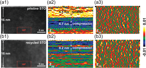
The modifications in strain states are further evidenced by GPA strain mapping images, as presented in Figure 3. GPA is an exceptionally powerful tool for microanalysis, offering a spatial resolution as fine as 1 pm, making it ideal for detecting changes on a very small scale.[36, 37] This analysis characterizes the surface lattice of both STO samples to a depth of ≈16 nm, offering a comparative view of their strain states. The analysis employs the bottom region as the reference zone (outlined by a red box) for GPA strain, which is relative to this reference zone, different from traditional strain measurements that are absolute and compared against the bulk lattice parameter. Notably, a distinct variation between the pristine and recycled STO samples is observed when comparing the strain tensor images along the y-axis in Figure 3a2,b2. Specifically, within ≈6.5 nm from the surface, the lattice of the pristine STO sample is elongated along the y-axis, while the lattice of the recycled STO sample exhibits compression along the y-axis within ≈8.2 nm from the surface. The compression region of 8.2 nm within the recycled STO primarily indicates an overall compression; however, the appearance of thin green or red areas, which suggest minor variation between tension and compression. This minor variation in strain state is due to the noise fluctuations inherent in high-resolution strain mapping measurements. These findings align with the lattice measurements depicted in Figure 2. Intriguingly, beneath the tension region in the pristine STO, there exists a compression region ≈6.7 nm thick, the origin of which remains unclear. One plausible explanation could involve the relaxation processes associated with the epitaxial strain from the overlying film layers. Even in pristine substrates, the growth of epitaxial layers can induce strain due to lattice mismatch or thermal expansion coefficient differences between the substrate and the film. As the film grows, this strain must be accommodated, potentially resulting in compressive stress in certain regions of the substrate. Additionally, mechanical stress can be introduced during the substrate handling before and during the deposition processes. These stresses may not be uniformly distributed, leading to localized compression and tension areas. Figure 3a3,b3 showcase the strain field images in the x-axis, where the strain field appears uniform across both samples. This uniformity is ascribed to the relatively minor strain along the x-axis compared to the y-axis, indicating changes in the a-axis are not discernible via GPA. The minimal strain observed along the x-axis can be attributed to the isochoric deformation, i.e., biaxial strain within the surface plane occurs in a square root manner, contrasting with the linear changes along the y-axis.
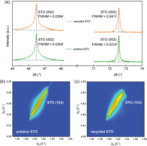
Having characterized the microstructure of BNMO films grown on different STO substrates, it is also important to investigate the lattice change in the plain recycled STO substrate compared to the pristine STO substrate. As previously mentioned, atomic layers near the surface of the recycled STO substrate may remain in a pre-strain state due to the SAO layer, potentially causing deviations from the ideal lattice arrangement. Figure 4a reveals that the 2θ-ω scans for the (002) and (003) peaks of recycled and pristine STO substrates exhibit notable differences in full width at half maximum (FWHM). Specifically, the FWHM for the (002) peak of recycled STO is 0.0384°, compared to 0.0304° for pristine STO, marking a difference of 0.008°. Similarly, for the (003) peak, recycled STO's FWHM is 0.0411°, versus 0.0310° for pristine STO, a difference of 0.0101°. Peak broadening in XRD analyses typically results from three primary factors: instrumental broadening, grain-size broadening, and micro-strain broadening.[38-40] Given the consistent use of the same optics setup for our measurements and the single-crystalline nature of the STO substrates, we can eliminate instrumental and grain-size broadening from our analysis. This leaves micro-strain broadening as the sole contributing factor. Strain within the diffracting crystals can cause shifts to higher or lower 2θ values, leading to overall peak broadening. In this instance, the near-surface atomic layers of the recycled STO substrate, affected by the SAO layer, exhibit broader XRD peaks than those of the pristine STO, indicating the presence of micro-strain. This is further supported by reciprocal space mapping (RSM) around the STO (103) peak for both pristine and recycled STO, as illustrated in Figure 4b,c. The RSM of the recycled STO (103) peak shows more pronounced broadening compared to the pristine STO, indicating a higher mosaicity and reflecting greater misorientation of crystalline domains within the material. This peak broadening serves as evidence of the increased variations in the strain states of the recycled STO.
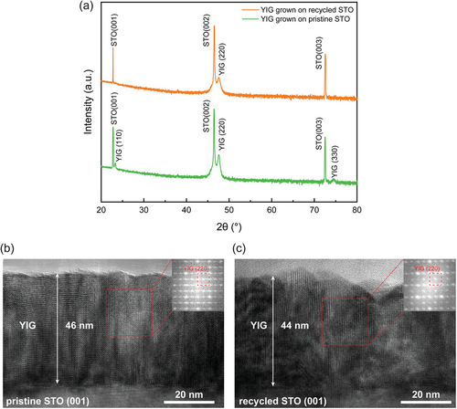
Based on the previous discussions, it is evident that recycled STO substrates differ from pristine STO substrates in the strain state on the surface, causing variations in the microstructure and properties of films grown on these substrates. This has been exemplified by BNMO films, which exhibit differing interlayer thicknesses and magnetic properties when grown on recycled versus pristine STO. To further investigate the impact of recycled STO substrates, a highly lattice mismatched YIG film was selected for this comparison study. The YIG films were grown on both types of STO substrates under identical growth conditions. YIG film is a ferrimagnetic material renowned for its outstanding magnon properties with low Gilbert damping coefficient and high thermal stability.[41-44] It is employed across a variety of technological fields including microwave, acoustic, optical, and magneto-optical applications.[41, 45-48] As illustrated in Figure 5a, YIG films exhibit markedly different peak qualities on recycled STO compared to pristine STO. While both display a YIG (110) | STO (001) epitaxial relationship, the peak intensity of the orthorhombic YIG on recycled STO is significantly weaker than on pristine STO, resulting in nearly invisible (110) and (330) peaks in comparison to those observed in the pristine STO case. Additionally, TEM analysis of the YIG films has revealed noticeable differences in morphology; although the films maintain similar thicknesses on both substrates, the film on recycled STO is less uniform than that on the pristine substrate as shown in Figure 5b,c. Localized fast Fourier transform (FFT) images show similar patterns between the two samples, yet the intensity of the diffraction spots varied, indicating differences in the crystallinity of the films. The chemical compositions of the films were also characterized using EDS mapping, as shown in Figure S3 (Supporting Information), which confirmed the uniform distribution of elements within the films, indicating a good growth quality of the YIG film on both substrates.
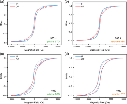
To investigate the magnetic properties of YIG films, magnetization-field (M-H) measurements were conducted using the VSM mode of MPMS3 at room temperature (300 K) and low temperature (10 K), with the 10 K data being collected post a field cooling with no magnetic field applied. The M-H curves were measured in both in-plane (IP) and out-of-plane (OP) directions with a magnetic field of up to 10,000 Oe. These results are plotted in Figure 6 and tabulated in detail in Table S1 (Supporting Information). At both temperatures, typical magnetic hysteresis loops are observed for the two samples. Upon comparing the values documented in Table S1 (Supporting Information), a distinct difference in coercive field (Hc) is observed. Notably, at 300 K, the OP direction shows a lower coercive field (Hc) in the pristine STO sample, while the IP direction has a lower Hc in the recycled STO, indicating a shift in preferred magnetic anisotropy from OP in the pristine to IP in the recycled STO. To numerically express this magnetic anisotropy, the difference in Hc values is computed using the formula ΔHc = (Hc, OP − Hc, IP)/Hc, OP. The resultant ΔHc values for the pristine STO sample and recycled STO sample are -18.90% and 40.89%, respectively. At 10 K, Hc increases significantly as shown in Figure 6c,d, and the easy axis orientation remained unchanged in both samples. Additionally, the change in ΔHc values to −42.29% for the pristine STO and 6.65% for the recycled STO indicates that the pristine STO sample exhibits stronger magnetic anisotropy at the lower temperature of 10 K compared to 300 K, while the recycled STO sample shows weaker magnetic anisotropy at the lower temperature. This behavior in the pristine STO aligns with the conventional theory that magnetic anisotropy decreases as temperature increases, showing a negative temperature coefficient;[49, 50] however, the behavior in the recycled STO does not follow this trend.[51] Such variations in magnetic behavior could be attributed to differences in film crystallinity between the two samples. Concerning the magnetic anisotropy in YIG thin films, we hypothesize that the variation in magnetic anisotropy between the films grown on recycled substrates versus pristine substrates can be attributed to several factors directly related to the substrate's pre-strain condition. First, the pre-strain in the recycled STO substrates may lead to slightly altered lattice parameters in the YIG films grown on these substrates. This distortion can change the symmetry of the magnetic ion environments, thereby influencing the magnetic anisotropy. The strain transfer from the substrate to the film could result in different magnetoelastic contributions, which directly affect the magnetic anisotropy. Second, the different surface conditions of the recycled versus pristine substrates may lead to variations in the growth dynamics of the YIG films. These variations can influence film thickness, interface roughness, and defect densities, which could also impact magnetic properties. Hence, YIG films grown on the pristine and the recycled STO substrates exhibit distinct crystallinity and magnetic properties, highlighting the need for careful consideration when reusing recycled STO substrates for thin film growth. We've also conducted preliminary ferromagnetic resonance (FMR) measurements on the YIG films grown on both pristine and recycled STO substrates. However, no obvious FMR response was observed in either case. This result might be attributed to the crystalline structure of the YIG films used in our experiments, which were in the orthorhombic phase. Historically, FMR responses have been predominantly reported and observed in cubic phases of YIG grown on gadolinium gallium garnet (GGG) substrates.
All of these findings suggest that it is feasible to reuse the recycled STO and perhaps many other oxide substrates, except MgO, which presents a water hydration process. Exploring similar surface modification effects on substrates such as Si or LaAlO3 (LAO) would be a valuable extension of this research. While the modification effects might be less pronounced on these substrates compared to STO, due to their different material properties and responses to strain, the potential for sustainable processing and cost reduction remains significant. For instance, Si substrates are widely used in semiconductor industry, and integrating complex oxide thin films onto Si through a recyclable process could lead to more efficient manufacturing practices and broader applications.[56, 57] It could be beneficial to grow highly mismatched films on recycled substrates considering its improved critical thickness in PC BNMO interlayer and ease in accommodating large mismatch. On the other hand, a careful comparison between the different cycles of the recycling and redeposition process is necessary for reproducible film quality prepared by the recycling process. All of these studies suggest it is practical to reuse the substrates after SAO water dissolution process and thus could be a sustainable approach for complex oxide process in semiconductor manufacturing process.
3 Conclusion
In conclusion, this study elucidates the impact of water dissolution and recycling on STO substrates and its effects on the growth and properties of the subsequently grown BNMO and YIG films. The introduction of a pre-strain state in the recycled STO by the SAO layer leads to notable differences in the microstructure and properties of subsequently grown films on recycled versus pristine substrates. Obviously increased PC BNMO interlayer thickness in LSC films and the growth of large mismatched YIG films on recycled STO substrates all suggest that there are obvious changes in the recycled substrates. Specifically, there are distinct changes in lattice parameters and strain states, as indicated by XRD and RSM minor peak broadening. High-resolution TEM/STEM analysis and GPA strain mapping further validate these findings, showing altered strain in the recycled STO and modified microstructure in the films. The impact of substrate alterations is further illustrated by the differences observed in the crystallinity and magnetic properties of YIG films grown on recycled STO compared to those grown on pristine STO. The uniformity in Raman spectra and chemical composition, as assessed by XPS, does not fully capture the underlying alterations in the lattice structure and strain, which are critical to the properties of the films grown. These subtle differences, particularly in terms of mechanical properties such as Young's modulus, underscore the potential mechanical property changes on the STO surface. Moving forward, further research should explore the comprehensive effects of recycling on substrate integrity and film quality, and the impacts from multiple recycling steps if this is adopted by semiconductor industry. These recycled substrates could revolutionize the production of complex oxide thin films, which are essential components in the manufacture of advanced electronic devices, including sensors, transistors, and capacitors. By enabling the reuse of substrates, our research promotes cost reduction and increases manufacturing efficiency, which are crucial for scaling up production and enhancing the sustainability of the electronics and photonics industry. The recycled substrates could be directly used to grow highly lattice mismatched films with enhanced film quality and properties. For more consistent reproducibility of redeposition in semiconductor industry, an acid etching step might be needed for substrate surface treatment after recycling. This work not only advances our understanding of surface modification introduced by substrate recycling process but also provides initial demonstration for cost-effective and sustainable growth process of functional oxides via recycled substrates.
4 Experimental Section
Thin Film Growth
All the films were grown on either pristine or recycled STO (001) substrates by pulsed laser deposition (with a KrF excimer laser, Lambda-Physik COMPex Pro 205, λ = 248 nm). A detailed growth recipe of SAO/CeO2/BNMO multilayer films can be found somewhere else.[21] The BNMO film was deposited on two kinds of STO substrates at a temperature of 600 ̊C and an oxygen pressure of 200 mTorr, utilizing a laser fluence of 3.6 J cm−2 and a pulse repetition rate of 2 Hz. Following the deposition process, the films underwent an annealing procedure at 400 ̊C under an oxygen pressure of 500 Torr for a duration of 1 h. The cooling phase to room temperature was carried out at a rate of 10 ̊C min−1. The YIG film was deposited on two kinds of STO substrates at a temperature of 850 ̊C and an oxygen pressure of 50 mTorr, utilizing a laser fluence of 3.2 J cm−2 and a pulse repetition rate of 5 Hz. After the deposition, the films were subjected to an annealing process at 850 ̊C in an oxygen atmosphere at 50 mTorr pressure for an hour. They were then cooled to room temperature at a controlled rate of 15 ̊C min−1.
Preparation of Recycled STO Substrates
After the growth of SAO/CeO2/BNMO multilayer thin films, the STO substrates were submerged with the deposited layers in a heated ultrapure water bath to dissolve the SAO layer gently. This process typically takes place at ≈80 °C. Once the SAO layer was completely dissolved, the substrates were removed from the bath. Then, the substrates were rinsed and sonicated in ultrapure water to wash away any remaining residues. Finally, the substrates were dried using a gentle stream of nitrogen to ensure that the surface was free of any organic or inorganic residues.
Sample Characterization
Various methods were employed to examine the microstructure and crystallinity of the samples. XRD analyses were carried out using a PANalytical Empyrean instrument. For transmission electron microscopy (TEM) and high-angle annular dark-field (HAADF) STEM, a Thermo Fisher Scientific TALOS 200X, operating at 200 kV, was utilized. Additionally, a FEI Titan™ G2 80–200 STEM equipped with a Cs probe corrector and ChemiSTEM™ technology, including X-FEG™ and SuperX™ energy-dispersive X-ray spectroscopy (EDS) with four windowless silicon drift detectors, was operated at 200 kV for further analysis. Sample preparation for STEM observation involved manual grinding, thinning, dimpling, and ion milling with a precision ion polishing system (PIPS II Model 695, Gatan). The chemical composition of the thin films was explored using the EDS mode in STEM. For GPA, a Digital Micrograph plugin (DM 3.5 package, HRTEM Research Inc.) was employed.
Raman spectroscopy measurements were conducted using a Renishaw inVia Raman microscope, operating at a 532 nm wavelength. The surface topology of the samples was investigated using a Bruker Dimension Icon AFM. XPS analysis was carried out with a Kratos Axis Supra XPS system, equipped with a monochromatic Al Kα X-ray source. Each sample's surface underwent an initial XPS scan before executing a depth profiling analysis through 40 steps, utilizing a gas cluster ion sputtering system. This system operated at 10 keV with 1000 clusters for a 60 s duration, at an incidence angle of 40 degrees relative to the horizontal plane. The analysis covered an area of 110 µm by 110 µm, with a sputtering size of 2 mm by 2 mm. The base pressure during the XPS analysis was maintained at 1.2 × 10⁻⁹ torr, and the electron emission angle was set at 54.7°, with an active charge neutralizer in use. Data from the XPS were processed using CasaXPS software. For calibration of peak positions across all samples, the C 1s signal at 284.8 eV served as the internal reference.
Magnetic Properties Measurements
The magnetic characteristics of the samples were examined using the vibrating sample magnetometer (VSM) functionality of the Magnetic Property Measurement System (MPMS3 by Quantum Design). Magnetization versus magnetic field curves were recorded for both the in-plane and out-of-plane orientations. To ensure the accuracy of the results, initial calibration errors were addressed. Corrections for the high-field slope and magnetic remanence were made using a correction script from the instrument's software. The effects of the sample shape on the measurements were also considered. The correction factor for this, which ranges from 0.9 to 1.2, was determined using the instrument's sample geometry calculation tool.
Mechanical Properties Measurements
Hardness and modulus of both STO substrates were measured on a Hysitron TI Premier nanoindenter using the displacement control mode. At least 100 indents were conducted on each sample to ensure the data reliability.
Acknowledgements
This work is funded by the U.S. National Science Foundation (DMREF-2323752). Z.H. and M.M. acknowledge the support from the U.S. Department of Energy (DE-SC0020077) for property testing. The high-resolution STEM imaging work was funded by the U.S. National Science Foundation (DMR-2016453) and the Laboratory Directed Research and Development program at Sandia National Laboratory. X.S. acknowledges the support from the DoE-BES (Basic Energy Sciences) under grant no. DE-SC0016337. L.Q., J. B., P.L., and J.D. acknowledge the support from the Laboratory Directed Research and Development program at Sandia National Laboratories, a multi-mission laboratory managed and operated by National Technology and Engineering Solutions of Sandia, LLC, a wholly owned subsidiary of Honeywell International, Inc. The article describes objective technical results and analysis. Any subjective views or opinions that might be expressed in the article do not necessarily represent the views of the U.S. Department of Energy or the United States Government.
Conflict of Interest
The authors declare no conflict of interest.
Author Contributions
The idea for this research project was conceived by J.S. and H.W. They collectively designed all the experiments and developed the mechanistic understanding behind the study. J.S. took charge of the TEM/STEM/EDS, GPA analysis, XRD, and AFM characterization work. Also, J.S. conducted the data analysis and visualization work. L.Q. helped grow YIG films on the two STO substrates and collect the magnetic data. J.B. helped collect the RSM data of the two samples. B.T. was responsible for creating the conceptual drawings and Raman measurement. The high-resolution STEM characterization work was helped by P.L. and J.D. The XPS data was collected by D.Z. and analyzed by Y.Z. The mechanical test was performed by X.S. and C.S. The TEM sample preparation work was finished by J.G., M.M., Z.H., and J.H. The experimental funding for the project was acquired by H.W. The manuscript was mainly written by J.S. with suggestions from H.W. All authors have reviewed and approved the final version of the manuscript.
Open Research
Data Availability Statement
The data that support the findings of this study are available in the supplementary material of this article.


