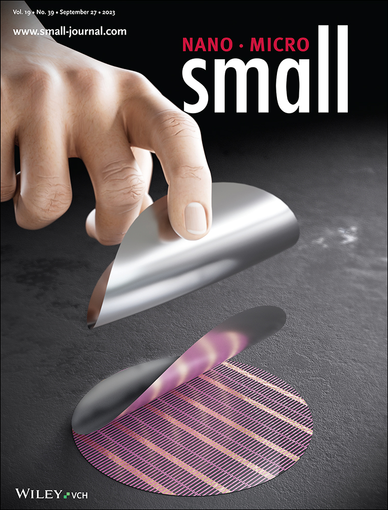
Large-Area Synthesis of Ferromagnetic Fe5−xGeTe2/Graphene van der Waals Heterostructures with Curie Temperature above Room Temperature
Abstract
Van der Waals (vdW) heterostructures combining layered ferromagnets and other 2D crystals are promising building blocks for the realization of ultracompact devices with integrated magnetic, electronic, and optical functionalities. Their implementation in various technologies depends strongly on the development of a bottom-up scalable synthesis approach allowing for realizing highly uniform heterostructures with well-defined interfaces between different 2D-layered materials. It is also required that each material component of the heterostructure remains functional, which ideally includes ferromagnetic order above room temperature for 2D ferromagnets. Here, it is demonstrated that the large-area growth of Fe5−xGeTe2/graphene heterostructures is achieved by vdW epitaxy of Fe5−xGeTe2 on epitaxial graphene. Structural characterization confirms the realization of a continuous vdW heterostructure film with a sharp interface between Fe5−xGeTe2 and graphene. Magnetic and transport studies reveal that the ferromagnetic order persists well above 300 K with a perpendicular magnetic anisotropy. In addition, epitaxial graphene on SiC(0001) continues to exhibit a high electronic quality. These results represent an important advance beyond nonscalable flake exfoliation and stacking methods, thus marking a crucial step toward the implementation of ferromagnetic 2D materials in practical applications.
1 Introduction
2D ferromagnetic materials are anticipated to play a crucial role in the development of future spin-based devices (e.g., spin-valves and random-access magnetic memories) with high energy efficiency and ultracompact dimensions.[1-3] Moreover, combining them with other layered materials such as graphene and 2D semiconductors (e.g., WS2 and MoSe2) into van der Waals (vdW) heterostructures is a promising pathway for the realization of novel devices with integrated magnetic, optical, and electronic functionalities.[4] In this case, besides the individual properties of each 2D crystal, proximity-induced coupling effects across the vdW gap offer unique opportunities to tailor properties via a layering design.[4, 5]
In order to enable a broad range of applications, it is critical to identify 2D ferromagnets exhibiting a Curie temperature (TC) at least at room temperature.[2, 6] Among a vast selection of 2D materials with magnetic order investigated recently,[6] the Fe5−xGeTe2 (FGT) metallic system (with x usually between 0 and 0.4)[7-10] has been found to offer a great prospect, as it has been reported to exhibit a TC of around 300 K.[7, 10, 11] FGT is an itinerant ferromagnetic metal[11] with magnetic properties that can be tuned via electrostatic gating,[12] strain, or doping when interfacing a topological insulator,[13] as well as elemental doping.[14, 15] Similar to other 2D Fe–Ge–Te compounds like Fe3GeTe2[16] and Fe4GeTe2[17] with below room temperature TC, it possesses a layered structure with each single layer being formed of Fe and Ge 2D slabs encapsulated by layers of Te.[7, 8] The weak vdW interaction between interlayers permits to exfoliate micrometer-sized flakes from FGT bulk single crystals and to fabricate vdW heterostructures combining FGT and other 2D crystals via sequential flake stacking.[18-20] Such an approach has recently been used to realize FGT/graphene spin-valve devices demonstrating room-temperature operation.[18] FGT/graphene vdW heterostructures are in general very promising for the design of all-2D logic/multiplexer devices[4] in which FGT is the spin injector/detector and graphene the spin-transport channel.
Despite their great utility for fundamental studies and testing device concepts, exfoliation-based methods are not scalable and difficult to integrate into established device fabrication schemes. Hence, achieving bottom-up synthesis of 2D heterostructures comprising FGT and graphene is crucial for implementing these materials into future devices. In this work, we demonstrate the synthesis of large-area FGT/graphene vdW heterostructures exhibiting ferromagnetic order persisting well above 300 K and perpendicular magnetic anisotropy (PMA). For this, vdW epitaxy of FGT films on single-crystalline graphene/SiC(0001) templates was realized by molecular beam epitaxy (MBE), a method which has recently been employed for the growth of FGT on substrates such as Al2O3(0001), WS2(001)/Al2O3(0001), and SrTiO3(111).[9, 13, 21] Importantly, the underlying graphene layers exhibit a sharp interface to the FGT and conserve their high electronic quality, which are key ingredients for the future development of devices in which interfacial effects can be used to control properties and functionalities.
2 Results and Discussion
2.1 Structural Properties
MBE was employed to grow ≈15 nm thick FGT films on epitaxial graphene on SiC (0001) templates synthesized by surface graphitization.[22] Rutherford backscattering spectrometry (RBS) analyses (see Figure S1 in the Supporting Information) revealed the films to exhibit an average composition close to x = 0, namely Fe4.8GeTe2. This is similar to what has been reported for bulk single crystals synthesized by chemical vapor transport.[7, 23] In situ growth monitoring by reflection high-energy electron diffraction (RHEED) showed a pattern composed of isolated streaks which indicates growth of a film with a smooth surface (Figure 1a, bottom panel). The position of the streaks with respect to the pattern measured for epitaxial graphene on SiC(0001) before growth (for SiC(0001), the in-plane (IP) lattice parameter is 3.08 Å)[24] attested the evolution to a larger in-plane lattice constant around 4.06 Å, as expected for FGT formation.[9]

To study the in-plane structure in more detail, synchrotron-based grazing incidence diffraction (GID) was employed. Figure 1b shows the in-plane intensity distribution plotted in hexagonal coordinates according to the symmetry of the SiC(0001) substrate. This map was obtained for the 15 nm FGT film covered by a 5 nm thick Te capping layer, which was used to reduce FGT surface oxidation upon prolonged air exposure. For convenience, we use the four-component vector notation for hexagonal symmetry: (H K. L) = (H K −[H + K] L). The only substrate contribution within the investigated area in reciprocal space appears as a single (2.0)-type reflection. The other most intense and prominent diffraction features originate from the FGT film. There are two different sets of reflections, namely FGT(11.0) and (22.0), and FGT(H0.0) with [H = 1,…,3]. They both refer to orientations with their c-axes along the surface normal. The three most intense diffraction features at (11.0), (22.0), and (30.0) reveal an FGT in-plane lattice parameter of 4.049(13) Å. This is, in general, agreement with the value obtained by RHEED, as well as literature values for Fe5−xGeTe2 (0 < x ≤ 0.4) bulk crystals[7, 8, 10] and thin films.[9, 13]
The intensity modulation along the FGT(11.0) ring exhibits a maximum in the azimuth which is aligned along the SiC[2.0] in-plane substrate direction. This indicates a preferential in-plane orientation, i.e., the (11.0) net planes of FGT and SiC are parallel, as we previously observed for Fe3GeTe2 films grown on graphene.[25] Nevertheless, the FGT arc maxima are broader than those of Fe3GeTe2. For the arc crossing the (11.0) reflection, a full width at half maximum of 8.9° (Figure 1b, inset) is found, whereas for Fe3GeTe2 this value is about 4.7°.[25] Even though this relatively large value is not uncommon for epitaxially grown vdW materials,[26-28] it reveals that the in-plane mosaicity in the FGT film is clearly larger than that measured for the Fe3GeTe2 one (grown with virtually identical conditions, except the Fe flux). This difference might be associated with the higher energies required for the stabilization of layered Fe–Ge–Te phases exhibiting a Fe composition higher than 3.[17] The existence of in-plane mosaicity can also be inferred from the rather diffuse streaks of the RHEED pattern (Figure 1a, bottom panel). Similar RHEED patterns were reported by Ribeiro et al.[9] for Fe5GeTe2 films grown by MBE on Al2O3(0001) substrates. Interestingly, they could observe an evolution from diffuse to sharp RHEED streaks by performing postgrowth annealing of the films at a temperature of 550 °C under Te flux. This suggests that postgrowth thermal treatment as well as higher growth temperatures might improve in-plane order for FGT films grown on graphene. This will be the topic of further investigations. There are two more ring-like contributions detectable in the map and in the attached line profile taken at K = 0, which cannot be related to FGT. These are most probably due to a smaller fraction of tetragonal FeTe agreeing very well with FeTe(200) and (220) in-plane lattice spacing. Interestingly, the c-axis of tetragonal FeTe points along the direction perpendicular to the surface as well. Finally, a sequence of low-index polyrings with different lattice spacings is also detected, which is originating from the topmost Te capping layer.
Complementary to GID we have performed a laboratory-based omega/2theta measurement at an X-ray wavelength of 1.54056 Å, which probes exclusively out-of-plane features of the layer (see Figure 1c). A set of FeTe reflections confirms the presence of tetragonal FeTe with its out-of-plane orientation along SiC [00.1] as it could already be anticipated from the GID in-plane data. A further set of eight subsequent FGT(00.L) reflections with L = 3, 6, …, 24 proves (in conjunction with the presented in-plane data) the formation of FGT with a Fe5GeTe2 structure,[8] since they fit well to the position and intensity ratios of the numerically derived powder pattern (black bars). Based on the positions of the contributions at L = 3, 6, 18, and 21, we have deduced an out-of-plane lattice parameter of 29.16(9) Å, in agreement with previous reports for bulk crystals and thin films.[7-10, 13] The formation of [00.1]-oriented Fe3GeTe2 can be excluded as it would result into a clearly different diffraction pattern.[16, 29] Note that these measurements were performed for uncapped FGT films, which explain the absence of contributions related to pure Te.
The surface morphology was probed by atomic force microscopy (AFM). Figure 1d shows a typical AFM height image for an uncapped FGT film. Its coverage appears mainly continuous over the micrometer-sized graphene/SiC terraces, with the exception of some holes appearing close to surface steps. These substrate regions are known to exhibit few-layer thick graphene ribbons and patches, whereas the terraces are mostly covered in monolayer—and, to a lesser extent, bilayer—thick graphene.[28, 30] A similar effect was observed in Fe3GeTe2 grown on graphene/SiC(0001),[25] which we associated with the lower surface reactivity of the thicker graphene areas relative to that of the terraces,[22] leading to a lower FGT growth rate near the steps. Moreover, it is possible to observe nanoislands with tetragonal shapes scattered over the surface (Figure 1d, inset). Based on the GID and X-ray diffraction (XRD) findings, we suggest that they are composed of tetragonal FeTe,[31] forming due to phase segregation during growth or during subsequent sample cooling. In spite of these unwanted surface effects—which are expected to be mitigated by further refinement of both the FGT and graphene growth protocols—it is reasonable to conclude that the FGT film offers a good surface homogeneity over large areas. The root-mean-square (RMS) roughness for different surface regions (free of FeTe nanoislands) varies between 0.8 and 1.1 nm, which is close to the thickness of one monolayer of Fe5GeTe2 (a single layer corresponds to 1/3 of the unit cell with c = 29.16(9) Å). It is important to note that the AFM investigations discussed here were conducted on noncapped FGT films. Although oxidation in FGT[32] is not as strong as in 2D magnetic halides,[33] surface oxidation taking place within a few hours after air exposure might increase the surface roughness.
The structure of the FGT/graphene heterostructure was also investigated by scanning transmission electron microscopy (STEM). Figure 2a depicts a high-angle annular dark-field (HAADF)-STEM image of the FGT film grown on graphene/SiC(0001). It is possible to observe the layered structure of the film; in that single layers are clearly separated by vdW gaps, in agreement with previous TEM characterization of FGT bulk crystals and thin films.[7, 9] Most of the film is formed of well-oriented layers with the expected FGT single-layer thickness (≈1 nm, see Figure 2b). This value agrees with the c lattice constant obtained from the XRD data. Stacking and rotational faults are also evident. Strikingly, STEM images reveal that, although the overall vdW-layered structure is preserved, single layers with a thickness larger than 1 nm are also present. Figure 2c, which shows an enlarged area from an interface region in Figure 2a, reveals some layers as thick as 2 nm. To the best of our knowledge, the experimental realization of Fe–Ge–Te-layered phases in which the thickness of a single layer is larger than that of Fe5GeTe2 has not been reported. In a simple picture, such a thickness increment is anticipated if one considers that “filling” the 2D backbone structure of Fe5GeTe2 with more Fe atoms will result in the formation of additional slabs of Fe, following the same trend as experimentally observed when transitioning from Fe3GeTe2 to Fe5GeTe2 (for which the single-layer thickness evolves from ≈0.8 to ≈1.0 nm).[7, 8, 16, 34] In fact, Liu et al.[35] used first-principles calculations to study different Fe–Ge–Te-layered phases including Fe6GeTe2 and Fe7GeTe2. They predicted them to exhibit a thickness for single layers of around 1.1 and 1.2 nm, respectively. Our XRD data (Figure 1c) do not directly confirm the formation of such phases, which shows that they are not dominant in the film. However, the shift of the (00.9) reflection toward a lower angle (in comparison to the value calculated for Fe5GeTe2), as well as the existence of an additional, unidentified reflection closed to (00.18) (superimposed to SiC (00.6)), could be related to the existence of layered phases with larger c lattice constants.
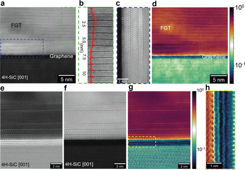
Even though at the present stage we cannot unambiguously identify their composition and structure, the existence of single layers with thickness larger than that of Fe5GeTe2 is strong evidence for the formation of new Fe–Ge–Te-layered phases with Fe composition exceeding 5, which are possibly metastable.[17] This illustrates the great potential of vdW epitaxy via MBE for the large-scale realization of metastable phases of 2D magnets, similar to what have been observed for 2D semiconducting dichalcogenides.[36, 37] Further investigations are needed in order to identify the reasons for the formation of such phases and to controllably realize them. Finally, note that the average RBS composition obtained for our films (Fe4.8GeTe2) does not pose a contradiction to the existence of layers with higher Fe concentration. It is known that Fe5−xGeTe2 single layers are usually Fe-deficient with 0 < x ≤ 0.4[8, 10, 38, 39] (x can be even close to 1 if the Fe4GeTe2 structure stabilized by Seo et al.[17] is considered, which interestingly also exhibits a single-layer thickness of around 1 nm). Fe deficiency taking place in the “normal” FGT layers could, in principle, compensate for the higher amount of Fe present at the less abundant, thicker layers.
Another very important feature observed in the STEM images is the sharp nature of the FGT/graphene interface. Figure 2d depicts the same area as in Figure 2a, rendered using a custom color map to aid the visualization of the graphene layers, since the HAADF-STEM images provide an atomic number (Z) contrast. The continuous graphene layers are observed (dark green color) directly interfacing the crystalline FGT film (in orange). A more detailed view of the FGT/graphene interface, obtained for another sample region, is provided in Figure 2e–h. In agreement with the previous reports,[22] they confirm the existence of a bilayer thick graphene (with an interlayer distance of 0.34 nm), and the carbon-rich buffer layer very close to SiC.
2.2 Magnetic and Electric Properties
The magnetic and electric properties were investigated via magnetotransport measurements, superconducting quantum interference device (SQUID) magnetometry, X-ray absorption spectroscopy (XAS), and X-ray magnetic circular dichroism (XMCD). These measurements were performed on pieces cut from the same 1 cm2 sample consisting of an ≈15 nm FGT film (capped with 5 nm Te) grown on graphene/SiC(0001).
Figure 3a displays the Hall resistivity ρxy measured via magnetotransport during upward and downward sweeps of an external magnetic field H, where the arrows indicate the field sweeping directions. The linear background is caused by the ordinary Hall effect (OHE) with the negative slope observed for the whole temperature range suggesting electron-like transport behavior. However, the measured OHE results from parallel conduction through the FGT and graphene transport channels exhibiting hole- and electron-like transport characteristics, respectively.[25] Consequently, the sign as well as the absolute value of the OHE slope depend on the relative conductivities of the FGT and graphene films. The extracted effective carrier density of 1.0 × 1014 cm−2 and the sheet resistance of 176 Ω sq−1 (at room temperature) in our FGT/graphene heterostructure are close to the values obtained for the previously studied Fe3GeTe2/graphene heterostructure (7 × 1013 cm−2 and 150 Ω sq−1, respectively).[25] The observed hysteresis loop superimposed onto the OHE at each temperature originates from the anomalous Hall effect (AHE), its signal strength being proportional to the out-of-plane magnetization. The nearly square-shaped loops and the finite coercivity observed for temperatures up to 360 K provide clear evidence for ferromagnetism well above room temperature with a robust PMA. Similar results obtained for an ≈10 nm FGT film are shown in Figure S2 (Supporting Information). For the determination of the Curie temperature, we adopt the commonly used method based on the Arrott plot;[17, 40] ρA2 is plotted against µ0H/ρA, where ρA is the AHE part of the Hall resistivity after subtracting the linear background of the OHE contribution (see also Figure S3 in the Supporting Information). From the linear fit in the high-field ranges of the Arrott plots in Figure 3b, the intercepts at the ρA2 axis are extracted for each temperature. As shown in Figure 3c, these intercepts exhibit a linear temperature dependence in accordance with Arrott's theory.[40] Finally, a Curie temperature of TC ≈ 390 K is extracted from the extrapolation to zero intercept by a linear fit (red line in Figure 3c; see also Figure S2 in the Supporting Information). The same TC is obtained from the temperature decays of the remanent AHE resistivity and the coercive field (Figure S3, Supporting Information). This value is significantly higher than those previously reported for single crystals (or flakes) as well as large-area films of Fe3GeTe2 (TC ≈ 220 K),[25, 29, 41, 42] Fe4GeTe2 (TC ≈ 270 K),[17] and Fe5−xGeTe2 (0 < x ≤ 0.4, TC ≈ 280–320 K).[7, 9, 21, 39, 43] Only the transition temperature recently reported for MBE-grown Fe5−xGeTe2/Bi2Te3 heterostructures (TC as high as 570 K) surpasses this value.[13]
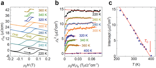
The high TC value approaching 400 K is in agreement with a recent theoretical prediction for the Fe5GeTe2 phase;[17] however, it differs from other experimental reports for Fe5−xGeTe2. This could be related to the existence of thicker single vdW FGT layers, as observed by STEM. It is anticipated that a gradual increase of the Fe content within individual layers will result in a larger number of nearest Fe neighbors per Fe atom, enhancing the spin–pair exchange interaction and consequently the Curie temperature. In fact, recent theoretical investigations predicted PMA and TC values of 450 and 570 K for layered Fe6GeTe2 and Fe7GeTe2, respectively.[35] Therefore, in the case of our samples, the existence of similar phases with Fe composition higher than 5 could, in principle, lead to an effective TC value that is superior to that of pure Fe5−xGeTe2. Nevertheless, in order to verify this hypothesis, future growth experiments will be conducted aiming at the stabilization, and isolation, of such phases. Finally, note that the tetragonal FeTe phase detected by GID and XRD (Figure 1b,c) and correlated to the surface nanoislands observed by AFM (Figure 1d) is not expected to contribute to the observed ferromagnetism due to its anti-ferromagnetic nature (Néel temperature of around 70 K).[31]
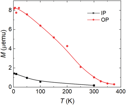
The magnetic properties of the FGT film were further investigated by SQUID magnetometry. Figure 4 displays the remanent magnetization obtained for both out-of-plane (OP) and in-plane (IP) configurations as a function of temperature (a background signal caused by the SiC substrate has been subtracted; Figure S4, Supporting Information). The clearly larger remanent magnetization in the OP configuration confirms the PMA in our FGT films. Furthermore, it is clear from the decay of the OP remanent magnetization that ferromagnetic order persists well above room temperature, in agreement with the result extracted from the AHE measurements. The Fe atoms on the five inequivalent lattice sites in Fe5GeTe2 are expected to exhibit rather different magnetic moments.[7, 38] The average magnetic moment per Fe atom obtained from the SQUID data measured at 2 K is 1.37 µB, considering the average Fe concentration of 4.8 as obtained by RBS measurements. This result falls into the range between 0.8 and 2.6 µB per Fe atom covered by reported experimental values.[7]
XAS and XMCD measurements were employed to investigate the atomic-scale magnetic properties.[44] Figure 5 shows the remanence of the dichroic signal at B = 0 T (normalized by its value at B = 6 T), for both grazing (20° from the sample plane) and normal incidence geometries, as a function of temperature. At low temperature, the sample has a PMA, as evidenced by the larger remanence in the perpendicular direction (red triangles). However, above T = 220 K, the measured magnetization undergoes an in-plane reorientation transition. The spontaneous magnetization persists above room temperature (Figures S6 and S7, Supporting Information).
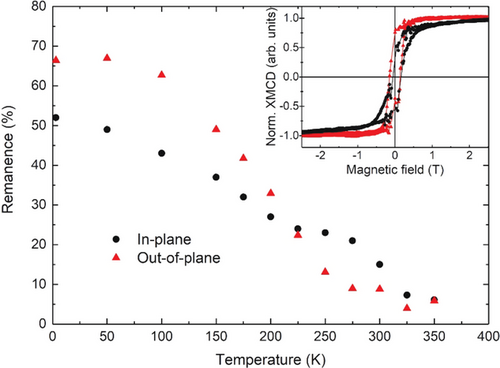
We performed a sum-rule analysis on the XAS–XMCD spectra at T = 3 K to extract the atomic magnetic moments of Fe atoms (Figure S5, Supporting Information). We obtained an effective total magnetic moment in normal incidence (i.e., not corrected from the intra-atomic dipole operator Tz) Meff = 1.13 ± 0.15 µB per Fe atom, in reasonable agreement with the value obtained by SQUID. The lower value found from this analysis might be due to the fact that not all Fe atoms probed in XAS contribute to the magnetic signal obtained by XMCD (e.g., those part of anti-ferromagnetic FeTe nanoislands do not contribute); thus, this value is an underestimation of the actual Fe magnetic moment in FGT. This analysis also allowed us to extract the orbital moments measured in normal incidence µB/Fe and the difference between perpendicular and in-plane orbital moments that is proportional to the macroscopic anisotropy in itinerant magnetism materials according to Bruno's model.[45] We found ΔmL < 0.01 µB, consistent with the small anisotropy observed in normal (red curve) and grazing (black curve) hysteresis loops shown in the inset of Figure 5.
A TC above room temperature, as observed in XMCD, is in good agreement with literature values for Fe5−xGeTe2 with x ranging from 0 to 0.3.[9, 10, 21, 39] Certain discrepancy observed between XMCD, SQUID, and magnetotransport results, in terms of remanence, anisotropy and TC may be attributed to the fact that the different experiments probe different parts of the FGT film. While SQUID probes the whole film, the detection in XMCD is restricted to the topmost FGT layers (≈5 nm). As observed by STEM (Figure 2a), this area is formed exclusively of single layers with the interlayer spacing expected for Fe5−xGeTe2 with x being close to 0. Also, the grazing geometry measured in XMCD does not correspond to a purely in-plane component of the magnetization, but instead it has a contribution from the out-of-plane one. For the magnetotransport (AHE) measurements, the actual current distribution between the different FGT components and the graphene film is essential but difficult to determine.
3 Conclusion
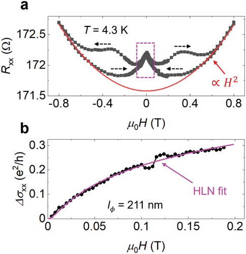
Our results demonstrate the successful growth of a large-area 2D heterostructure with high quality of the individual FGT and graphene components, as well as of the interface between them, which was previously achieved only by manually assembling flakes of the different materials. This constitutes a critical step toward the implementation of these materials in future technologies. Morphological and structural characterization revealed the fabrication of continuous heterostructure films with a sharp interface between FGT and graphene. Interestingly, stacking faults related to the presence of single vdW layers with thicknesses exceeding those expected for the Fe5GeTe2 phase are identified by STEM. We expect these to be FGT phases with Fe composition higher than 5 and potentially enhanced magnetic properties. Future investigations will be carried out to clarify this aspect. Different methods used to study the magnetic and transport properties revealed that the ferromagnetic order persists well above room temperature with perpendicular magnetic anisotropy. In addition, the underlying graphene film continues to show quantum features in its electronic properties, attesting to the conservation of its high quality after vdW epitaxy of FGT.
4 Experimental Section
Epitaxial Graphene on SiC
Semi-insulating 4H-SiC(0001) substrates with sizes of either 1.0 cm × 1.0 cm or 0.5 cm × 1.0 cm were chemically cleaned in n-butyl acetate, acetone, and propanol. After that, they were loaded in an induction-heated furnace pumped down to a base pressure of 10−4 mbar. In order to remove surface irregularities and create well-defined stepped surfaces, an H-etching treatment was performed at 1400 °C for 15 min in forming gas atmosphere (95% Ar and 5% H2) before graphene growth. Synthesis of epitaxial graphene was finally achieved via surface graphitization at a temperature of 1600 °C for 15 min in Ar atmosphere. Both H-etching and graphene growth were performed at a pressure of 900 mbar and a gas flow rate of 500 sccm. Further information on the formation of the epitaxial graphene on SiC and the influence of the SiC morphology can be found elsewhere.[30, 53]
MBE Growth of Fe5−xGeTe2
The ≈10 and ≈15 nm thick FGT films were grown in ultrahigh vacuum (UHV, a base pressure of around 5 × 10⁻¹¹ mbar) using high purity Fe, Ge, and Te evaporated from effusion cells at 1330, 1050, and 308 °C (hot lip at 440 °C), respectively. The flux for each element was obtained by measuring the beam equivalent pressure employing a pressure gauge. Based on the film composition obtained by RBS analyses, the flux ratios were calibrated aiming at the growth of films with the nominal composition, i.e., Fe5GeTe2. The graphene/SiC(0001) templates were outgassed at 450 °C for at least 1 h and then cooled to 300 °C for FGT growth. Prior to that, they were coated with 1 µm of Ti on the backside via electron beam evaporation to allow noncontact heating by radiation. In situ growth monitoring was performed by RHEED. Finally, the FGT films were capped in situ with an ≈ 5 nm thick Te layer deposited after sample cooling to room temperature. This procedure was adopted in order to avoid significant surface oxidation upon air exposure. Only the AFM, XRD, and RBS analyses were performed using uncapped samples. For AFM and XRD, the measurements could be started within a few minutes after the sample was unloaded from the MBE system. For the RBS analysis, the Te capping is unwanted in order to facilitate the compositional analyses. In this case, the samples were measured about 3 days after unloading from the MBE system.
Rutherford Backscattering Spectrometry
The composition of the samples was investigated by means of RBS using 1.4 MeV He+ ions with a scattering angle of 170°. Their stoichiometry was determined by integration of the areal density from the well-separated elemental signals of the different elements (Fe, Ge, and Te).
Atomic Force Microscopy
The surface topography of the FGT films was investigated via standard tapping mode measurements performed in ambient conditions. The measurements were performed in uncapped samples within hours after MBE growth.
X-Ray Diffraction
Lab-based omega/2theta scans were recorded with a conventional X'Pert Pro MRD from Malvern Panalytical using Cu-Kα1 radiation (λ = 1.54056 Å) as selected by a hybrid monochromator. The measurements were performed on uncapped samples within hours after MBE growth.
Synchrotron-Based GID
This experiment was performed at the BM25-SpLine beamline at The European Synchrotron (ESRF) in Grenoble. An incidence angle of the illuminating X-rays of 0.2° sufficiently suppresses strong scattering by the substrate, and thus makes this method highly surface sensitive. An X-ray wavelength of 0.729 Å (corresponding to a photon energy of 17 keV), selected by a Si(111) monochromator, enables the inspection of a comparatively large area in reciprocal space, which is important for accessing multiple reflections of the same lattice plane family.
Transmission Electron Microscopy
The thin lamellas imaged in the TEM experiments were prepared utilizing a JEOL JIB-4501 focused ion-beam (FIB) microscope. A JEOL ARM 200F aberration-corrected microscope was operated in STEM mode at 200 kV with a beam current of 68 pA. A HAADF detector was used to acquire the images with inner and outer collection angles of 54 and 220 mrad, respectively, whereas the bright field detector had a collection angle of 36 mrad.
Magnetotransport Characterization
The magnetotransport measurements were carried out on a rectangular strip of the FGT/graphene heterostructure bonded on a chip carrier with Al contact wires. A constant current of Ixx = 200 mA was applied along the long side of the strip (x-direction) through two contacts close to the edges of the strip. For the determination of the longitudinal resistance, the voltage (Vxx) between two inner contacts was measured. The Hall voltage (Vxy) was measured in the orthogonal direction (y-direction) between two contacts close to the center of the strip. The measurements were performed at temperatures between 4.3 and 400 K under vacuum conditions (10−6–10−5 mbar) with an external perpendicular (z-direction) magnetic field of up to 0.8 T.
SQUID Magnetometry
The magnetometry measurements were performed by a Quantum Design MPMS 5XL SQUID at various temperatures between 2 and 375 K with an applied magnetic field of up to 4.5 T along both OP and IP directions, using the same sample.
XAS and XMCD
XAS spectra at the Fe L3 and L2 edges were recorded in BL-29 (BOREAS) beamline[54] at the ALBA synchrotron (Spain), which provides an ultrahigh-vacuum sample environment with a base temperature of ≈3 K and a magnetic field B of up to 6 T. Measurements used total-electron-yield detection, where the drain current was measured from the sample to the ground. The magnetic field was applied along the X-ray beam both at normal and grazing incidence (20°) relative to the sample plane in order to obtain information on the out-of-plane as well as in-plane magnetization, respectively. XMCD was obtained by calculating the difference between XAS spectra obtained with the photon helicity vector antiparallel and parallel to the magnetic field (see the Supporting Information).
Acknowledgements
The authors would like to thank H.-P. Schönherr, C. Hermann, C. Stemmler, and K. Morgenroth for their dedicated maintenance of the MBE system. The authors also appreciate the critical reading of the manuscript by A. Hernández-Mínguez and S. Sadofiev. They also acknowledge the provision of beamline under the projects HC-4068 and HC-4972 at the European Synchrotron Radiation Facility (ESRF), located in Grenoble (France), and at ALBA synchrotron in Spain under the project 2021035105. Dr. Juan Rubio-Zuazo and Dr. Jesus López-Sánchez are acknowledged for their assistance with the GID measurements. ICN2 acknowledges support from the European Union Horizon 2020 research and innovation programme under Grant Agreement No. 881603 (Graphene Flagship) and of the Spanish Research Agency (AEI), Ministry of Science and Innovation, MCIN/AEI/10.13039/501100011033, under grants PID2019-111773RB-I00 and CEX2021 001214-S (Severo Ochoa Centres of Excellence programme). A.I.F. acknowledges support of a fellowship from “la Caixa” Foundation (ID 100010434) with code LCF/BQ/DI18/11660030 and of H2020 Marie Skłodowska-Curie grant No. 713673. A.I.F. is a Serra Húnter Fellow.
Open access funding enabled and organized by Projekt DEAL.
Conflict of Interest
The authors declare no conflict of interest.
Open Research
Data Availability Statement
The data that support the findings of this study are available from the corresponding author upon reasonable request.


