Smart mechanoluminescent phosphors: A review of zinc sulfide-based materials for advanced mechano-optical applications
Zefeng Huang, Xu Li, and Tianlong Liang contributed equally to this work.
Abstract
The quest for mechanoluminescence (ML) in zinc sulfide (ZnS) spans more than a century, initially sparked by observations of natural minerals. There has been a resurgence in research into ML materials in recent decades, driven by advances in optoelectronic technologies and a deeper understanding of their luminescent properties under mechanical stress. ZnS, in particular, has garnered attention owing to its remarkable ability to sustain luminescence after more than 100,000 mechanical stimulations, positioning it as a standout candidate for optoelectronic applications. In contrast to conventional photoluminescent and electroluminescent light sources, ZnS composite elastomers have emerged as flexible, stretchable self-powered light sources with considerable practical implications. This review introduces the development history, ML mechanisms, prototype ML devices, ZnS-based ML material preparation methods, and their diverse applications spanning environmental mechanical-to-optical energy conversion, E-signatures, anti-counterfeiting, wearable information sensing devices, advanced battery-free displays, biomedical imaging, and optical fiber sensors for human–computer interactions, among others. By integrating insights from ML-optics, mechanics, and flexible optoelectronics, and by summarizing pertinent perspectives on current scientific challenges, application technology hurdles, and potential solutions for emerging scientific frontiers, this review aims to furnish fundamental guidance and conceptual frameworks for the design, advancement, and cutting-edge application of novel mechanoluminescent materials.
1 INTRODUCTION
Effective retrieval and detection of information are fundamental steps for research progress, of which the acquisition and processing of mechanical information hold particular significance, requiring the use of various types of mechanical sensors, such as piezoelectric,1 electromagnetic,2 and optical fiber-based sensors.3, 4 In recent years, a new category of smart photonic devices based on mechanoluminescent (ML) materials has garnered considerable attention. Compared to traditional sensors, ML devices could operate independently of complex external circuits or batteries, without external energization or illumination, offering distinct benefits in the development of innovative intelligent systems designed for stress/strain sensing and passive display imaging. At the core of such sensors lie ML materials, which emit light directly upon deformation, fracture, or external forces.5 Unlike photoluminescent (PL), electroluminescent (EL) and other stimulus-responsive materials.6-8 ML materials can be triggered by various mechanical stimuli, including frictional forces, pressure, tensile forces, and ultrasound. In recent years, numerous inorganic ML materials have been reported, including oxides (such as SrAl2O4,5 Sr2MgSi2O7,9 Ga2O3,10 LiNbO3,11 NaNbO3,12 Sr3Sn2O7,13 LiGa5O8,14 LiYGeO4,15, 16 and SrGa12O19),17 sulfides (such as ZnS18-25 and MGa2S4 (M = Ca, Sr, Zn)),26 oxysulfides (such as CaZnOS27, 28 and X2O2S29, 30), fluorides (such as MgF2 31 and CaF2 32), and their heterojunctions (such as ZnS-CaZnOS,33-36 ZnO-ZnF2,37 and LiNbO3-NaNbO3 38). These materials emit electromagnetic waves ranging from visible to infrared wavelengths directly when subjected to mechanical stress. Among these materials, zinc sulfide (ZnS) stands out for maintaining good ML brightness even after 100,000 cycles of mechanical excitation.24
With its outstanding ML performance, ZnS has been re-igniting enormous research enthusiasm.39 Accordingly, this paper aims to furnish a comprehensive review encompassing the development history, underlying mechanisms, and application prospects of ZnS ML materials in advanced stress sensors and stretchable optoelectronics, while also shedding light on the challenges in this field.
1.1 Research history
The historical development of ZnS as a luminescent material has a fascinating timeline indeed. Théodore Sidot's initial discovery in 1866 marked the beginning of its documented history,40 his research findings being further developed by the renowned luminescence researcher A. E. Becquerel.41 The earliest research on ZnS ML dates back to 1904 when Wallace Goold Levison discovered that grayish chunks of sphalerite would emit colored light and composite luminescence when rubbed with fingertips, matches, fingernails, or steel brushes.42, 43 The ML intensity was substantial enough to be evident from several meters away. The cause of composite luminescence was attributed to various impurities in the mineral, marking the first report of natural sphalerite ZnS exhibiting ML properties.18
Curie and Porst pointed out that ML could originate from the cleavage of crystals when subjected to external stress. Later, in 1964, Alzetta et al. contradicted this interpretation.44 They studied the ML properties of ZnS powder suspensions in various liquids under hydrostatic compression and discovered that ML was independent of the medium, whether insulating or conducting. Moreover, they proposed that the energy required to excite electrons to the excited state in ML materials originates from phonons produced when the vibrational equilibrium of the crystals shift to a higher energy level owing to pressure changes. Chudacek noted that ZnS ML was directly proportional to the time variation of applied pressure, suggesting that it might be a phenomenon of a destructive nature.45, 46 In summary, early ZnS ML research focused on the phenomena and discussion of ML fundamentals.47 However, practical applications of ML materials were limited, primarily owing to challenges such as inadequate sample preparation techniques, lack of sensitive photon detection equipment, and the limited luminescence brightness of early synthesized ML materials. These factors collectively hindered progress in ZnS ML research during that time.48-55
It was not until 1999 when Xu et al. proposed an effective sample preparation method and potential application of ZnS ML films for stress sensing as artificial skin that a new wave of ML research was sparked.23 They found that, under the same preparation conditions, the ML intensity of nanoscale ZnS:Mn2+ artificial skin exceeded that of the bulk solid by an order of magnitude, thanks to the high orientation of ZnS:Mn2+ thin films and the nano-sized particles embedded within. In 2013, Jeong et al. reported a kind of elastomer composite—that is, ZnS:Cu@polydimethylsiloxane (PDMS)—with a brightness of up to 120 cd · m−2 under moderate external forces (the pressure ranging from kilopascals to megapascals), and found that considerable levels of ML were capable of withstanding over 105 repeatable mechanical stress cycles.24 Moreover, they suggested that ZnS could produce tunable light emission with different luminescent dopants (such as Cu+/2+ and Cu+/2+/Mn2+), under specific experimental conditions.56 ZnS:PDMS ML composite materials could also be fabricated into wind-driven ML devices, capable of emitting light with different color temperatures (including warm, neutral, and cool white), allowing for energy-efficient lighting and image displays (Figure 1).63
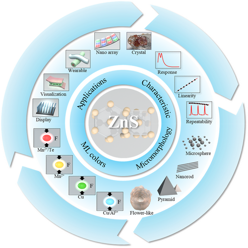
Characteristic, micromorphology, ML colors and application of ZnS particles. Characteristics: photograph of crystal; bimodal ML response44; linearity44; and repeatability.24 Micromorphology: microsphere57; nanorod58; pyramid shape59; and flower-like shape.60 ML colors: ZnS:Cu/Al3+ (blue)61; ZnS:Cu (green)24; ZnS:Mn2+ (orange)23, 52; and ZnS:Mn2+/Te (red).62 Applications: Outdoor display. Reproduced with permission from Ref.63 Copyright 2014, The Royal Society of Chemistry; Pressure visualization. Reproduced with permission from Ref. [25]. Copyright 2015, Wiley-VCH Verlag GmbH & Co. KGaA, Weinheim; Wearable fabric. Reproduced with permission from Ref. [64]. Copyright 2021, The Author(s), under exclusive license to Springer Nature Limited part of Springer Nature; Nano array.65 Reproduced with permission from Ref. [65]. Copyright 2023, Royal Society of Chemistry. ML, mechanoluminescence; ZnS, zinc sulfide.
Since 2015, researchers have focused on optimizing ZnS ML performance for fine applications in different fields. For example, Wang et al. fabricated hand-writable ZnS:Mn2+ films for electronic signatures25; Qian et al. improved the deformability and ML intensity by incorporating SiO2 into ZnS:Mn2+ and ZnS:Cu66; Peng et al. increased the brightness to 2.2 times that of commercial ZnS:Mn2+ by heterogeneous compounding of ZnS:Mn2+ with CaZnOS:Mn2+, and explored the ZnS:Mn2+ bi-phase homojunction structure to enhance its ML capabilities33; Hong et al. prepared nanoscale ZnS:Ag+/Co2+ ML particles for optogenetic therapy, showcasing the diverse applications of ML materials in biomedical fields67; Hou et al. developed bite guards for human–machine interaction based on ZnS particles and introduced artificial neural networks (ANNs) to optimize data quality21; Mukhina et al. clarified the differences in the ML mechanisms of ZnS particles under low and high pressure conditions68; and Zheng et al. investigated the spectral properties of ZnS/CaZnOS:Mn2+ under extreme conditions, suitable for temperature detection under extremely high pressures.34 These studies collectively showcase the multifaceted applications and advances in ML research, ranging from material synthesis to biomedical applications and environmental sensing.
2 CRYSTAL STRUCTURE, DEFORMATION, AND LUMINESCENCE CHARACTERISTICS
The microstructure of crystals and doping ions play a crucial role in determining the luminescence properties of doped ZnS crystals, which, in turn, can further affect their application scenarios. Additionally, their relatively wide bandgap allows for the modulation of luminescence wavelengths and characteristics by doping with various element ions with matching ionic radii.
2.1 Crystal structure
ZnS is not only a typical material for ML applications but also a typical II–VI group semiconductor. Pure ZnS is an n-type semiconductor, although p-type semiconductors can also be obtained by doping ions such as Ag,69 Tm,70 and N.71, 72 At 300 K, the residual electron density in ZnS is approximately 104 cm−3, considerably higher than the expected value produced by thermal ionization in wide-bandgap materials. This suggests that it is a compensating semiconductor characterized by a significantly higher concentration of donor (D) defects compared to acceptor (A) defects.73 In the absence of an external field, the majority of these donors are occupied by electrons and thus remain neutral, while a smaller proportion of ionized donors () offsets the charged acceptors (), thereby ensuring the charge neutrality of the material.68
ZnS exhibits two common allotropes—that is, the hexagonal wurtzite structure (WZ, α phase, non-centrosymmetry) and the cubic zinc blende structure (ZB, β phase, centrosymmetry) (Figure 2). These two structures share a similar single cell. The phase transition temperature from β phase to α phase in undoped bulk ZnS is around 1020°C.74 In the ZB-ZnS structure, tetrahedrally coordinated zinc and sulfur atoms stack in an ABCABC pattern, belonging to the cubic phase and face-centered cubic structure with central symmetry. The lattice parameters are a = b = c = 5.41 Å, Z = 4, and the space group is F-43m, making it an isotropic crystal with a bandgap width of 3.72 eV. In the WZ-ZnS structure, the same elements stack in an ABABAB pattern, belonging to the hexagonal phase and close-packed hexagonal structure. Its lattice parameters are a = b = 3.82 Å, c = 6.26 Å, Z = 2, and the space group is P63mc, making it an anisotropic crystal with a bandgap width of 3.77 eV.75 Additionally, owing to its non-centrosymmetric structure, ZnS exhibits several piezoelectric properties with a piezoelectric constant of 8 pm · V−1.76

Crystal structure of ZnS: (a) zinc blende; (b) wurtzite ZnS; and (c) a single cell. For bond angles, they are 109.5° in both ZB and WZ structures. For bond lengths, in ZB it is L1 = L2 = L3 = L4 = 2.33 Å, and in WZ it is L1 = L2 = L3 = 2.33 Å and L4 = 2.34 Å. WZ, wurtzite structure; ZB, zinc blende structure; ZnS, zinc sulfide.
The size of ZnS particles can affect its bandgap and phase transition temperature. Compared to bulk materials, ZnS nanomaterials have a wider bandgap owing to the quantum size confinement effect of low-dimensional nanostructures.77 Qadri et al. found that reducing the particle size of ZnS crystals to the nanoscale lowers the phase transition temperature.74 In their experiments, the mixture of α and β phases in nano ZnS began to appear at temperatures as low as 350°C, much lower than the typical 1020°C. Additionally, with increasing annealing temperature, the particle size increased considerably, ranging from 2.8 to 243 Å.74
Apart from particle size, the phase transition of ZnS crystals is also related to pressure,78 temperature,79 doping,79 and preparation details.80 For example, Wang et al. proposed that the irreversible phase transition from the WZ phase to the ZB phase occurred at pressures >14 GPa in ZnS:Mn2+/Eu3+.78 Feng et al. mentioned that thorough ball milling of raw materials before sintering could reduce the required temperature for obtaining WZ-structured ZnS.80 Wang et al. explored the influence of the proportion of Mn2+ in the ZnS host on the phase transition.79 They synthesized nanorod-shaped ZnS systems via the hydrothermal method and explored the correlation between the β-phase proportion and the intensity of ML and PL. By adjusting the concentration of Mn2+ doping and the annealing temperature, it was possible to control the ratio of the two phases. Moreover, they indicated that the sample did not exhibit ML properties at calcination temperatures below the required levels.
2.2 Deformation properties related to microstructure
Oshima et al. discovered that ZnS single crystals could exhibit extraordinary plastic deformation effects at room temperature (297 K) in a completely dark environment, achieving a strain of εt = 45%, without undergoing fracture.81 However, when exposed to ordinary light or 365-nm ultraviolet light, the sample quickly fractured after exceeding its plastic deformation point (Figure 3a,b). This phenomenon could be attributed to the fact that the inorganic semiconductors were typically hard and brittle. During deformation, the optical bandgap of the crystal decreased from 3.52 to 2.92 eV (Figure 3c,d), and the crystal changed in color from colorless to gradually becoming orange. This suggested that the optical gap depended on the magnitude of deformation, owing to the introduction of dislocations in the deformed sample. Dislocation core regions in the crystal could have different energy band structures compared to the dislocation-free regions.82
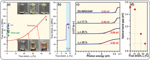
Characterization of plastic deformation. (a) Stress–strain curves of ZnS single crystals under various lighting conditions: UV light (365 nm) (blue line), white light (green line), and complete darkness (red line). (i) An undeformed specimen. (ii, iii) Specimens subjected to deformation under white light and UV light. (iv–vi) Specimens experiencing extensive deformation in complete darkness, reaching (iv) εt = 11%, (v) εt = 25%, and (vi) εt = 35%. (b) Stress-strain curve obtained from deformation at εt = 10% in complete darkness, followed by further deformation under UV light. (c) Absorption characteristics comparison between an unaltered specimen and specimens deformed up to εt = 11%, 25%, and 35% under complete darkness. E, photon energy; α, absorption coefficient. (d) Change in the optical bandgap corresponding to varying deformation strain. Reproduced with permission from Ref. [81]. Copyright 2018, The American Association for the Advancement of Science. ZnS, zinc sulfide.
Further microstructural characterization elucidated the detailed processes involved. Based on the X-ray diffraction (XRD) results, the initially undeformed ZnS crystals exhibited approximately 50% twinning formation (Figure 4a–e).83 As plastic deformation reached around 10% strain, accompanied by changes in the crystal domain volume—that is, the disappearance of twinning—further strain increases in darkness resulted in almost constant crystal domain volume. During the initial stages of plastic deformation, the movement of the crystal domain boundaries and the associated changes in the crystal domain volume were caused by the slip of inter-domain boundary dislocations. During the later stages of plastic deformation, the crystal domain volume remained constant, and an increase in the number of paired partial dislocations was evident as the plastic strain increased (Figure 4f–h). The transition in dislocation behavior could originate from an increase in the crystal domain volume—that is, the disappearance of twinning—leading to the formation of paired partial dislocations.

(a) Schematic representation of the XRD experiments. (b, c) XRD data obtained from an initially pristine, undeformed ZnS crystal. The inset in (c) offers a real-space view of the twin formation. (d, e) The crystal orientations of Domain 1 and Domain 2, corresponding to the green and blue square indices in (b), respectively. (f–h) Bright-field scanning transmission electron microscopy images captured from the 〈111〉 direction for both undeformed and deformed ZnS (εt = 11%, 25%) in darkness, respectively. The schematic representations below indicate dislocations with distinct Burgers vectors, with arrows representing the Burgers vectors of b = 1/6<112>. (i–l) Bright-field TEM images observed from the [110] direction under different conditions: deformation in darkness: εt = 0%, 11%, and 25%; deformation under light: εt = 3%. (m, n) HRTEM images corresponding to (i and k), respectively. (o, p) Diffraction patterns acquired from the zone axis [110] for the undeformed and deformed ZnS (εt = 25%). The green hexagons represent the diffraction pattern of a ZB structure when viewed along [110]. Reproduced with permission from Ref. [83]. Copyright 2023, Acta Materialia Inc. Published by Elsevier Ltd. HRTEM, high-resolution transmission electron microscope; TEM, transmission electron microscopy; XRD, X-ray diffraction; ZB, zinc-blende; ZnS, zinc sulfide.
To validate the changes more directly in the domain volume of Domain 1 and Domain 2 (Figure 4b,c) measured by XRD during plastic deformation, transmission electron microscopy (TEM) observations of both undeformed and deformed specimens were conducted. In darkness, TEM images showed the volumes of either domain (Domain1 or Domain2) tended to increase as the plastic strain increased (Figure 4i–k). Moreover, the high-resolution transmission electron microscopy images and XRD results identified the two-type domains having a twin relationship (Figure 4m,n). Additionally, diffraction patterns were captured from the zone axis [110] for both undeformed and deformed sample (εt = 25%). The diffraction analysis of the undeformed sample revealed twin formations on {111}, while one of the two patterns from the zincblende structure, which had varying crystal orientations, nearly vanished following plastic deformation at εt = 25%. It is evident that the volume ratios of the observed black- and white-contrast areas in the TEM images (Vol.(b)/Vol.(w)) of the undeformed specimen are almost equal to 1, which deviate considerably (reaching approximately 1/6) in the specimen deformed up to εt = 25% (Figure 4o,p). By contrast, under light conditions, Figure 4l shows that a TEM image captured from an area displaying slip lines in the specimen, which was deformed up to εt = 3% under UV light illumination. It is worth mentioning that the Vol.(b)/Vol.(w) differs considerably from the others, approaching roughly 1/4 (Figure 4l).
In conclusion, it is evident that the crystal domain volume changed locally, indicating that local deformation was caused by the motion of boundary dislocations, similar to the initial deformation stages in darkness. The mobility of dislocations interacting with photoexcited charge carriers depends enormously on dislocation characteristics—that is, the atomic species in the dislocation core and the dislocation direction. The dependence of dislocation characteristics on their mobility can lead to non-uniform plastic deformation under light conditions.
When subjected to external forces, the WZ-crystal structure is prone to deformation, leading to the separation of positive and negative polarization charge centers and the generation of a polarization field. This field drives trapped electrons within crystal defects to move to the conduction band, thereby forming electron–hole pairs. The energy released from this process is transferred to the luminescent centers through non-radiative recombination, resulting in luminescence. Although the ZB-crystal structure is a centrosymmetric crystal and typically lacks piezoelectricity—often considered essential for solid materials to exhibit ML—several studies have indicated that piezoelectricity may not be indispensable. For instance, Ma et al. reported that Mn2+-doped ZB crystals also exhibited self-recoverable ML (RML) characteristics. They proposed that this phenomenon was attributed to the transfer of electronic energy to luminescent centers during the process of chemical bond reconstruction, leading to the emission of excited light.84 This topic will be discussed in detail in Chapter 3.
2.3 ML and mechanical quenching (MQ)
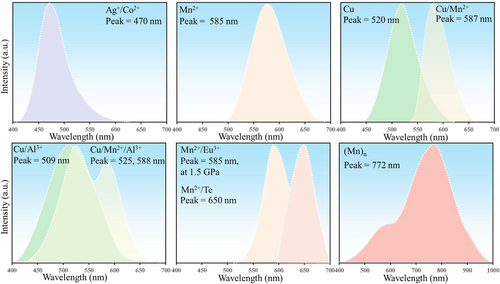
The intense ML in ZnS typically requires doping to occur. Undoped ZnS crystals exhibit weak PL and EL and exhibit little ML owing to the absence of impurity energy levels. Commonly used doping ions that can act as luminescent centers include Mn2+,63, 66, 85-87 Cu+,21 Cu2+,56, 88-90 Cu/Cl,86 Mn2+/Te,62, 91 Mn2+/Li+,92 Mn2+/Cu,56 Ag+/Co2+,93 Cu/Al3+,61, 86 and Cu/Mn2+/Al3+ (Figure 5, Table 1).61 The emissions in the visible light band are bright and clearly visible, especially the blue-light emission (which is unrivaled in brightness compared to other ML materials), thereby enabling the realization of white-light ML emission by combining three colors.63, 100 These advantages have also enabled ZnS to rapidly achieve widespread commercial use in the field of ML.
| Phosphor material | Dopants | λML [nm] | Condition | Refs. |
|---|---|---|---|---|
| α-ZnS/PDMS | Mn2+ | 585 | 1050°C/2 h | [86] |
| α-ZnS/Au/PMN-PT | Mn2+ | 590, 684, 772, 868 | Laser deposition | [95] |
| β-ZnS | Mn2+ | 590 | 900°C/2 h | [84] |
| Bi-phase-ZnS/PDMS | Mn2+ | 590 | 1010°C/2 h | [84] |
| ZnS/PDMS | Cu+ | 475 | Purchase (from LONCO) | [21] |
| α-ZnS (bulk crystals) | Cu/Cl | 517 | Thermal evaporation | [86] |
| α-ZnS/PDMS | Cu | ∼517 | Purchase (GG45, from Osram Sylvania Inc.) | [63, 89] |
| β-ZnS/PDMS | Cu | 520 | Purchase (GGS42, from Osram Sylvania Inc.) | [24] |
| Bi-phase-ZnS/PDMS | Cu | 513 | Purchase (D512c, Shanghai Keyan Optoelectronic Technology Co., Ltd.) | [96] |
| α-ZnS/PVDF | Cu/Mn2+ | 593 | Purchase | [97] |
| β-ZnS/PDMS | Cu/Mn2+ | 587 | Purchase (GGS12, from Osram Sylvania Inc.) | [56] |
| β-ZnS | Cu/Mn2+ | 580 | 1050°C/3 h | [98] |
| α-ZnS/Fe-Co-Ni/PDMS | Cu/Al3+ | 509 | Purchase | [61] |
| α-ZnS/Fe-Co-Ni/PDMS | Cu/Mn2+/Al3+ | 525, 588 | Purchase | [61] |
| α-ZnS | Mn2+/Te | 650 | 1150°C/12 h | [62] |
| β-ZnS (nanoparticles) | Mn2+/Te | 650 | 850°C/10 h | [91] |
| α-ZnS | Mn2+/Li+ | 580 | 1050°C/3 h | [92, 98] |
| α-ZnS | Mn2+/Eu3+ | 585 | 1126.85°C/3 h | [78] |
| α-ZnS (nanoparticles) | Ag+/Co2+ | 470 | 800°C/3 h | [93] |
| ZnS/PDMS:DCJTB | - | 600 | - | [99] |
- Note: The symbol “-” indicates that this case is either not applicable or not mentioned in the article.
- Abbreviations: α-ZnS, the WZ phase; β-ZnS, the ZB phase; DCJTB, 4-(dicyanomethylene)-2-t-butyl-6-(1,1,7,7-tetramethyljulolidyl-9-enyl)-4H-pyran; PMN-PT, Pb(Mg1/3Nb2/3)O3-xPbTiO3; WZ, wurtzite structure; ZB, zinc blende structure.
Metal ions typically replace Zn atoms in the ZnS crystal lattice and serve as luminescent centers, whereas Cl− ions fill defect levels within the ZnS crystal, thereby considerably altering the local piezoelectric constants around luminescent ions and making it easier to produce ML under pressure owing to piezoelectrically-induced detrapping of the charge carriers.86, 101, 102 Currently, the strongest luminescence intensity among ZnS materials is associated with the doping of Mn2+ ions, which has a luminescence peak at 585 nm (attributed to electron transitions from the 4T1-6A1 level of Mn2+).23 Another common dopant element is Cu. Although it has exhibited blue, green, and orange ML emissions, as shown in Hou et al.'s research (ZnS:Cu+@ Al2O3 exhibits an ML peak at 475 nm, ZnS:Cu2+@Al2O3 at 525 nm, and ZnS:Cu2+/Mn2+@Al2O3 at 595 nm),21 its valence state and mechanism remain controversial.63 First, Cu+ and/or Cu2+ could be involved in the ML process.103 Second, the extraction process causing the blue emission remains unclear.24 The PL spectra show that ZnS:Cu has two emission bands (blue and green).104 The green emission originates from the transition from the shallow defect state to the t2 state of Cu.104 The blue emission has been attributed to various factors—such as the association with the e state,105, 106 the transition from the CB edge of ZnS to the acceptor-like t2 state of Cu,104 or native defect states,107 as Peng et al. determined that undoped samples also exhibited blue emission near 450 nm.107 The introduction of Al could also have a more complex effect on the ML of ZnS:Cu. For example, the overall ML color of ZnS:Cu/Al3+ changes from green to blue light under high-frequency forces.108 Additionally, it has been reported that coating the surface of ZnS:Cu with Al2O3 is necessary to exhibit ML properties.109
Beyond doping, ML can also be influenced by the phase of ZnS (Table 1). Generally, the WZ phase (which forms at high temperatures), displays a stronger ML intensity owing to its non-centrosymmetric crystal structure. However, for ZnS, the total energy difference between the WZ and ZB phases is minimal, making it a polymorphic material prone to stacking faults and mixed phase formation (WZ–ZB).110 This propensity can lead to variations in experimental results, as the precise proportion of the phases within samples is often insufficiently analyzed. Consequently, the interaction between the two phases in ML behavior does not merely reflect a straightforward sum of their individual contributions but involves a more intricate coupling mechanism.68, 110-112 This complexity suggests that the interplay between phases in ML requires additional detailed study to fully understand its dynamics and implications.
Here, we list several results of the relationship between the phase and ML from past research, as shown in Table 1. It is evident that ML has been reported in both WZ and ZB phases for ZnS:Mn2+,84, 86 ZnS:Cu,24, 89 ZnS:Cu/Mn2+,56, 98 and ZnS:Mn2+/Te.62, 91 Specifically, doping and particle size are also factors that can influence the existence of ML. For example, bulk crystals of WZ-ZnS:Cu/Cl exhibit plastico-ML (PML) instead of elastico-ML (EML); microcrystals of WZ-ZnS:Cu/Al3+ exhibit considerable EML. Finally, in nanocrystals, WZ-ZnS:Ag+/Co2+ exhibits UV-RML.93
The ML spectra of ZnS can be influenced by the frequency and magnitude of the applied stress. This has been validated by multiple research groups, although the methods they used to vary the stress frequency and magnitude differ. Here, we list some of the conclusions observed. Through the high-pressure testing system (specifically mentioned in Section 5.3), Zheng et al. applied high pressure to ZnS:Mn2+/Eu3+ and found that under an applied stress frequency of 0.5 GPa · s−1, increasing the stress from 2 to 3.6 GPa results in the ML peak shifting from 585 to 615 nm.78 High-frequency mechanical (or electrical) signals typically cause the spectrum to shift toward blue, the extent of this influence differing according to the doping ions. For instance, with a stretching–releasing testing system, jeong et al. found that the ML peak of ZnS:Cu/Mn2+ remains virtually unchanged when the stretching–releasing circle per minute (S–R cpm) increases from 200 to 500 (Figure 6a). Moreover, its EL peaks do not shift when the electrical frequency increases from 80 Hz to 10 kHz (a sinusoidal voltage, 170 V).56 However, under another doping condition, ZnS:Cu, it exhibits a 3-nm blue shift under the same frequency of S–R cpm (Figure 6b),24 and its EL peak changes from 508 to 460 nm as the electrical frequency increases from 50 Hz to 20 kHz at a fixed applied voltage of 100 V.113 Subsequently, Zhou et al. were able to observe spectral changes under high-frequency mechanical signals (in the kHz range) by applying high-frequency electrical voltages to piezoelectric materials, revealing the influence of high-frequency forces on the spectrum.108 For ZnS:Cu/Al3+, with rectangular wave voltage with fixed strength of 165 V, an initial increase in frequency led to enhanced ML in both the blue and green bands, with the blue band showing a more substantial increase, surpassing the green band in intensity at 3.3 kHz, with both bands beginning to quench at 48 kHz (Figure 6c,d). For ZnS:Mn2+, with rectangular wave voltage with fixed strength of 200 V, an increase in frequency initially led to enhanced ML in the orange band, peaking at 4 kHz and almost disappearing at 9 kHz; moreover, as the frequency continued to increase, near infrared (NIR) ML began to dominate, peaking around 30 kHz, and began to quench with further frequency increases (Figure 6e,f).
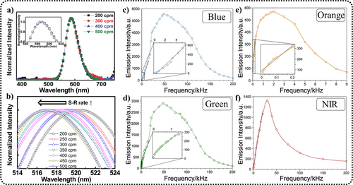
Frequency response of the EML spectral shape and intensity. (a) ZnS:Cu/Mn2+; Reproduced with permission from Ref. [56]. Copyright 2013, WILEY-VCH Verlag GmbH & Co. KGaA, Weinheim. (b) ZnS:Cu; Reproduced with permission from Ref. [24]. Copyright 2013, American Institute of Physics. (c, d) ZnS:Cu/Al3+ (blue and green light); (e, f) ZnS:Mn2+ (orange and NIR light). For samples (c–f), the voltage waveform applied to the piezoelectric materials is a rectangular wave with an amplitude of 200 V. Reproduced with permission from Ref. [108]. Copyright 2022, Wiley-VCH GmbH. EML, elastico-ML; NIR, near infrared.
Upon analysis, it was concluded that the blue shift in the ZnS:Cu/Al3+ spectrum was due to increased electron–hole recombination rates for both Vs (S vacancies)-CuZn (Cu replacing Zn) (blue light) and AlZn (Al replacing Zn)-CuZn (green light) pairs; whereas for ZnS:Mn2+, the blue shift was caused by high-frequency signals promoting the formation of (Mn)n clusters (n = 2–6) and the energy transfer from excited Mn2+ ions to (Mn)n clusters.95, 108 Finally, the saturation and subsequent quenching of ML in both cases could be attributed to the carrier recombination rate failing to match the excitation frequency.
The ML of ZnS possesses an exceptionally low threshold. However, this threshold can be influenced by several factors, including the doping ions,86 particle size,86 surface morphology,114 crystal structure,68, 110 testing conditions (whether compounded with a matrix, the rate of load application), and the structure of the fabricated devices.115, 116 Consequently, variations in threshold values are evident across different studies. Here, data observed in several seminal studies are summarized. In the research conducted by Chandra et al.,86 it was mentioned that for ZnS powder, smaller particles led to a lower threshold. For example, ZnS:Mn2+ bulk crystals (diameter: 1.2 mm, length: 3 mm) exhibited an EML threshold of 20 MPa, whereas its microcrystals had an EML threshold of 1 MPa. In the case of ZnS:Cu/Cl, the bulk crystals (2 × 2 × 4 mm3) only exhibited PML with a threshold of 30 MPa, whereas microcrystals exhibited EML with a threshold of 1.5 MPa. On the one hand, bulk crystals are less prone to deformation and have fewer internal defects near impurity centers, which can lead to a higher ML threshold and a lack of EML in ZnS:Cu/Cl. On the other hand, the introduction of Cl ions into ZnS:Cu results in the filling of negative ion vacancies by the Cl− ions.117 Consequently, the number of local dipoles is reduced, leading to the disappearance of EML.117 Wei et al. fabricated thin-film structures of ZnS:Cu using polymethyl methacrylate (PMMA) and fluorinated ethylene propylene (FEP), measured the ML through friction and discovered that the ML threshold could be even lower than 10 kPa. They attributed this extremely sensitive ML to triboelectroluminescence (TIEL).115 In the study by Mukhina et al.,68 it was found that some ZnS:Mn2+ microcrystals had a threshold below 1 MPa, with a few microcrystals exhibiting a threshold of just 233 ± 60 kPa. It is noteworthy that in their experiment, 44 samples of ZnS:Mn2+/PDMS were tested, with the ZnS:Mn2+ having a diameter of 4.6 μm, various surface structures, and a load application rate of 0.125 μm · ms−1. They attributed the exceptionally low thresholds observed in certain particles to the enhancement of the local piezoelectric field resulting from the WZ–ZB phases. Subsequent research by Wang et al. proposed a similar viewpoint, suggesting that ZB-ZnS stacking faults in WZ-ZnS crystals caused band bending, which reduced the gap between shallow donors and the conduction band, thereby enabling the material to generate ML under minimal stress excitation.110 In this model, the variability in threshold values among different ZnS particles could be explained by the differing relative proportions of the WZ and ZB phases, leading to varying degrees of conduction band bending and, consequently, different ML thresholds.
ZnS ML also exhibits linear and quadratic characteristics. Linearity refers to the fact that the emitted ML intensity is proportional to the magnitude of (P-Pth)2.118 Overall responses can be fitted with linear functions, with the slope and intercept of this function varying depending on factors such as the doping and testing conditions (Figure 7a).86 Considering that ML responds to the strain rate—that is, dynamic forces are needed to trigger ML—the response curve can also be influenced by the strain rate (the amount of deformation per unit time). For instance, Jeong et al. observed considerable differences in ML intensity when applying stress at strain rates ranging from 200 to 500 cpm (Figure 7b).24 However, controlling the strain rates, especially under rapid force impact, can be challenging. Hence, current research commonly employs the stress magnitude as the independent variable for the response function. Additionally, the quadratic characteristic imply that during the EML process, a second ML peak emerges after releasing the applied pressure (Figure 7c),44 which is more intense than the light emitted during pressure application.23 This could be due to higher strain rates upon the release of pressure.86 However, the generation and appearance of this secondary ML peak are notably quicker, posing a challenge for its precise capture and characterization.
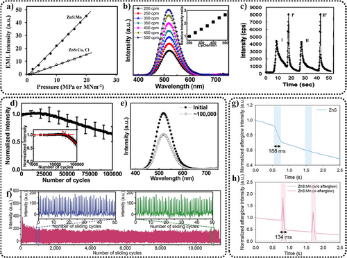
(a) Relationship between EML intensity and pressure of ZnS:Mn and ZnS:Cu/Cl (pressing rate = 10 MPa · ms−1). Reproduced with permission from Ref. [86]. Copyright 2016, Elsevier B.V. (b) Relationship between ML intensity and strain rate (S–R cpm) of ZnS:Cu/PDMS. Reproduced with permission from Ref. [24]. Copyright 2013, American Institute of Physics. (c) ML response of ZnS:Mn nanoparticles (coated on quartz plate, compression stress = 500 N, compression stress rate = 0.10 mm · min−1). Reproduced with permission from Ref. [23]. Copyright 1999, American Institute of Physics. (d) The ML intensity variation of ZnS:Cu film during 100,000 stretching–releasing cycles, (e) Comparison of the ML intensity of ZnS:Cu film in the initial state and after 100,000 stretching–releasing cycles. Reproduced with permission from Ref. [24]. Copyright 2013, American Institute of Physics. (f) The ML intensity variation of ZnS:Mn2+ films during 10,000 bending cycles. Reproduced with permission from Ref. [25]. Copyright 2015, WILEY-VCH Verlag GmbH & Co. KGaA, Weinheim. (g, h) The MQ phenomenon in PVDF-HFP/ZnS and PVDF-HFP/ZnS:Mn2+ patches under mechanical force. Prior to the experiment, both samples were exposed to UV light for 5 s, with blue and red regions indicating the repeated application of the same pressure (10 MPa). The gray line in (h) represents the ML of PVDF-HFP/ZnS:Mn2+ patches without afterglow (under the same mechanical force condition but being left for 30 min after UV pre-radiation) The ML intensity observed was comparatively lower than that seen with afterglow. Reproduced with permission from Ref. [119]. Copyright 2024, Wiley-VCH GmbH. EML, elastico-ML; ML, mechanoluminescence; MQ, mechanical quenching; PDMS, polydimethylsiloxane; PVDF-HFP, polyvinylidene fluoride-hexafluoropropylene; ZnS, zinc sulfide.
The rise and fall times of ZnS ML are typically in the microsecond range, but results can vary owing to different testing methods. In Chen et al.'s research, the material was mixed with epoxy resin, and a force signal was applied using the drop-ball method. They measured the ML lifetime of ZnS:Mn2+ to be approximately 0.97 ms, with the ML intensity curve undergoing a rapid increase to a peak at approximately 35 μs, followed by a slow decay over several milliseconds.120 In Zhou et al.'s study, the material was compounded using a UV-curable adhesive matrix, and a high-frequency force signal was applied using a piezoelectric material.108 They found that the rise and fall times were both related to the frequency of the applied force. When the excitation frequency was below 12 kHz, the rise and fall times were 9.7 and 35.1 μs, respectively. As the excitation frequency increased, the decay process was interrupted by the strain release, and the fall time was no longer calculated. The rise time began to gradually decrease only when the excitation frequency exceeded 30 kHz, reaching 7.2 and 5.8 μs at 40 and 50 kHz, respectively.108
The repeatability of ML is also crucial for its application. Initially, Xu et al. conducted sliding-stress tests on crystal thin films of ZnS.23 Later, Jeong,24 Wang,25 Wei,115 Peng,33, 35, 84, 121 and others performed repeatability tests under sliding/stretching/bending conditions on films compounded with ZnS powder (Figure 7d–f), confirming its excellent repeatability.24
It is worth mentioning that ZnS exhibits an effect opposite to ML—known as MQ119—which refers to the phenomenon where the afterglow (AL) of the material diminishes after being subjected to stress (Figure 7g,h). The principle behind this phenomenon shares certain similarities with ML, the main difference lying in the stress-induced piezoelectric field driving electrons to recombine with holes at non-radiative centers. Observing MQ requires pre-charging the material with UV light to generate AL. Upon applying stress, a momentary ML occurs, followed by a weaker AL at the stressed sites compared to unstressed ones, indicative of MQ. Pre-charging also leads to stronger ML compared to when not pre-charged, although the enhancement diminishes with the continued application of stress. This characteristic is very similar to the ML of SrAl2O4:Eu2+,5 suggesting that ZnS's MQ can be seen as having dual modes of generation—that is, mechanical energy converted to light energy and mechanical energy inducing the release of stored energy in the form of light, with the latter being less pronounced.
It is important to note that MQ is more easily observed in undoped ZnS,119 but the introduction of Mn doping induces ML in the material, reducing the AL, which in turn makes the MQ effect more likely to be overlooked.
2.4 Multi-stimuli responsive luminescence
ZnS exhibits multimode luminescent characteristics beyond ML, including PL, EL, thermoluminescence (TL), X-ray-induced luminescence (XIL), and cathodoluminescence (CL) (Figure 8). These luminescence modes share close ties with ML, their spectra being consistent with that of ML, so playing an important role in understanding the underlying mechanism within ML.
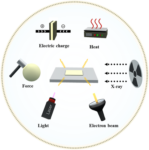
Multimodal luminescence of zinc sulfide.
PL refers to the phenomenon in which luminescent materials emit light after absorbing photons (electromagnetic radiation). If the emitted light has a shorter wavelength than the excitation light, it is called down-conversion or down-shifting luminescence; conversely, if the emitted light has a longer wavelength, it is known as up-conversion luminescence or anti-Stokes photoluminescence, which requires the simultaneous absorption of two or more photons. Down-shifting luminescence is more common in ZnS-based fluorescent materials and can be observed in various main group, transition metal, and lanthanide ion-doped ZnS materials, such as Mn2+,23 Co2+,122, 123 Cu+/2+,21, 24 Sb3+,124-126 Pb2+,127-130 Al3+,126, 131-133 Sn2+,126, 134, 135 Bi3+,136 Ag2+,100 Au+,137-139 and Ln2+/3+ = Eu2+/3+, Sm3+, Tb3+, Er3+,140, 141 among others. Their spectra essentially cover the visible light range. Additionally, up-conversion luminescence can be observed in ZnS nanocrystals doped with various lanthanide ions, such as Er3+,142 Yb3+,143 and Ho3+,144 among others. The Zn2+ and S2− ions in ZnS are also prone to defects during the synthesis process, introducing intrinsic defects and trap levels for capturing electrons and holes, characteristics that contribute to the versatile luminescent properties of ZnS materials.
Similar to PL, when a material emits light owing to X-ray radiation, it is referred to as XIL. X-rays can induce phenomena such as the photoelectric effect and Compton scattering, and pair production of electron–hole pairs within the atomic lattice of the luminescent material, generating a large number of hot electrons and deep holes. These low-energy charge carriers gradually migrate to luminescent centers, leading to luminescence emission. Materials exhibiting XIL properties are also called scintillators. As the excitation mechanisms for XIL and PL are similar, their spectra are also similar, such as the XIL spectrum of ZnS:Cu/Co nanoparticles,145 which falls in the range of 400–650 nm with a peak at 510 nm, closely matching the PL spectrum.
Moreover, ZnS exhibits excellent EL properties, with ZnS:Cu demonstrating superior performance when subjected to an external alternating current (AC) electric field. This phenomenon was first discovered in 1936 when Destriau dispersed the ZnS:Cu phosphor in castor oil.146, 147 Usually, it is necessary to formulate a multi-layer structure to achieve ZnS alternating current electroluminescent (ACEL). The core phosphor layer is either the ZnS powder itself (using the deposition method) or a composite of ZnS, dielectric particles (e.g., BaTiO3 148), and matrix (e.g., resin,148 polyvinylidene fluoride [PVDF],149 or PDMS150). Structurally, ACEL devices can be classified according to their dielectric layers into two types—that is, symmetric and asymmetric structures (Figure 9).
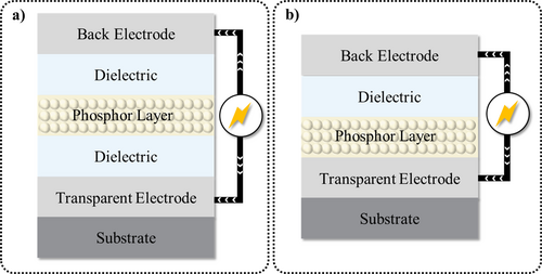
Schematic illustrations of symmetric (a) and asymmetric (b) structures.
In symmetric structures, the electron and hole generation layers can be inserted between the phosphor layer and dielectric to facilitate carrier generation. In simpler asymmetric structures, holes and electrons can be injected alternately from the same electrode in different electric field directions.151
The dielectric layer and CuxS needles play important roles in the process of ZnS ACEL. Under the influence of an AC electric field, defects at the interface or within the phosphor layer are activated as charge carriers and subsequently injected into the phosphor layer. As shown in Figure 10a, the dielectric directly contacts ZnS, creating substantial interfacial states with energy levels distributed within the forbidden band gap of the semiconductor. These activated hot electrons are injected into the conduction band through tunneling and/or field-enhanced thermal excitation of trapped electrons (Figure 10a). Conversely, the CuxS needles not only facilitate the formation of Schottky barriers between CuxS and the ZnS semiconductor but also intensify the local electric field by one to two orders of magnitude. This intense local electric field causes electrons and holes to be injected from both ends of the CuxS needles through tunneling (Figure 10b).
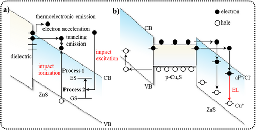
(a) Energy band diagram when a dielectric material and a semiconductor are in contact. (b) Energy band diagram of the simultaneous injection of electrons and holes from the opposite ends of a CuxS needle into the surrounding ZnS:Cu/Cl lattice. CB, conduction band; ES, excited state; GS, ground state; VB, valence band. Reproduced with permission from Ref. [147]. Copyright 2021, Author(s).
After carrier injection, theories that explain the subsequent light emission include the impact ionization and impact excitation theories. In the impact ionization theory, high electric fields accelerate thermal electrons to collide with the phosphor lattice, generating electron–hole pairs (Process 1, Figure 10a). These pairs are subsequently captured by donors and acceptors. The recombination of these electrons and holes then produces light emission, or electron–hole pairs transfer their energy to doping ions (such as Mn2+), causing electron transitions to excited states and subsequent light emission upon returning to the ground state. In the impact excitation theory, thermal electrons directly collide with local luminescent centers, exciting ground state electrons to higher energy levels (Process 2, Figure 10a), producing light emission upon their return to the ground state.
TL is a phenomenon where a material emits electromagnetic or ionizing radiation (previously absorbed and stored as photon energy within the lattice defects) when heated. This process is also known as thermally stimulated luminescence. The sources of radiation energy that can be absorbed include visible light, X-rays, β-particles, or α-particle radiation, among others. The TL intensity of ZnS material increases as the crystal size decreases because smaller particle sizes result in increased surface states or defect sites that can trap carriers.152 When heated, more charge carriers are released, combining with holes, and the energy is transferred to the luminescent centers, resulting in enhanced light emission. Additionally, reducing the particle size can increase the overlap between electron and hole wave functions, potentially accelerating the rate of charge carrier recombination, and further enhancing luminescence.152 It is worth noting that the ZnS TL peak does not vary substantially with decreasing particle size, which could be because the trap depth of surface states is insensitive to particle size.153
CL is the phenomenon where luminescent materials emit light when excited by a high-energy electron beam, thus offering higher spatial resolution (up to several nanometers) and applicability to wide-bandgap semiconductors compared to other luminescent methods. CL imaging is a powerful tool for visualizing the spatial distribution of excitons, defects, and other phenomena within a material, thereby facilitating detailed analyses of the crystal lattice and band structure. For the same material, different morphologies, doping ions, and temperature variations can result in different CL spectra.154 Generally, ZB-ZnS exhibits strong and stable 337-nm ultraviolet emission in CL spectra at room temperature.59 Liu et al. studied the morphology, doping, and temperature dependence of one-dimensional ZnS nanostructures in CL.58 Chen et al. successfully synthesized pyramid-structured ZB-ZnS using thermal evaporation, and its CL spectra exhibited strong and stable 337-nm ultraviolet emission, indicating high crystallinity.59 This emission could be attributed to band emission from the ZB structure. Moreover, compared to other structures—such as nanobelts, nanowires, and nanorods—pyramid-structured ZB-ZnS exhibited a lower turn-on field, higher field-enhancement factor, and high stability with low fluctuation of field-emission current, suggesting its potential suitability for optoelectronic applications.59
3 ML CLASSIFICATION AND MECHANISM
Based on the force application method during the ML process, the ML mechanism can be broadly categorized into deformation ML (DML) and tribo-ML (TML). For DML, depending on the extent of deformation caused by the applied force, it can be further divided into three luminescence mechanisms—that is, EML (elastic deformation), PML (plastic deformation), and fracto-ML (FML, fracture of the crystal lattice). For TML, it encompasses various luminescence mechanisms induced by triboelectrification and electroluminescence between solid ML particles and other materials. These mechanisms include electrically induced ML, chemically induced ML, and thermally induced ML.24
Figure 11 shows the classification and relationships of these ML mechanisms.155 EML and TML materials are considered to be the most promising ML materials for practical applications owing to their self-recoverable luminescence properties. For example, ZnS:Mn2+ exhibits only a slight decrease in luminescence intensity after 100,000 repeated stretches.24 Conversely, other materials may exhibit RML but require recharging with additional energy (such as UV light), termed UV-RML. A prime example is SrAl2O4:Eu2+/Dy3+, where ML entails the emission of photons in response to disturbances from external fields such as electric or force fields. The intrinsic mechanism involves the easy release of electrons in a metastable state under external stimuli.5
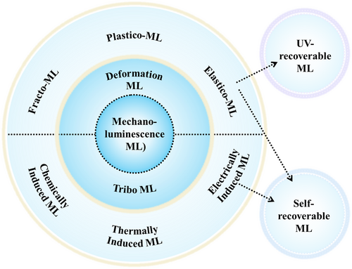
Classification of ML mechanisms. Reproduced with permission from Ref. [155]. Copyright 2021, Elsevier Ltd. ML, mechanoluminescence.
In some research reports, TML is used interchangeably with ML. This is because TML used to be referred to as ML in earlier research.156 To avoid confusion, this paper uses ML to refer broadly to all luminescent phenomena induced by mechanical force, while TML is used to specifically indicate ML induced by friction. Moreover, it is necessary to clarify the specific differences between DML and TML: DML is solely induced by the deformation of the ML material and is independent of the material's properties causing the deformation. Consequently, DML is a physical process, such as luminescence from the fracture of sugar cubes. TML, on the contrary, is related to the interface properties of different materials when they come into contact with deformation, leading to effects like charge generation, heat generation, or chemical reactions.24
Although the classification of ML into two main categories and six subcategories is widely accepted,157 it remains challenging to confirm the specific types of ML involved in the actual processes of all materials and further divide them into their different mechanistic categories. This complexity can also lead to a variety of mechanisms to account for the ML in ZnS. The classical model remains the piezoelectric model, with many new models being improvements based on it. Additional models have proposed various mechanisms, some of which offered explanations for the generation of the piezoelectric field. If the field was generated through dislocations, then it was a dislocation model; if explained through WZ–ZB-phase heterostructures to account for high piezoelectric fields under small pressures, it led to spatial models; if generated through triboelectricity, then it resulted in a triboelectric model. That said, the covalent bond breaking model is somewhat unique. Owing to the non-centrosymmetric structure which lacks piezoelectric effects, this model involves the breaking and reformation of Zn-S covalent bonds and a series of subsequent processes to explain the ML of β-ZnS.
However, no single model can uniformly explain the ML of ZnS in all scenarios (including doping, and grain size, etc.). First, the material can be doped with a rich variety of ions, each potentially having a different pathway and method of internal electron generation and transfer under force. Second, it can be challenging to synthesize purely WZ- or ZB-phase ZnS; the two phases tend to coexist to varying degrees in samples used for testing. The extent of this coexistence and its impact on the mechanistic process require further exploration, with most current models only explaining the ML process of a single phase and lacking in-depth investigation into the impact of bi-phase ZnS. Moreover, tests are often performed on ZnS and organic compounds (for example, ZnS/PDMS). Under the same type of mechanical stimulation (stretching, compression, and friction, etc.), multiple subsequent processes (such as heat generation, deformation, and electric field formation), can occur within the material. Finally, with existing techniques, it can be difficult to directly detect the specific behavior within a material; instead, inferences are made through the material's intrinsic properties, delayed lifetime images, and PL spectra. Consequently, further analysis of mechanisms still requires the development and refinement of experimental facilities and protocols.
3.1 Piezoelectric effect model
The piezoelectric effect model is the most common model used to explain ZnS ML in different doping situations, such as Mn2+,117 (Mn)n,108 Cu,117 Cu/Mn2+,77 Mn2+/Te,91 and UV-RML in ZnS:Ag+/Co2+.93 This model suggests that ML in ZnS is intimately linked to the excitation–deexcitation process of the built-in electric field and luminescent centers during deformation, which is also supported by the consistency observed in the PL, EL, and ML spectra. Regarding the transfer of mechanical energy from ZnS crystals to luminescent centers during the EML process, Chandra et al. noted that when the crystal underwent elastic deformation, the piezoelectric constant near the impurity center increased considerably compared to other positions in the crystal.102 Consequently, with the non-centrosymmetric structure of ZnS, a strong piezoelectric field is generated in the crystal's vicinity, leading to a reduction in trap depth within the crystal. This reduction allows trapped electrons to escape the confines of the traps and move into the conduction band. Some of these escaped electrons recombine with holes, releasing energy that can be transferred to the luminescent center, which then emits energy in the form of light waves. Moreover, the self-recovery characteristic of EML can be achieved through the recapture of carriers drifting in the presence of the piezoelectric field.117 Chandra coined this ML excitation model the “piezoelectrically-induced trap-depth reduction model,” which was also suitable for ML of ZnS crystals of different sizes (bulk crystals, microcrystals, and nanocrystals).94, 158, 159 However, ML is only applicable when the force varies with time rather than being static.102, 160
This model is typically used to explain the orange ML emission of ZnS:Mn2+.94 Although there are partial distinctions in other situations, the main triggering factor is usually the piezoelectric field induced by pressure. For ZnS:(Mn)n, the NIR ML is due to the energy transfer from excited Mn2+ ions to (Mn)n clusters under high-frequency mechanical excitation.108 For ZnS:Cu, the luminescent center is Cu rather than Mn2+.117 For ZnS:Cu/Mn2+, Cu and Mn2+ together act as luminescence centers.77 For ZnS:Mn2+/Te, the EML process involves energy transfer from Mn2+ to Te, where the transition of Te from 3T1 to 1A1 emits red light.161 For ZnS:Ag+/Co2+, UV light excites electrons, which are captured by Co2+ and remain in a metastable state. Pressure-induced piezoelectric fields release electrons from Co2+, transferring energy to Ag+, causing a transition that emits photons with a wavelength of 470 nm.93 Based on the principles of light-emitting diodes, heterojunction structures can considerably enhance the EML intensity of crystals.
Peng et al. combined p-type CaZnOS and n-type ZnS to create a p-CaZnOS/n-ZnS:Mn2+ piezoelectrically-induced luminescent heterojunction crystal. When an external force is applied, the built-in piezoelectric field causes a band offset between the ZnS/CaZnOS heterojunction, increasing the efficiency of electrons escaping from traps into the conduction band and forming electron–hole pairs (Figure 12a,b).
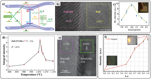
(a) Band bending between heterojunction regions caused by the built-in piezoelectric field. (b) High-resolution TEM image of a heterojunction in a ZnS/CaZnOS particle and a bi-phase junction cut from the edge of a ZnS particle (1020°C, 2 h). (c) Integrated intensity over the 500–750 nm range from ZnS/CaZnOS heterostructures under mechanical excitation at 35 N as a function of ZnS to CaZnOS molar ratios. Inset: Photograph of the sample with the optimal composition under mechanical excitation using a finger. Reproduced with permission from Ref. [33]. Copyright 2020, WILEY-VCH Verlag GmbH & Co. KGaA, Weinheim. (d) The ML integrated intensity of ZnS:2% Mn2+ at different temperatures. The sample is in a pure ZB phase at 900°C, and a bi-phase at 1010°C. The sample with the strongest ML is sintered at 1010°C for 2 h, during which ZnS is in a bi-phase state. (e) A bi-phase junction cut from the edge of a ZnS particle (1020°C, 2 h). Reproduced with permission from Ref. [111]. Copyright 2022, Tsinghua University Press. (f) Integrated intensity over the 500–750 nm range from (3ZnS/2CaZnOS)1-xSrZnOSx:2% Mn2+ heterostructures under mechanical excitation at 30 N as a function of the 3ZnS/2CaZnOS ratio. Insets: ML photographs of the strongest and weakest luminescence. Reproduced with permission from Ref. [162]. Copyright 2023, The Author(s). Published by Elsevier Ltd. ML, mechanoluminescence; TEM, transmission electron microscopy; ZB, zinc blende structure; ZnS, zinc sulfide.
This enhances carrier mobility, thereby substantially increasing the EML intensity. Consequently, the ZnS/CaZnOS heterojunction structure exhibits highly reproducible EML, with an intensity 2.2 times higher than that of commercial ZnS:Mn2+ and 3.5 times higher than that of the classical quaternary EML material CaZnOS:Mn2+. It can emit visible light under a 1 N fingertip force excitation (Figure 12c). Additionally, full-spectrum tunable luminescence has been achieved covering the visible and NIR spectrum by incorporating Mn and lanthanide ions Ln3+ (such as Ce, Pr, Nd, Sm, Eu, Gd, Tb, Dy, Ho, Er, Tm, and Yb) into the structure. Based on the heterojunction principle, bi-phase homojunction ZnS:Mn2+ crystals (WZ and ZB phases) have also been synthesized, which exhibited EML intensities 3–6 times higher than pure WZ-phase ZnS:Mn2+(Figure 12d,e). Furthermore, they reported ML enhancement in SrZnOS using the ZnS/CaZnOS heterojunction, resulting in an EML intensity approximately 60 times higher than SrZnOS:Mn2+ (Figure 12f). Additionally, the ZnO/ZnF2 heterojunction they constructed also considerably enhanced the EML intensity of ZnO:Mn2+.33, 37, 162
3.2 Models related to dislocation motion
Covalent bond breakage-reformation model
The covalent bond breakage-reformation model can be used to explain the ML in β-ZnS:Mn2+. The majority of centrosymmetric crystal structures do not exhibit ML characteristics, because crystals with a center of symmetry undergo uniform deformation when subjected to stress, and the center of positive and negative charge mass remains overlapping, resulting in no polarization and, therefore, no piezoelectric effect. Whereas some centrosymmetric crystals may occasionally display ML, their ML is either caused by the piezoelectric phase of defects or is unrelated to piezoelectric effects, such as luminescence caused by the charge impact on gas molecules within the crystal and defect motion.163
Ma et al. proposed this improved plastic DML model to explain the self-RML in β-ZnS:Mn2+.84 When an external force is applied, defects within the crystal move, causing partial covalent bonds between Zn and S to break. This results in the redistribution of s and p electrons, leading to a considerable number of Zn2+ ions acquiring extra electrons. These extra electrons can be considered to be intermediate states for rebuilding covalent bonds, with an abundance of Zn dangling bonds in the Zn 4s orbital (CB) with extra electrons and extra holes in the S 3p orbital (VB). These conditions are sufficient to excite ML.
They also employed a carrier capture model to explain how carrier energy is transferred to Mn2+. To be specific, Mn2+ is involved in the recombination of electron–hole pairs. When an electron–hole pair migrates near Mn2+, Mn2+ sequentially captures the holes from the valence band and the electrons from the conduction band. This completes the energy transfer from the exciton (electron–hole pair) to Mn2+, resulting in Mn2+ being in an excited state. This process differs from the common pathway where Mn2+ directly transitions from the ground state to the excited state. In this model, there is a brief process of Mn3+ generation, similar to Mn2+ acting as a recombination center for electron–hole pairs.164 Thus, it exhibits high luminescence efficiency. After the ML process is completed, the broken covalent bonds are reformed, allowing ZnS to exhibit good ML repeatability. This explains why the samples with the highest PL and ML do not necessarily have the same Mn2+ doping concentrations (Figure 13).
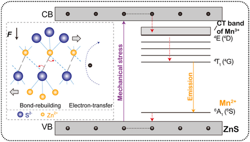
Schematic diagrams of self-recoverable mechanoluminescence mechanisms in β-ZnS:Mn2+. Reproduced with permission from Ref. [84]. Copyright 2020, Elsevier B.V.
The mechanism can be explained through the emission and excitation spectra of β-ZnS and β-ZnS: Mn2+ (Figure 14a). In further experiments, they observed that the β-ZnS sample exhibited a broad UV excitation band at 470 nm, composed of excitonic transitions (ZnS:VB→CB) (I) and a defect-related excitation band centered at 340 nm (II). When monitoring the emission at 590 nm, corresponding to Mn2+, the excitation band of β-ZnS:Mn2+ included excitonic transitions (I), charge transfer transitions (Mn2+ 3d→CB), and a series of d-d transitions centered at 355 nm (II) (Mn2+:6A1(6S)→4E (4D), 4T2 (4D), (4A1,4E) (4G), 4T2 (4G), or 4T1 (4G)) (III).165
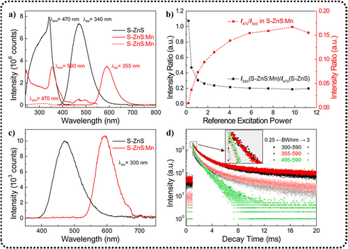
(a) Excitation and emission spectra of S-ZnS and S-ZnS:Mn2+, where S-ZnS is equal to β-ZnS. (b) The relationships between the peak intensity ratios and excitation power. The red dotted line is I470/I590 in S-ZnS:Mn2+. The black dotted line is I590, S-ZnS: Mn/I470, S-ZnS. (c) PL comparison of S-ZnS and S-ZnS:Mn2+ under low excitation power. (d) The luminescence decay curves of 590-nm emission in S-ZnS:Mn2+ under different excitation (300, 355, and 495 nm) with a bandwidth of 0.25 or 3 nm. Inset is the magnification of the selected initial decay. Reproduced with permission from Ref. [84]. Copyright 2020, Elsevier B.V. PL, photoluminescent; ZnS, zinc sulfide.
Two notable facts about β-ZnS:Mn2+ are the disappearing blue emission band under 355-nm excitation and the absence of the defect-related excitation band when monitoring at 470 nm. These observations suggest the presence of an efficient energy transfer process from the defect centers to Mn2+. Considering that ML may not be as efficient as PL in mechanical-to-optical energy conversion, under the condition of a fixed excitation wavelength at 300 nm, by further reducing the excitation power, the intensity ratio of blue to yellow emission (I470/I590) decreases (Figure 14b). At low excitation intensity (approximately 2% of the initial excitation), the blue emission band eventually disappears, resulting in the PL spectrum being similar to the ML spectrum (Figure 14c). Although the blue band caused by defects in β-ZnS and the yellow band caused by Mn2+ in β-ZnS:Mn2+ can be separately excited by 300-nm ultraviolet light, at relatively low excitation power, the efficiency of ultraviolet-to-yellow energy conversion is substantially improved. Consequently, they suggest that the RML process in β-ZnS:Mn2+ is similar to the inter-band excitation PL process involving Mn2+ under weak excitation, rather than being primarily influenced by any point defects.
To describe the luminescence mechanism, they further studied the luminescence decay behavior in β-ZnS:Mn. By adjusting the bandwidth to change the laser intensity (0.25 and 3 nm), they compared the luminescence decay curves (Figure 14d). Ignoring the later slow decay, after magnifying the initial decay curves (see inset in Figure 14d), they found that under weak excitation of band I or band II, the decay curves completely overlapped. The longer decay lifetimes compared to band III can be attributed to additional trapping and detrapping processes between the defect levels and the CB. Under strong excitation of band I or band II, accelerated decay of the 590-nm emission was evident owing to increased non-radiative electron–hole recombination. In conclusion, the above spectral results validated the rationality of their proposed ML model.
ML spatial models
To fill the research gaps, Mukhina et al. revealed the existence of three different ML mechanisms in single ZnS particles under low stress (<8.1 MPa).68 They referred to these mechanisms as the ML induced by stacking faults exciton fields (Pz mechanism), ML induced by fully or quasi-reversible fault bending (μD mechanism), and ML induced by irreversible fault slip at higher pressures (D mechanism) (Figure 15). When the stress was below 8.1 MPa, ML generation was dominated by the Pz mechanism, and the μD mechanism also came into play. By contrast, at pressures above 8.1 MPa, charged fault motion became the primary source of excitation. This model could explain the EML in ZnS:Mn2+ at extremely low pressures (≈233 kPa). The mechanism relies on the local enhancement of the piezoelectric field produced by the stacking faults' interfaces of WZ and ZB phases along the c-axis direction of the ZnS crystal, where some interfaces lack electrons, enhancing the local piezoelectric field generated when an external stress is applied.68
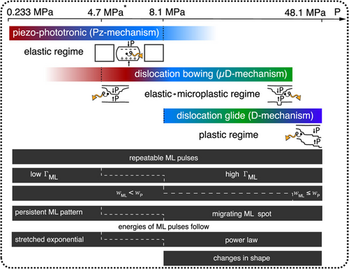
ML mechanisms at different pressure ranges with corresponding properties. ΓML, wML, and wP denote the ML emission rate, width of the ML pulse, and width of the pressure pulse, respectively. *Provisional limit of the microplastic regime defined by the lowest pressure at which the μD-component is observed in experiments. Reproduced with permission from Ref. [68]. Copyright 2021, American Chemical Society. ML, mechanoluminescence.
Assuming that the EML of ZnS requires a sufficiently large electric field for excitation, in cases where the electric field intensity from the piezoelectric effect is insufficient, alternative sources of enhanced electric fields need to be identified. Previously, it was believed that the EML of ZnS originated solely from the piezoelectric effect of the pure WZ phase.68 However, Mukhina et al. observed the phenomena of WZ–ZB phase alternation in ZnS and proposed that such microstructural heterogeneity could generate a sufficiently strong intrinsic electric field. This, when stressed, could induce intense EML. In the faulted structure depicted in Figure 16, ZB is inserted into the WZ, forming a WZ–ZB–WZ structure.
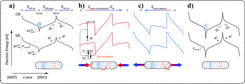
ML mechanisms for a structural unit WZ/ZB/WZ, under different conditions: (a) without external stress, (b) compressed, (c) dilated, and (d) after multiple emission cycles. Red pluses and blue minuses denote polarization charges induced by electric fields and localized states. Blue and empty red circles illustrate free electrons and holes, respectively. Gray dotted lines in panels (b–d) depict band structures prior to pressure application. Reproduced with permission from Ref. [68]. Copyright 2021, American Chemical Society. ML, mechanoluminescence; WZ, wurtzite structure; ZB, zinc blende structure.
In Figure 16a, owing to the absence of inversion symmetry along the c-axis, an electric field (EWZsp) is generated within the WZ phase. Owing to the reverse piezoelectric effect, the insertion of the ZB phase produces an electric field (EZBpiezo) in the opposite direction. Consequently, an intrinsic sawtooth potential (Ψsaw) is generated, causing free carriers (electrons) to drift toward the positive pole, leaving behind vacant D+ and A0 energy levels to compensate for the intrinsic field. The most likely candidates for the A0 center are the shallow hole states in S vacancies, which are involved in defect-related ZnS luminescence at room temperature.
During compression (Figure 16b), a unipolar piezoelectric field pervades the entire particle. It aligns with the intrinsic field direction in the ZB phase and opposes the intrinsic field direction in the WZ phase. Consequently, the overall internal fields rearrange, resulting in a change in Ψbi. The most important alteration occurs at the WZ/ZB interface owing to intrinsic compensation, leading to electron depletion. Here, the potential profile (Ψpiezo) induced by the piezoelectric effect cannot be screened by free electrons, and the bands of the WZ and ZB phases could contain relative potential jumps reminiscent of a piezoelectric p–n junction.173, 174 Hence, the increase in the local barrier owing to this phenomenon could exceed what is predicted by the intrinsic piezoelectric coefficients of WZ-ZnS. If the piezoelectric field induced by mechanical deformation along the c-axis surpasses the intrinsic field (Epiezo ≥ Ebi), free electrons are liberated from the potential wells at the WZ/ZB interface and can acquire sufficient kinetic energy to reach the conduction band floor of the WZ phase, subsequently recombining with holes at the A0 center (see Figure 16b). The energy released when accelerated electrons recombine with holes can potentially be transferred non-radiatively to nearby isoelectronic Mn2+,175 subsequently exciting and radiating photons at 585 nm, resulting in instantaneous ML.
This mechanism can also be used to explain the second ML peak with the condition that Epiezo < Ebi, which is typically attributed to ML produced when ZnS recovers after deformation. At the moment of stress application, holes trapped in the A0 center (owing to intrinsic compensation) can be captured by the potential wells (generated by piezoelectric-induced potential jumps). Concurrently, certain donor centers in the ZB phase can be reoccupied by electrons at the outset of piezoelectric polarization. After the pressure is released, these potential jumps vanish, and holes are released into the valence band. Subsequently, holes can be captured by nearby Mn2+ ions with an attractive hole, and Mn2+ ions can be excited through various resonant energy transfer pathways— such as the energy of recombination between electrons (at the D0 center) and trapped holes (at nearby Mn2+ ions), or the energy of excitons X (formed when the electrons are released from the D0 center owing to recompensation) bound to the Mn2+. During the expansion process of ZnS:Mn2+ microparticles, as depicted in Figure 16c, ML excitation is similar to the compression process described above, except for the reversed roles of the ZB and WZ phases.
Throughout the entire mechanism, when the applied force is removed, the crystal structure can fully or partially recover, but irreversible changes occur at the electron level, including the generation and migration of charge carriers and their recombination within the crystal. However, the behavior of the actual systems is more complicated than that. The ML process depletes electrons engaged in compensating the intrinsic field, resulting in a reduction in Ψscreen (Figure 16d). During the subsequent pressure cycle, the potential jumps generated become more substantial, facilitating the escape of electrons from the potential wells at the WZ/ZB interface. Moreover, the depletion of charge carriers leads to a reduction in charge at the WZ/ZB interface, which can be regarded as partial dislocations, and the decrease in dislocation charge further increases the mobility of charges.176 Consequently, it can be concluded that each elastic ML excitation cycle increases the chance of elastic or microplastic events occurring at the WZ/ZB interface during the next pressure cycle, followed by the appearance of μD components. Over time, this process depletes the internal reservoir of charge carriers, ultimately resulting in the cessation of ML.
In the aforementioned ML process, Mn2+ ions can be excited by the energy transferred through non-radiative recombination of electron–hole pairs to some extent, which is consistent with the mechanism predicted by EML. Additionally, they can also directly participate in the process of hole–electron recombination, emitting light during the recombination–decomposition process. Therefore, the spatial models of ML can be mutually validated using the previously proposed mechanisms.
Movement of dislocations model
This model can account for the PML observed in ZnS:Cu/Cl,86 ZnS:Mn,86 ZnS:Ag/Cl,177 and ZnS:Au/Cl.177 Compared to the piezoelectric effect model, this model suggests that the electric field causing defect-bound electrons to escape into the conduction band is not produced by the piezoelectric effect, but rather by the movement of charged dislocations. Using ZnS:Cu/Cl as an example, when ZnS crystals are subject to plastic deformation, the movement of charged dislocations within generates an enormous internal electrostatic field reaching up to 106 V · m−1,178 which causes the bending of the conduction and valence bands. Consequently, defect-trapped electrons tunnel into the conduction band and recombine with holes in CuZn. The energy released from this recombination excites Cu ions, leading to the emission of light following the de-excitation of these excited Cu ions.86
3.3 Triboelectroluminescence
This model posits that the ML is primarily EL induced by triboelectrification, and has been employed to clarify the ML of ZnS:Cu/PMMA/FEP under low pressure (<10 kPa), which also cannot be explained using the traditional piezoelectric effect model.115 When different materials come into frictional contact with ZnS, frictional charges can be generated on the surface. These charges are easily transferred into the interior of the ZnS crystal, leading to the excitation of ZnS phosphors and the generation of EL. Wei et al. conducted an in-depth analysis of the luminescent process of ZnS:Cu and found that it could be categorized into three stages.115 When the applied pressure was <3.8 MPa, the sample exhibited only TIEL. In detail, the ML of ZnS:Cu thin films could be divided into three phases (Figure 17a). During phase I, the applied pressure was low, and the TIEL increased rapidly, with a sensitivity of approximately 0.04 MPa. During phase II, the stress was further increased to 3.8 MPa, but the TIEL no longer increased owing to the saturation of the tribocharge density. During phase III, the pressure exceeded 3.8 MPa, and EML began to occur (dominated by the piezoelectric effect model), further enhancing the overall ML intensity.
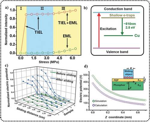
(a) Luminescence intensity of the TIEL/EML in different stress regions as well as the single EML. (b) Energy band structure of the ZnS EL. (c) Changes in surface electric potential of the electrification layer, mapped along the sliding trajectory pre- and post-sliding. (d) Computed and simulated profiles of electric potential across the luminescent layer's thickness. The inset shows the 2D structural diagram. Reproduced with permission from Ref. [115]. Copyright 2016, WILEY-VCH Verlag GmbH & Co. KGaA, Weinheim. EL, electroluminescent; EML, elastico-ML; TIEL, triboelectroluminescence; ZnS, zinc sulfide.
The overall mechanism can be explained as follows: electrons excited by friction fall into shallow electron trap states and then transition to Cu impurity states, resulting in luminescence at a wavelength of 510 nm (Figure 17b). Figure 17c shows that with the onset of sliding, the density of frictional charges on the moving object's surface rapidly reaches a saturation value related to the material. During the early stages of sliding, owing to the accumulation of frictional charges, the surface potential increases considerably, indicating substantial charge transfer at the contacting surfaces. Subsequently, with continued sliding, the surface potential decreases sharply and eventually becomes indistinguishable from the background after sliding 2 cm, indicating that no more frictional charges are formed on the electrified layer. Figure 17d shows the potential along the thickness direction of the luminescent layer underneath the charged sliding object, represented along the z-axis in the inset of Figure 17d.
The ML of ZnS:Mn2+ could also be associated with triboelectric charges. Wang et al. fabricated a triboelectric nanogenerator (TENG) based on ZnS:Mn2+/PDMS.179 They discovered that when the applied pressure was sufficient to induce ML, there was a substantial decrease in both the current and voltage of the TENG, accompanied by a reduction in the triboelectric charges on the PDMS surface. Conversely, when the pressure was too low to generate ML, the triboelectric charges would accumulate without dissipating. Using this TENG to attract foam microspheres, they observed that, compared to specific regions of PDMS composite films without ZnS:Mn2+ phosphors, the ZnS:Mn2+ luminescent layer lost its attraction for foam microspheres after ML, which perhaps suggests that electrical charges contribute to the ML process in ZnS.
Park et al. analyzed the TIEL during the stretching–releasing process of ZnS:Cu/PDMS.166 When ZnS:Cu was combined with PDMS, air entered at the interface, forming natural pores. During the stretching–releasing process, the deformation of PDMS caused the pores to enlarge and then recover (Figure 18a), with friction occurring at the interface between ZnS:Cu and PDMS, causing TIEL. In these experiments, the force was applied indirectly via polytetrafluorethylene (PTFE). The specific ZnS:Cu/PDMS/PTFE structure could generate both internal and external electric fields during the stretching–releasing cycle (Figure 18b,c), enhancing the overall intensity of TIEL. Additionally, the primary reason for choosing PDMS and PTFE as substrates was their ability to generate a higher friction-induced output voltage.
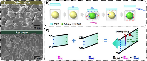
(a) The generation and recovery of pores between ZnS:Cu and PDMS under external forces. (b) Diagrams of the generation of internal and external frictional electric fields during the contact–separation between ZnS:Cu/PDMS and PTFE. When an external force is applied through PTFE, friction charges are generated between ZnS and PDMS, inducing TIEL. When the external force is removed and PTFE separates from PDMS, friction charges are generated, inducing TIEL. (c) Band diagram of the TIEL of ZnS:Cu. The electric field (Einternal + Eexternal) causes band tilting, resulting in electrons in Vs being released and recombining with holes in AlZn, leading to light emission. Reproduced with permission from Ref. [166]. Copyright 2021, American Chemical Society. PDMS, polydimethylsiloxane; PTFE, polytetrafluoroethylene; TIEL, triboelectroluminescence; ZnS, zinc sulfide.
It should be noted that bare exposed ZnS:Cu is less likely to exhibit TIEL, making it necessary to cover the surface of ZnS:Cu with a layer of AlOx. Lee et al. discovered that ML in ZnS:Cu (D512C, bi-phase structure,96 Shanghai Keyan Optoelectronic Technology Co., Ltd.)/PDMS could not be attributed to the frictional electrification between ZnS:Cu and PDMS. Instead, it arose from the frictional electric properties at the PDMS-AlOx interface.109 They compared the effects of coating the surface of ZnS:Cu with AlOx and leaving it uncoated, and found that only the former exhibited an extremely pronounced ML (Figure 19a,b). Based on several common triboelectric materials (Figure 19c), they used wet chemical methods to grow different layers on the surface of bare ZnS:Cu (D512B, Shanghai Keyan Optoelectronic Technology Co., Ltd.), and combined them with two substrates—that is PDMS and polyurethane (PU)—which had similar mechanical properties (elastic constant ≈ 2 MPa) but different frictional electric characteristics. By analyzing the post-friction voltage, current, and charge density (Figure 19d–f), they found that PDMS-AlOx and PDMS-MgO outperformed in all of these parameters, which corresponded to the strong ML evident in ZnS:Cu@AlOx/PDMS and ZnS:Cu@MgO/PDMS (Figure 19g).
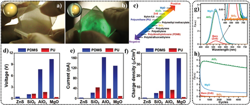
(a, b) TML tests, showing commercial ZnS:Cu microparticles placed between PDMS blocks, without (a) and with (b) Al coating. (c) Assessment of the impact of common triboelectric coating series on the ML of ZnS:Cu/PDMS composites on the surface of ZnS:Cu phosphor. (d–f) Measurement of triboelectric voltage, current, and triboelectric charge density at various oxide-polymer interfaces. (g–h) ML spectra and ML peak intensity attenuation curve (during repeated stretch–release cycles) of ZnS:Cu/PDMS composite films with different types of coating. Reproduced with permission from Ref. [109]. Copyright 2024, Wiley-VCH GmbH. ML, mechanoluminescence; PDMS, polydimethylsiloxane; TML, tribo-ML; ZnS, zinc sulfide.
As mentioned earlier, the luminescence of ZnS:Cu in powder-based ACEL can be attributed to the presence of CuxS conductive needles in the ZnS:Cu phosphor. These needles significantly boost the AC electric field at their tips, allowing powder-based ACEL to operate at low voltages, as low as 106 V · m−1 (which is two orders of magnitude lower than the voltage required for thin-film ACEL), considerably reducing the threshold voltage for ZnS:Cu luminescence.180-182 Consequently, the frictional charges generated at the AlOx-PDMS interface during frictional motion could even induce EL in this context.
Finally, although both AlOx and MgO can serve as outer shells for ZnS:Cu, the mechanical performance of ZnS:Cu@AlOx/PDMS proved to be superior in the experiments. Its ML intensity remained stable even after more than 5000 stretch–release cycles. By contrast, the ML intensity of ZnS:Cu@MgO/PDMS exhibited an 80% decline after 1200–1400 stretch–release cycles (Figure 19h). They attributed this to the incomplete growth of the MgO coating.109
4 SYNTHESIS OF ZnS WITH TUNABLE PHASES, SIZES, AND MORPHOLOGIES
ZnS is not only pivotal in ML but also extensively used in the production of quantum dots (QDs),183 catalysts,184 and EL devices.179 The interdependence of particle size and material properties has led to the development of diverse synthesis techniques, each tailored to produce specific particle sizes, morphologies, and characteristics of the final products.154, 185, 186
For ML characteristics, it is essential to subject the material to high-temperature sintering, often exceeding 1000°C, to form a complete lattice and allow dopants to enter the crystal lattice structure. Moreover, there is often a trade-off between particle size and luminescence intensity, as reducing particle size leads to an increase in surface defects and a larger specific surface area of small particles, resulting in a weaker ML intensity. Typically, the most common synthesis method is the solid-state method,187 which is straightforward, and its products exhibit excellent ML intensity. However, their drawback is that their particle sizes can be relatively large (several micrometers), and their morphology is non-uniform. Another promising synthesis method is the molten salt method,111 which lowers the reaction temperature by adding molten salt, thereby obtaining smaller particle sizes and relatively controllable morphology, while maintaining strong ML intensity.
To obtain nanoscale ML particles, a newly emerging synthesis method is the biomineral-inspired suppressed dissolution approach.188 This method involves the post-processing of micrometer-sized ML particles to detach nanoscale ML particles, with an average size of <100 nm, while retaining their ML intensity. However, these nanoscale particles are stable in solution, making them suitable for applications requiring liquid-state ML. Other methods for obtaining nanoscale ML particles include various wet chemical methods,187 which can reduce particle sizes to several tens of nanometers or a few nanometers, generating various regular morphologies. Nevertheless, although these methods offer the advantages of controllable particle sizes and morphologies, ZnS synthesized through such methods is generally not used for ML but finds application in other fields.183, 184 The absence of strong ML is one of the primary reasons. On the one hand, the high-temperature sintering process is usually not included in these wet-chemical methods, so the ZnS usually does not exhibit ML properties. On the other hand, even if nanoscale ML particles can be obtained through calcination, it can be challenging to apply stress to them for deformation. Moreover, a large number of surface defects on the nanoparticle surface may act as fluorescence quenchers.189 These reasons together lead to decreasing ML performance in ZnS compared to micrometer-sized particles, making its application more difficult. Nonetheless, it is undeniable that preprocessing through wet-chemical methods can reduce the temperature required for high-temperature sintering, making the process more controllable than the solid-state method. Combustion methods are also a classic synthesis approach, where the energy for the reaction comes from the chemical reaction itself, making it relatively energy-efficient. However, there is currently limited research on synthesizing ZnS particles with ML properties using this approach.
Thermal evaporation190 and ultrasonic spray pyrolysis57 are methods used to synthesize relatively uniform ZnS thin films. In the former method, ZnS is heated to a gaseous state before it recondenses to form a thin film, whereas the latter method involves directly heating a mist of ZnS-containing raw materials, resulting in uniform thin films on larger substrates.
Finally, ZnS exists in two structures—that is, WZ- and ZB-phase structures. Control over these phases during synthesis is one of the key prerequisites for studying its properties. The temperature for the phase transition is approximately 1020°C.74 However, when synthesis methods involve a liquid-state, such as the molten salt method,111 or use liquid-state synthesis conditions,191 both phases of ZnS can be synthesized simultaneously under relatively mild conditions.
4.1 Micrometer-scale ZnS crystals
High-temperature solid-state method
This method offers a simple, high-yield process, but its drawbacks include incomplete reactions and high energy consumption.192 For the synthesis of ZnS:Mn2+ crystals, high-purity ZnS and MnCl2 are commonly employed as starting materials. These materials are weighed, ground, thoroughly mixed in an agate mortar, and transferred to a clean alumina crucible. Subsequently, the mixture is then subjected to a N2 flow reaction at high temperatures for 1 h. After the reaction, the product is cooled to room temperature, removed, and rinsed multiple times with deionized (DI) water or anhydrous alcohol to remove impurities.193
For further improvement, the choice of the annealing atmosphere can also be crucial. Wang et al. proposed that introducing oxygen during the synthesis process could enhance luminous efficiency, as the presence of oxygen positively affects the formation of sulfur vacancies in the ZB structure of ZnS, facilitating the introduction of Mn2+ as luminescent centers and shallow impurity energy levels, thereby increasing the electron–hole recombination rate.192 Through experimentation, the optimal oxygen proportion and Mn2+ doping concentration were found to be 1%–20% and 1%–2%, respectively. Liu et al. reported that under a thermal carbon-reduction atmosphere, the ML peak of ZnS:Mn2+ shifted from 585 to 650 nm, resulting in an overall transition to red light emission, and for the samples doped with 3% Mn2+, the PL and ML intensities were 1.76 and 3.23 times higher, respectively, than those observed under a N2 atmosphere.194 Within the ZnS:Mn2+ framework, the distance between the two nearest Zn2+ sites occupied by Mn2+ ions is notably short (3.823 Å), facilitating the formation of exchange-coupled pairs. The introduction of carbon increases the probability of ferromagnetic coupling in Mn2+–Mn2+. In this scenario, the electron spins of the Mn2+–Mn2+ align in parallel, occupying the bonding and antibonding orbitals, respectively. This configuration decreases the energy from the lowest excited state to the ground state, causing the ML emission to red-shift. The optimal concentration of Mn ions in the experiment was 3%, at which the probability of Mn2+–Mn2+ forming in the ZnS matrix was 12%. Moreover, Gan et al. proposed that annealing in a reducing atmosphere could enhance the ML and PL by regulating the concentration of sulfur vacancies (which provided the trapped electrons).89 Through their research, it was evident that for commercial WZ-ZnS:Cu (Osram Sylvania Inc. GG45), annealing at 250°C for 1 h in a pure hydrogen atmosphere (99.9%) could achieve the maximum enhancement.
Moreover, Feng et al. suggested that the pre-ball milling of raw materials could reduce the average particle size, increase the specific surface area, and enhance the reactivity of the raw materials. This method not only lowered the reaction temperature but also increased the content of WZ-ZnS in the product, thereby improving the luminance of both PL and ML (Figure 20a–c).80 After synthesis, when it needs to be compounded with matrices (such as PDMS), nanoparticles can be added to improve the elastic modulus66 or triboelectric properties,109 enhancing the material's strength and sensitivity under low stress conditions. Available nanoparticles include SiO2, Al2O3, ZrO2, In2O3, MgO, and TiO2, among which SiO2, Al2O3, and ZrO2 have shown notably effective results (Figure 20d–f).195
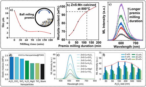
(a) Average particle size of the calcined samples with different milling times. Inset: Preprocessing of the ZnS powder using ball milling. (b) Relationship between the proportion of WZ-ZnS and grinding time (annealing conditions for both are 800°C for 3 h). (c) Relationship between the ML intensity and milling duration. Reproduced with permission from Ref. [80]. Copyright 2023, Elsevier B.V. (d, e) Analysis of the elastic modulus (d) and ML intensity (e) of films incorporating distinct types of oxide nanoparticles (≈100 nm, 10 wt%). (f) Integral ML intensity of films containing Al2O3 nanoparticles of different sizes and content. Reproduced with permission from Ref. [195]. Copyright 2022, Wiley-VCH GmbH. ML, mechanoluminescence; ZnS, zinc sulfide.
Molten salt shielded method
The molten salt shielding method uses molten salts such as NaCl, KCl, and LiCl as a protective layer to synthesize ML materials without the need for costly inert gases.85, 111 In comparison to solid-state method, this method produces powder with a controlled morphology and a uniform particle size. Consequently, it interfaces more closely with polymer composites, enhancing the stability and durability of flexible ML devices.26, 84, 85, 111 Moreover, the inclusion of molten salt promotes better mixing of reactants and isolates the reaction from the surrounding air, which results in lower reaction temperatures and reduced experimental costs while maintaining the material's luminescent brightness. It is important to note that if gas is generated during the reaction, it can disrupt and compromise the sealing integrity of the molten salt layer, excluding gas-forming reactants from the reaction. Additionally, owing to the boiling point of salt, reaction temperatures should not exceed a certain threshold.
A specific procedure for the synthesis of homojunction ZnS:Mn2+ is shown in Figure 21a,111 where the molten salt also serves as a dispersing medium for Mn2+, a reaction medium for ZnS crystal growth, and a diffusion medium for Mn2+ doping into ZnS crystals. Raw materials and salt were mixed together, and another layer of salt was applied to the surface (Figure 21b,c). Owing to the considerable difference in density between ZnS (4.102 g · cm−³) and NaCl (2.165 g · cm−³), and the lower melting point of ZnS (approximately 680°C) compared to NaCl (approximately 804°C) (Figure 21d), ZnS is deposited at the bottom during the reaction. The molten salt on the surface effectively isolates the air (Figure 21e–g). Lastly, the product was washed with deionized water to remove the salt.
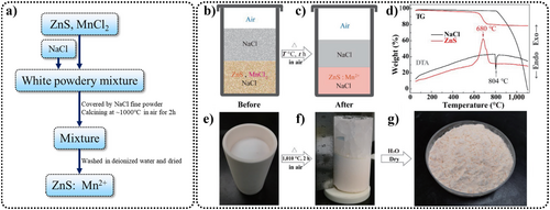
(a) Flowchart of the molten salt shielding method. (b, c) Material partition placement diagram, before (b) and after (c) reaction at high T °C for t h. (d) Thermal characterization of NaCl and ZnS raw materials conducted using a heating rate of 10°C · min−1. (e–g) Images from the actual synthesis process: (e) Loading of the samples, (f) the mixture of salt and phosphor after sintering, and (g) the final ZnS:Mn2+ phosphor product. Reproduced with permission from Ref. [111]. Copyright 2022, Tsinghua University Press. ZnS, zinc sulfide.
4.2 Nano to micrometer-scale ZnS crystals
Wet-chemical methods
Wet-chemical methods encompass various techniques involving liquid-state reactions for material synthesis, such as the sol-gel, hydrothermal, solvothermal, and chemical co-precipitation196 methods. These methods can all be employed for the synthesis of ZnS nanoparticles, which has application in areas such as QD luminescent materials,197-200 catalysis,201 antibacterial purposes,202 and solar cells,203, 204 among others. To impart ML properties to the material, the final step often involves high-temperature sintering.
The sol-gel method is a technique that involves hydrolysis and polymerization reactions of raw materials in a liquid-state, resulting in the formation of a gel that can then be dried to obtain the desired product. This method allows for uniform and controlled doping, with relatively low reaction temperatures and has been employed to synthesize (ZnS)1-x(MnTe)x,205, 206 ZnS:Mn2+,207 and ZnS:Cu,208 among others. However, the drawbacks include higher raw material costs, as some materials are strong acids, strong bases, or organic compounds harmful to both human health and the environment. Experimentally, it also involves complex and relatively time-consuming steps.209 Differing from the atmospheric conditions of the sol-gel method, the hydrothermal method employs a high-pressure stainless steel reaction vessel as the reaction container. This method involves promoting the recrystallization or reaction of substances in a solvent under medium- to high-pressure conditions and at a particular temperature. A specific procedure is shown in Figure 22a.210 When a material cannot be prepared in water, alternative solvents are commonly employed, based on the solvothermal synthesis method.191 While sharing similarities with the hydrothermal method, the solvothermal synthesis method offers the advantage of enabling control over the phase type of ZnS by varying the solvent type.191
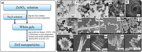
(a) Flowchart of the hydrothermal method. (b–f) Morphologies of ZnS synthesized using the hydrothermal method. Among them, (b–d) are TEM images of nano-sized ZnS with different sizes after adjusting the Zn2+:S2− ratios (1:0.7, 1:1, 1:1.3). Reproduced with permission from Ref. [210]. Copyright 2009, IOP Publishing Ltd. (e, f) are hierarchical flower-like ZnS (En)0.5 white precipitate. Reproduced with permission from Ref. [60]. Copyright 2013 Elsevier B.V. (g–o) Morphologies of ZnS synthesized using the solvothermal method. Among them, (g–j) are TEM and SEM images of ZnS nanocrystals synthesized under different conditions (220, 160, 180, and 200°C) with an inset in (g) showing an HRTEM image at the edge of a sphere. (k–o) Details of the morphological evolution of ZnS crystals by adjusting the HNO3 content in the mixed solvent (0.1, 0.3, 0.6, 0.8, and 1.2 mL). Reproduced with permission from Ref. [191]. Copyright 2008, American Chemical Society. HRTEM, high-resolution transmission electron microscope; SEM, scanning electron microscope; TEM, transmission electron microscopy; ZnS, zinc sulfide.
These methods are suitable for controlling the size and morphology of ZnS nanoparticles. For instance, Tran et al. achieved particle-size variation by adjusting the molar ratio of Zn2+ to S2- (Figure 22b–d).210 Zhao et al. transformed the particle morphology between microspheres, urchin-like structures, and hierarchical flower-like superstructures by controlling the ratio of ethylenediamine (En)—a chelating agent capable of forming complexes with Zn2+/Mn2+—to distilled water and reaction time (Figure 22e,f).60 Jiang et al. induced changes in the size (200, 350, up to 450 nm) (Figure 22g–j) and morphology (spheres, rods, microflowers, and biphasic structures) (Figure 22k–o) of ZnS by altering the solvents (ethylene glycol, ethylenediamine, and hexanol), modifying the reaction temperature, and adding HNO3, among other conditions.191
The heating process can also take the form of microwave-assisted methods.211 Compared to infrared waves, microwaves have longer wavelengths, resulting in greater penetration ability. This allows for instantaneous and uniform heating of the entire reaction volume, ensuring rapid heating. Moreover, microwave heating eliminates the problem of the actual temperature lagging behind the set temperature, providing more precise temperature control. The microwave-assisted method can be advantageous for synthesizing well-dispersed nanomaterials as microwaves induce molecular collisions and friction among materials, preventing agglomeration.212, 213 This method has been employed to synthesize ZB-ZnS nanorods,211 ZnS nanoparticles doped with ions such as Ag+, Cu2+, Ce3+, and Sn4+,214, 215 as well as ZnS QDs.213
The one-pot method is conceptually similar to the sol-gel method, and can be used to synthesize ZB-phase ZnS QDs or nanocrystals.183, 216 A typical procedure for this method is shown in Figure 23a,b, where gelatin plays an essential role as a capping agent, effectively controlling the growth of nanoparticles to maintain colloidal stability and prevent uncontrolled aggregation, ultimately leading to the formation of smaller nanoparticle nuclei.183 The addition of gelatin also enables the composite to transition between a solid-state and liquid-state in response to external temperature changes (Figure 23c,d). The liquid ZnS QDs/gelatin nanocomposite can be used for fluorescence labeling and bioimaging (Figure 23c). Other substances can also serve as capping agents. In the study conducted by Zhang et al.,217 1-dodecanethiol was employed, which forms strong bonds with the surface atoms of semiconductor nanocrystals. Consequently, thiol ligands can render Mn2+ much less reactive, thereby aiding in the formation of stable, small-sized ZnS core nanoclusters.217 Even with an experimental heating time of up to 1 h, the particle size of the product remained <2 nm, with a quantum yield (QY) of 65% (Figure 23f,g). In the research of Zhang et al.,218 Cu:Zn-In-S/ZnS QDs synthesized using the one-pot method exhibited a high PL QY of up to 85%. Additionally, they could adjust the emission color by varying the In/Zn precursor ratio and Cu ion concentration (Figure 23h,i).218
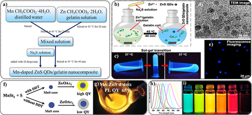
(a) Flowchart of the one-pot method. (b) Diagram showing the experimental procedure for the one-pot synthesis of ZnS QD/gelatin nanocomposite. (c) Vial inversion test to assess the sol-gel transition in the ZnS QD/gelatin nanocomposite. (d) TEM image of the ZnS QD/gelatin nanocomposite. (e) Fluorescence microscopy image of Staphylococcus aureus after incubation with the ZnS QD/gelatin nanocomposite (37°C, 24 h). Reproduced with permission from Ref. [183]. Copyright 2020, American Chemical Society. (f) Synthesis of ZnS:Mn2+ nanocrystals. (g) Photograph of ZnS:Mn2+ QDs under irradiation using a UV light. Reproduced with permission from Ref. [217]. 2011, American Chemical Society. (h) Normalized PL emission spectra (λex = 350 nm) of Cu:Zn-In-S/ZnS QDs under different In/Zn precursor ratios and Cu ion concentrations; (i) Photograph of samples under the radiation of a UV light. Reproduced with permission from Ref. [218]. Copyright 2014, American Chemical Society. QDs, quantum dots; ZnS, zinc sulfide.
Biomineral-inspired suppressed dissolution approach
The biomineral-inspired suppressed dissolution approach is a unique method that draws inspiration from the demineralization processes of bone and enamel (Figure 24a,b).65, 188 Through analysis of the Gibbs free energy, it is known that minerals and ceramic materials exhibit a critical size in solution, below which they do not undergo dissolution. For most ceramic materials, this critical size ranges from 10 to 100 nm. ML materials can be considered a type of ceramic material, and most ML particles prepared through high-temperature solid-state methods are in the micrometer range, far exceeding the critical size of 10–100 nm. Consequently, spontaneous dissolution occurs in the solution, releasing nanocrystals. However, owing to high surface tension, these particles tend to spontaneously precipitate. This problem can be addressed using an undersaturated solution of citrate, which (with its lower pH), accelerates the dissolution process. The negative charge provided by citrate decomposition can stabilize ML nanocrystals, forming a colloidal solution. This approach initially requires the synthesis of micrometer-sized ML particles through conventional methods such as solid-state reactions. These particles can then be subjected to ball milling, before partially dissolving them in a solution. Unlike ball milling throughout the entire process, this method avoids problems related to luminescence quenching resulting from excessive stress and dislocations.188
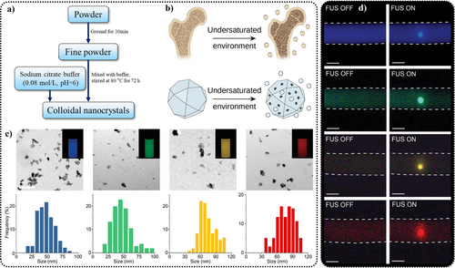
(a, b) Flowchart of the suppressed dissolution approach and its source of inspiration: the kinetically preserved dissolution mechanism of natural biominerals. (c) TEM images of various nanometer-sized particles synthesized through the suppressed dissolution approach, along with their corresponding fluorescence images in aqueous solution (insets) and particle size distribution. From left to right, these particles are Sr2MgSi2O7:Eu2+/Dy3+, ZnS:Cu/Al3+, ZnS:Mn2+, and CaTiO3:Pr3+. (d) Luminescent images of the four materials in (c), with the FUS turned off and on. Reproduced with permission from Ref. [188]. Copyright 2022, American Chemical Society. FUS, focused ultrasound; TEM, transmission electron microscopy; ZnS, zinc sulfide.
The synthesis of ZnS:Mn2+ nanoparticles is shown in Figure 24a,b. It efficiently yields water-soluble ML nanocrystals with diameters as small as 20 nm (Figure 24c), while retaining the strong ML emission synthesized using high-temperature solid-state methods. Additionally, these ML liquids can be recharged with UV light and excited with focused ultrasound (FUS) (Figure 24d). These characteristics contribute to deep tissue imaging and optogenetics achieved by intravenous injection of ML nanocrystals using FUS. Apart from ZnS, this method can also be applied to waterproof materials such as Sr2MgSi2O7:Eu2+/Dy3+, and CaTiO3:Pr3+. However, for some ML materials that react with water (such as SrAl2O4), process modifications may be necessary.188
Combustion method
As a classical chemical synthesis method, the combustion method has been widely employed to synthesize hundreds of compounds, including ZnS nanocrystals and QDs, owing to its advantages such as energy efficiency, simplicity of operation, low cost, and high product reactivity.219, 220 The energy required for combustion reactions is derived from the reactions themselves, with heat propagating in the form of a combustion wave from the reaction zone to other regions, inducing reactions between different compounds. However, for reactions that cannot sustain themselves, chemical furnaces or preheating methods can be applied to prevent interruptions during the reaction. A specific procedure is shown in Figure 25a, where the particle size of the product can be adjusted by varying the oxidizer and fuel ratio (O:F) (Figure 25b).219 However, it is worth noting that the combustion method may produce toxic gases during the synthesis process, which can pose an environmental burden.

(a) Flowchart of the combustion method. (b) Particle size distribution of ZnO/ZnS nanoparticles synthesized with O:F ratios of 1:1 and 2:3. Reproduced with permission from Ref. [219]. Copyright 2019, Springer Science Business Media, LLC, part of Springer Nature. ZnS, zinc sulfide.
4.3 Thin films and nanostructures
Thermal evaporation deposition
Thermal evaporation deposition is a process in which a material is heated to the point of evaporation, and the evaporated atoms or molecules condense onto a substrate to form a thin film (Figure 26a). Thin films of ZnS are more susceptible to stress and can be easily sprayed or adhered to target objects, enabling efficient mechanical-to-optical energy conversion.66, 221, 222 Moreover, this method can also be used to efficiently prepare ZnS of various morphologies, such as nanowires, nanobelts, nanorods,58 thin films, and even pyramid shapes (Figure 26b–e).59 The raw material used is ZnS, and the heating source can be a tube furnace,59, 190 or laser,223 etc. The heating atmosphere can be selected as NH3 or Ar, and the substrate can be made of quartz,59 Si,190 GaAs,58 optical glass, steel, aluminum oxide, silicon nitride ceramics,224 or piezoelectric materials,95 among others. During the preparation process, catalysts such as Au, Sn, and Bi can be added to the substrate or raw materials to assist in nucleation.225 Currently, the application of thermal-deposition synthesized ZnS thin films and nanowires is focused primarily on areas such as nanofriction generators and electronic sensors.226-228
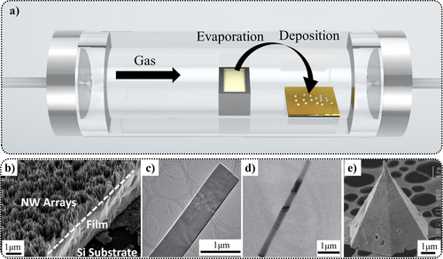
(a) Thermal evaporation deposition experimental apparatus. (b–d) Different nanostructures of ZnS:Nanowire arrays (b). Reproduced with permission from Ref. [190]. Copyright 2009, American Chemical Society; Nanobelts (c); Nanorods (d). Reproduced with permission from Ref. [58]. Copyright 2013, WILEY-VCH Verlag GmbH; Pyramid shape (e). Reproduced with permission from Ref. [59]. Copyright 2009 WILEY-VCH Verlag GmbH & Co. KGaA, Weinheim. SEM images for (b, e), TEM images for (c, d). SEM, scanning electron microscope; TEM, transmission electron microscopy; ZnS, zinc sulfide.
Using the process of synthesizing array-type one-dimensional ZnO-ZnS nanowires by Lu et al. as an example,190 first, 1 g ZnS powder was placed in an alumina boat and positioned at the center of a tube furnace. Then, a silicon wafer coated with a 15-nm Au film (as nucleation sites to facilitate the formation of continuous films) was used as the substrate. After evacuating to a 100 mTorr vacuum, high-purity Ar gas was fed into the system at a flow rate of 50 sccm, maintaining the pressure within the tube at 5 Torr during the synthesis. Subsequently, the tube furnace was heated to 800°C, increasing the temperature at a rate of 50°C · min−1, held for 10 min, before being further heated to 1100°C at a rate of 20°C · min−1, followed by a 60-min holding period, before finally being allowed to cool naturally. Owing to residual oxygen during the synthesis process, ZnO continues to grow at the end of the ZnS nanowires, forming ZnO-ZnS heterostructures, while pure ZnS nanowires can be obtained through selective etching.190
Similarly, materials can also be evaporated to form thin films using an electron beam.224 Xu et al. deposited ZnS films on different substrates using this method and achieved a twofold enhancement in ML intensity by adjusting the growth process parameters.224 The orientation and surface morphology of ZnS films can be further controlled through vacuum annealing processes (500–700°C), enhancing the adhesion between the film and the substrate, thereby improving the piezoelectric field energy conversion efficiency.23, 229-231 To overcome the problem of ZnS film detachment during ML testing, a ZnO buffer layer can be added between the ZnS film and the substrate.231
Ultrasonic spray pyrolysis
Ultrasonic spray pyrolysis is a technique for synthesizing nano-sized crystals or producing thin-film materials. It has been employed in the preparation of metal sulfide nanoparticles,232 carbon nanocapsules,233 metal oxide ML particles,234 ZnS films235, 236 and nanoparticles (ZnS:Ni2+,57 and ZnS:Eu3+ 237, 238), among others. In this method, precursor solutions are atomized using an ultrasonic frequency nebulizer, resulting in a fine vaporized mist that facilitates the formation of extremely-thin-film layers. The size of the droplets in the spray jet decreases as the nebulizer's frequency increases, enabling adjustment of droplet size through frequency modification.
Using the synthesis setup shown in Figure 27 as an example,57 the process begins with the use of a high-frequency ultrasonic spray system to atomize a precursor solution (prepared by dissolving ZnNO3, CH4N2S (thiourea), NiNO3, and colloidal silica aqueous solution in a stoichiometric ratio). Subsequently, an inert gas (Ar) is employed to transport the atomized droplets into a high-temperature furnace for a reaction at 700°C. As the water rapidly evaporates, due to the limited solubility of ZnS and its precursors, the droplets decompose and form an outer shell rich in ZnS, with the inner core comprising primarily silica particles. The silica particles can be dissolved in hydrofluoric acid (HF) ethanol solution, resulting in the formation of nanostructured WZ-ZnS:Ni2+ hollow microspheres (as shown in Figure 27b,c). It is important to note that when the furnace temperature increases from 700 to 1000°C, the final product (after HF treatment), comprises aggregated nano-sized particles with the microspheres losing their structural integrity, as shown in Figure 27d,e.57 In a control experiment, when the same precursor solution devoid of colloidal silica is processed in a tube furnace at 1000°C with an Ar gas flow, only micrometer-sized ZnS:Ni2+ solid microspheres are produced, as depicted in Figure 27f,g.57
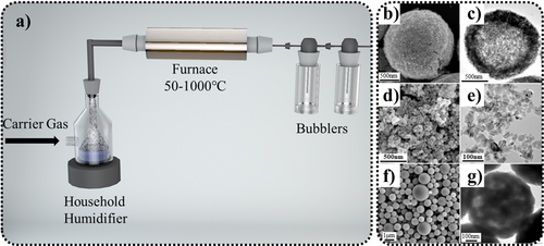
(a) Ultrasonic spray pyrolysis experimental apparatus. (b–g) SEM and TEM images of nanostructured ZnS:Ni2+:hollow microspheres (b, c), nanoparticles (d, e), and non-templated solid microspheres (f, g). Reproduced with permission from Ref. [57]. Copyright 2008, WILEY-VCH Verlag GmbH & Co. KGaA, Weinheim. SEM, scanning electron microscope; TEM, transmission electron microscopy; ZnS, zinc sulfide.
Although this method has advantages (such as the low consumption of raw materials and low reaction temperatures), controlling the thermal treatment process of atomized droplets within high-temperature furnaces can be challenging, and the quantity synthesized in a single run is relatively small. Consequently, it is still necessary to improve the overall process.
5 ML MEASUREMENT METHOD
The testing schemes for ML are diverse but can be broadly categorized into three parts—that is, signal generation, signal transmission, and signal capture, as shown in Figure 28. The ML signal can be obtained through various means such as friction,230, 239 deformation,240 impact,241 and ultrasound.242, 243 Weak stress can be implemented using an atomic force microscopy (AFM) probe244 while strong stresses can be applied using a diamond anvil.34, 78
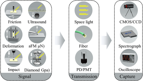
Methods for ML measurement, including the generation, transmission, and capture of ML signals. ML, mechanoluminescence.
The transmission process can be categorized based on the medium, including direct propagation in space (Space light), propagation in a medium (Fiber), and conversion into electrical signals through a photoelectric detector (PD) or photomultiplier tube (PMT). At the signal capture end, the main options include a complementary metal-oxide-semiconductor (CMOS)/charge-coupled device (CCD), spectrograph, and oscilloscope.
5.1 Impact testing method
The impact testing method has been widely used to test ML signals. It involves the direct impact of a steel ball or other objects on ML materials, the collection and quantification of the ML signal and its intensity. It has the advantages of simplicity, high repeatability, and low cost. However, it can pose challenges when testing liquid samples. Additionally, signal collection typically occurs only once per impact, resulting in a relatively short contact time between the sample and the steel ball and a weaker ML signal.
In a setup used by Fontenot et al., a pin acted as a switch to control the free fall of a steel ball, which impacted a plexiglass plate evenly coated with ML powder.241 The emitted light from this impact was collected using a PD positioned below the glass plate (Figure 29a). Similarly, the scheme developed by Lin et al. exhibited greater precision and compactness (Figure 29b).29 They used an electromagnet as a switch to control the free fall of the steel ball. The ML powder was mixed with PMMA and encapsulated in polyvinyl chloride (PVC) as a film to prevent measurement errors caused by the movement of the powder during the impact. The emitted light was then collected using a CMOS sensor located below the glass plate.
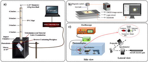
Impact testing systems. (a, b) Experimental setup with a pin (a) or magnetic switch (b) to control the falling of the ball. Reproduced with permission from Ref. [241]. Copyright 2011, Elsevier Ltd. Reproduced with permission from Ref. [29]. Copyright 2022, American Chemical Society. (c) Experimental setup based on a high-speed spherical projectile. Reproduced with permission from Ref. [245]. Copyright 2022, The Author(s). Published by Elsevier Ltd.
For scenarios involving high speeds and large impact forces, additional devices are needed to impart kinetic energy to the impacting ball. Haider et al. used an airsoft electric gun to accelerate the ball to speeds of several tens of m · s−1 (Figure 29c).245 Other components of the system included a speedometer, target cylinder, condenser followed by an optical fiber, PMT, and digital oscilloscope. The airsoft electric gun imparted kinetic energy to the ball, shooting it toward the target material film from a distance of 20 cm. The PMT captured photons through optical concentrators and fiber optics, with the oscilloscope recording the light intensity. The optimized system reduced the lateral area and allowed for easy adjustment of the projectile's mass to regulate the mechanical energy. More powerful acceleration devices could achieve higher speeds, as demonstrated by Bergeron et al., who used a two-stage ultra-high-speed light gas gun to accelerate the ball to 5–6 km · s−1,246 and Fontenot et al., who achieved a speed of 410 ± 9 m · s−1 with their setup.247
5.2 Friction, deformation and ultrasonic testing method
Owing to the fact that a multitude of ML materials exhibit TML rather than DML, frictional methods are often used to obtain ML signals. Typically, prior to testing, samples require a degree of preprocessing, with samples prepared as films either directly encapsulated or mixed with a matrix to prevent powder movement during loading. Subsequently, a mechanical device applies a certain frequency of friction to the sample, and the ML signal is collected and analyzed through the PMT or CMOS devices.
Using the setup by Peng et al. as an example, the material was reciprocally rubbed in the horizontal direction to generate ML, as shown in Figure 30a.33 In this testing system, the ML powder, mixed with ultraviolet-curable adhesive, was encapsulated as a film and affixed to a transparent quartz plate to secure the sample. A metal probe with adjustable pressure served as the force applicator. Friction was controlled using a programmable linear motor to regulate both the distance and frequency of friction. The resulting ML signal was captured using a fiber optic probe through the quartz plate and transmitted to the spectrometer for subsequent data collection.
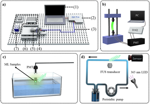
ML measuring system, based on friction (a), deformation (b) and FUS (c, d). In (a), the sample undergoes friction, generating an ML signal, which is then analyzed using a spectrometer and transmitted to the computer. This system includes (1) a computer, (2) fiber optic spectrometer (Ocean Optics QE65Pro), (3) fiber, (4) transparent quartz plate (to fix the sample), (5) digital push–pull gauge, (6) three-dimensional displacement platform, (7) and linear motor. Reproduced with permission from Ref. [33]. Copyright 2020, WILEY-VCH Verlag GmbH & Co. KGaA, Weinheim. In (b), the sample undergoes deformation, generating an ML signal, which is then transmitted to a computer using a PMT and DAQ device. Reproduced with permission from Ref. [240]. Copyright 2018, Elsevier Ltd. In (c), the sample undergoes ultrasonic stimulus, generating an ML signal, which is then collected using a PMT. Reproduced with permission from Ref. [242]. Copyright 2012, Elsevier B.V. In (d), a peristaltic pump enables the solution to be cyclically charged and discharged, making it suitable for repeated testing. Reproduced with permission from Ref. [243]. Copyright 2023, Springer Nature Limited. DAQ, data acquisition; FUS, focused ultrasound; ML, mechanoluminescence; PMT, photomultiplier tube.
Deformation methods include tensile and compression deformation tests, differing primarily in the direction of the applied force on the sample. Specifically, sample preprocessing is also required to prepare samples as thin films or coat them onto external deformable substrates. The samples are then subjected to tensile or compression forces using a linear displacement platform or a loading machine. In the testing conducted by Shohag et al. (Figure 30b),240 an 858 MTS testing machine was employed, with a mechanical force dynamically applied in the vertical direction. The ML signals were amplified using a PMT before entering a data acquisition device, with a computer program converting the output voltage into digital signals.
In cases where the ML material is liquid, forces cannot be directly applied; consequently, an indirect method of application through ultrasound can be used. In the apparatus used by Terasaki et al.,242 the ML particles combined with an adhesion matrix were fixed at the bottom of a sample tube, and ML was excited in an ultrasonic cleaning bath, with light being collected using a PMT and photon counter (Figure 30c). Moreover, the testing apparatus by Jiang et al. exhibited a higher degree of automation.243 They constructed a circulatory system with a peristaltic pump serving as the power source (Figure 30d). At one end of the system, a UV light charged the ML colloidal solution, and at the other end, a FUS transducer excited the ML, with the light being transmitted to a spectrometer for detection. The ML colloidal solution was then recirculated back to the charging end by the peristaltic pump, with the entire process being controlled by software (such as LabVIEW and MATLAB), facilitating cyclical testing.
5.3 Extreme condition testing method
In the case of extremely small or exceedingly large stresses, special equipment is required for testing. An AFM probe can be used for the observation of ML at the particle level, but its complexity and high cost are drawbacks.244 Nonetheless, it enables the observation of ML processes at the microscopic level and allows for the visualization of particle fracture after force application.
Sakai et al. used this method to investigate ML emissions from SrAl2O4 particles under conditions of elastic deformation, friction, and destructive deformation.244 They employed a cantilever with 10-nm tip radius as the force applicator, varying the applied force by adjusting the magnitude of the deflection voltage (Figure 31a). Additionally, owing to molecular forces, when the cantilever approached the ML particles, it would suddenly draw closer, leading to a sudden change in the actual applied pressure at that moment. Consequently, the experimental setup also incorporated laser deflection methods to measure the deformation of the AFM cantilever, providing data on the force during these abrupt changes. The stress applied using this method could be as low as the μN level. However, owing to the minimal number of photons collected (approximately a few hundred), the PMT was necessary to amplify the signal, although this method exhibited a relatively low signal-to-noise ratio, requiring multiple measurements.
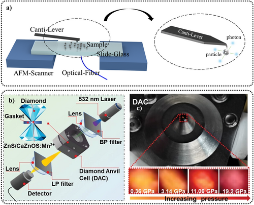
(a) ML measuring system based on AFM. The system comprises an AFM and photon counting system. Reproduced with permission from Ref. [244]. Copyright 2006, Royal Society of Chemistry. (b) ML measuring system based on a DAC. The system comprises a light source, filters (band pass and long pass), DAC, lens, and detector. (c) PL photographs taken under UV irradiation in a DAC at specified pressures. Reproduced with permission from Ref. [34]. Copyright 2023, The Authors. Advanced Materials published by Wiley-VCH GmbH. AFM, atomic force microscopy; DAC, diamond anvil cell; ML, mechanoluminescence.
High-pressure testing can be achieved by applying extreme pressure using exceptionally hard materials, such as diamond.34, 78 In the apparatus developed by Zheng et al.,34 a 532-nm laser served as the excitation source, and a diamond anvil cell (DAC) was employed as the pressure application end for ML testing, with a maximum pressure reaching 19.20 GPa. The samples were mixed with micrometer-sized rubies and loaded into the DAC chamber, while the pressure during PL testing was transmitted through a pressure transmitting medium (a mixture of methanol/ethanol/water). The generated ML signal was collected using a CCD after having passed through a long-pass filter and lens, as shown in Figure 31b,c.
6 APPLICATIONS AND DEVICES
Compared to traditional stress sensors based on optical or electrical principles, ZnS ML-based stress sensors offer unique characteristics such as wireless sensing, flexibility, surface sensing, and a linear response. They can emit light directly under mechanical actions such as stretching, friction, and pressing, making them suitable for a wide range of applications. Dispersed ZnS powder can be difficult to subject to stress because it tends to move in all directions under external forces. Consequently, it should be combined with organic high-polymer compounds to prepare flexible composite films, where the compounds transmit force to the ZnS particles.248, 249 The available compounds include PDMS,63, 250, 251 PU,252, 253 PVDF,97, 254 PVC,255 polystyrene,256, 257 polyester resin,258 and organic hydrogel materials.259
The flexible-film manufacturing process is relatively straightforward, involving the uniform mixing and solidification of the compound with ZnS crystals. However, the sensor films manufactured using this method are primarily sensitive to mechanical changes such as stretching and friction. To achieve multimodal and higher-precision sensing functions, multi-layer composite films are required. Typically, a “sandwich” structure is adopted, comprising a protective layer, functional layer, luminescent layer, and substrate. Some sandwich-structured films are also equipped with data lines and conductors for data processing and transmission.115, 260 In multi-layer structures, the protective layer not only needs to exhibit a certain degree of friction resistance but also has good transparency. The role of the functional layer can be adjusted according to specific requirements. On the one hand, it can convert external mechanical forces into an electric field,115 to excite and enhance the ML of the luminescent layer. On the other hand, it can connect the protective layer and luminescent layer, providing a fixation function.25 In some structures, it can also enhance the conductivity and performance of the luminescent layer.261 The luminescent layer comprises ZnS crystal powder combined with a high polymer and serves to transform energy into light emission. The substrate should exhibit good adhesion and transparency, providing support and protection for the other layers.262
ZnS ML devices with composites can be used in various applications, including electronic bioimaging, electronic signatures, anti-counterfeiting, flexible wearable devices, strain sensing, energy-saving displays, and multimode responsive devices. In this section, we will introduce these applications and analyze their characteristics.
6.1 E-signature and anti-counterfeiting applications
Signatures are considered an effective anti-counterfeiting technology, with the main principle being authentication based on individual signing habits and characteristics.263 Consequently, ZnS-based electronic signature and anti-counterfeiting systems represent a category of anti-counterfeiting solutions. Compared to traditional electronic solutions, they offer the advantages of being passive and having simple structures, resulting in longer lifespans. One of their key advantages is the real-time recording of the signer's signing habits, which can render the signature more difficult to forge. Even in extreme environments (such as prolonged exposure to humidity), these sensors can maintain high response speeds and sensitivity.97, 264
The spatial resolution of an ML anti-counterfeiting system depends on the micro-patterning technology used during manufacturing. Wang et al. used a standard photolithography process to fabricate large-scale ZnS ML photoresist arrays on a polyethylene terephthalate substrate, achieving a high spatial resolution of handwritten fonts up to 100 μm (254 dpi) (Figure 32a,b).25 Additionally, it is possible to enhance the resolution by creating molds with unit cells through photolithography and filling them with ML powder. This fabrication method offers the advantages of avoiding crosstalk between adjacent units and mitigating any adverse effects that can result from the direct mixing of ML powder and photoresist (Figure 32c–e).115, 260 Moreover, they developed an ML signature anti-counterfeiting system capable of visualizing handwritten signatures (Figure 32f–h). This system enabled single-point dynamic pressure recording and 2D planar pressure mapping within the range of 0.6–50 MPa, achieving rapid response times of <10 ms.25
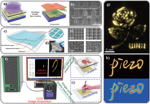
(a) Schematic illustration of the UV photolithography fabrication process of ML arrays. (b) SEM images of array-structured. Reproduced with permission from Ref. [25]. Copyright 2015, WILEY-VCH Verlag GmbH & Co. KGaA, Weinheim. (c) Schematic illustration of the structure of the luminescent layer. (d) Photograph of a twisted composite material. (e) SEM images of the empty cells made from graphite-doped PDMS, and cells filled with phosphor particles, left: top-down view, right: tilted view at 45° angle. Reproduced with permission from Ref. [115]. Copyright 2016, WILEY-VCH Verlag GmbH & Co. KGaA, Weinheim. (f) Schematic illustration of the image acquisition and processing system, which can record the ML signal from (i) planar pressure and (ii) single-point dynamic pressure. (g, h) ML signal of a stamp and a signing process with its stress distribution. Reproduced with permission from Ref. [25]. Copyright 2015, WILEY-VCH Verlag GmbH & Co. KGaA, Weinheim. ML, mechanoluminescence; PDMS, polydimethylsiloxane; SEM, scanning electron microscope.
ACEL devices based on ZnS can also be used for signature and anti-counterfeiting systems. Moreover, such devices can effectively prevent triplet-triplet or triplet-charge annihilation, which occurs in traditional direct current injection-driven devices at high charge densities.265 This is because the continuous flipping of the applied electric field can prevent electron accumulation. Ji et al. demonstrated a new three-phase electric-power-driven EL (TPEL) device structure, that could be easily integrated into 110/220 V and 50/60 Hz AC power systems, considerably improving system integration.265 These TPEL devices can be thought of as three parallel capacitors, each phase being 120° out of phase with the others. When a polar electrode bridge (such as a water layer) is attached to the top of the luminescent powder layer, these capacitors become a series of connected capacitors, with the luminescent powder layer sandwiched between the electrodes and polar electrode bridge. During AC excitation, the direction of the dipole moment above the polar electrode bridge continuously flips, inducing an electric field perpendicular to the luminescent powder layer and resulting in EL. Researchers have demonstrated a lollipop-shaped electrode pattern (Figure 33a), which can be written on with water, recording the writer's handwriting. It does not require complex back circuits and pressure sensors, and the marks can be restored to their initial state through drying (Figure 33b,c).265 Zhu et al. developed a flexible self-powered patterned EL device based on TENGs to overcome the problem of traditional QR codes being invisible in the dark. The device comprised a ZnS:Cu/PVDF-HFP composite material (light-emitting layer), flexible upper indium tin oxide electrodes, and patterned lower laser-induced copper electrodes. It generated electricity through friction from the TENGs, enabling custom pattern display and visual information interaction (Figure 33d).266

Visualization of dynamic pressure distribution. (a) Photograph of lollipop-shaped electrodes for TPEL panels. (b) Photograph of a rewritable interactive display being written upon using DI water (as the polar bridge). (c) When water is on the TPEL panel, the area glows, which can be used as an optical alarm outdoors. Reproduced with permission from Ref. [265]. Copyright 2021, The Author(s). (d) Schematic illustration of information interaction based on the QR-EL system. Reproduced with permission from Ref. [266]. Copyright 2022, Elsevier Ltd. (e–h) Illustration of information being written on a ZnS:Cu/PDMS film: (e) information record; (f) photograph of the film under sunlight; (g, h) when excited by ultrasound, the corresponding luminescence photograph and its intensity distribution. (i–k) The encoded data becomes visible in the dark when excited by ultrasound. Reproduced with permission from Ref. [267]. Copyright 2019, Royal Society of Chemistry. (l) SEM images of the dried pulp mixture of wood fibers and ML powder, with an inset showing the fluorescent microscope image. (m, n) ML effect when the ML paper is scraped and cut with scissors. (o–q) ML labels under natural light (o), illuminated by a 365-nm UV lamp (p), and subjected to friction using a finger (q). Reproduced with permission from Ref. [111]. Copyright 2022, Tsinghua University Press. (r) Signal conversion process for ML fingerprint unlocking. Reproduced with permission from Ref. [268]. Copyright 2023, American Chemical Society. DI, deionized; ML, mechanoluminescence; PDMS, polydimethylsiloxane; TPEL, three-phase electric-power-driven electroluminescent; ZnS, zinc sulfide.
Usually, ML signature anti-counterfeiting systems rely on capturing ML using an image acquisition unit and analyzing it using custom software, lacking the capability to store information. To address this challenge, Zuo et al. proposed a solution by applying force to specific areas of an ML film in advance and then exposing the film to other mechanical stimuli, which triggered visible light emission to reproduce the information (Figure 33e–k).267 This was because the microstrain in the prestressed area was invisible when the external force was removed, becoming visible only when subjected to external mechanical forces (such as stretching, wind, and ultrasound)—that is, this device could accurately remember the locations where it experienced stress and invisibly store these changes, which could then be reproduced as visible light through opening/closing external stimuli.267 Water mist could also reproduce information stored in the film, without the need for additional equipment or power units, making the entire system compact. This was due to the static charge generated from friction between the water droplets and substrate material, stimulating ZnS material to emit friction-induced luminescence.269-271
Aside from electronic signatures, ML ink and paper also have enormous potential in anti-counterfeiting applications. Ma et al. prepared ML paper by mixing ZnS:Mn2+ ML powder with pulp, which could have patterns directly printed on it (such as floral patterns) using a commercial laser printer (Figure 33l–n).111 Under a fluorescence microscope, these ML particles emitted yellow light. Owing to the partial penetration of ML from internal particles, they exhibited an enhanced luminescence response to external stress. Self-adhesive label stickers made from the ML paper were white but turned yellow under a UV lamp (Figure 33o,p), emitting bright yellow light under the friction of a finger (Figure 33q), demonstrating sensitivity to external forces. The ML powder could also serve as a functional additive in the printing ink. After printing, only a faint pattern remained, primarily because the ink penetrated the paper and the printed pattern contained only a small quantity of ML powder. If printed on plastic or metal, the pattern tended to be transparent.111
Combining ML materials with fingerprint technologies could also be a feasible solution. Yin et al. proposed a fingerprint recognition touchpad based on the ML effect, using ZnS:Cu/SiO2 as the ML material to convert finger pressure into optical signals.268 These signals could be received by visible light sensors and further converted into electrical signals. By integrating this with an established unlocking interface and processing, analyzing, and matching signals from different channels, it could be determined whether the electronic password lock had been opened (Figure 33r).
6.2 Wearable stress sensor
With the advantages of excellent luminescent repeatability, self-recovery capability, and high environmental tolerance, ZnS can be used for the fabrication of superior-performing flexible wearable devices in fields such as human–machine interaction,21 smart textiles,166, 272-274 and electronic skin,275, 276 among others.277 Wearable ZnS-based devices can generate light through electrical or mechanical energy, leveraging their ML or EL properties. A typical fabrication approach involves compounding ZnS with PDMS, weaving it into textiles, or preparing it as optical fibers, combined with image processing systems for applications.278 To further enhance the ML intensity and overall mechanical performance, the efficiency of the stress transfer can be improved by altering the composite structure of the substrate or fibers.279, 280 Additionally, combining deformation luminescence with friction-induced luminescence can enhance the overall luminous intensity.281
Jeong et al. fabricated flexible and stretchable ML fibers using ZnS:Cu/PDMS, as shown in Figure 34a.280 To enhance adhesion, a surface-treated cross-shaped rubber fiber framework was employed, offering a larger contact area compared to circular fibers. Moreover, a primer based on organosilane coupling was used to increase adhesion between the fibers and ZnS/PDMS. After curing the ZnS/PDMS, a transparent silicone adhesive layer was applied to cover the fiber surface, serving to fill any cracks or defects in the ZnS/PDMS. Figure 34b shows an enlarged image of a warp yarn filled with the ZnS/PDMS mixture, and Figure 34c shows the ML effect during the stretching process.280
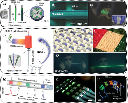
Flexible wearable devices based on ZnS. (a) Methods to enhance the binding of ZnS/PDMS with the fiber frame: increasing adhesion force and employment of an adhesive layer. The schematic on the right shows a cross-section of an ML fiber. (b) An enlarged image of a weft thread under UV light (365 nm) irradiation. (c) ML luminescent fabric after manual stretching. Reproduced with permission from Ref. [280] Copyright 2017, WILEY-VCH Verlag GmbH & Co. KGaA, Weinheim. (d) Improved melt-spinning for ML fibers, with the screw extruder changing from blue to red indicating the transition from the low-temperature zone to the high-temperature zone. (e) Fabric woven using SOEFSs and spandex as weft threads and cotton as warp threads. (f) Photograph of an electronic textile based on SOEFSs. Scale bar: 5 cm. (g) Light signals generated by stretching SOEFSs for underwater information interaction. Reproduced with permission from Ref. [281]. Copyright 2021, Wiley-VCH GmbH. (h) Schematic of mp-DOF comprising elastic waveguides and embedded ML pads (ZnS:Cu2+/Mn2+, ZnS:Cu2+, and ZnS:Cu+). (i) Optical image of a single-layer 4 × 4 array of mp-DOFs under 40 N pressure. (j) An integrated device photograph, including an elastic brace, a double-layer array with multi-colored contact points, and a flexible circuit module. Reproduced with permission from Ref. [21]. Copyright 2022, The Author(s), under exclusive license to Springer Nature Limited. ML, mechanoluminescence; mp-DOF, mechanoluminescence-powered distributed optical-fiber; PDMS, polydimethylsiloxane; SOEFSs, self-powered optoelectronic synergistic fiber sensors; ZnS, zinc sulfide.
Yang et al. used a novel thermoplastic polystyrene material instead of PDMS to prepare ML fibers.281 This material could be dissolved in a mixed solvent of cyclohexane and paraffin oil, allowing for the recycling of ML phosphors and repeated textile production, meeting both durability and environmental requirements. Figure 34d shows the process of ML fiber fabrication, where hollow core yarns are introduced into the extrusion head, and the core and ML composite material are extruded and thermally stretched on a hollow spinning plate. By adjusting the stress of the ML composite material, a helical structure can be introduced into the straight core yarn owing to friction between the sheath and core materials. This structural design allows DML and TML to occur simultaneously during yarn stretching–retraction, synchronously producing light and electrical signals. Consequently, the overall ML intensity improved by approximately 30% compared to DML alone, and by optimizing the spatial and surface charge polarization coupling effects through altering the ML powder ratios, the overall triboelectric performance increased by 100%. Figure 34e,f shows woven luminescent fabrics with alternating ML fibers and spandex as warp threads and cotton yarn as weft threads, offering high tensile properties and comfort in the warp direction. Figure 34g shows the excellent water-resistant and luminescent properties of the ML fiber.281
Biting can be used to generate signals in special situations, providing precise control and a new form of interaction for individuals with limited mobility. Hou et al. designed an interactive orthodontic device embedded with ZnS:Cu2+/Mn2+ (595 nm), Cu2+ (525 nm), and Cu+ (475 nm) ML phosphors within optical fibers, strategically positioned at predetermined locations (Figure 34h).21 These phosphors could modulate orange, green, and blue ML when distributed pressure was applied externally to the optical fibers. By detecting the fluorescence luminance ratio of unique bite points on the orthodontic device, various mechanical deformations on the lateral position could be distinguished. When combined with machine learning algorithms, this device could convert complex bite patterns into precise data input, enabling the interactive orthodontic device to operate computers, smartphones, and wheelchairs.
Figure 34i shows the pressure distribution and light propagation characteristics using a 4 × 4 single-layer array under different force modes. Figure 34j shows a three-dimensional (3D) printed soft orthodontic device incorporating a 2 × 3 single-layer sensor array with six pressure points. Two highly sensitive color sensor chips are positioned at the sensor's end and linked to a flexible processing circuit, allowing effective bending to accommodate the orthodontic device's interior, achieving high-precision sensing. Similarly, Liang et al. and Zhou et al. integrated ML materials with PDMS coated on the surface of optical fibers to create high-precision strain sensors282 and distributed optical fiber strain sensors,121 demonstrating stress durability exceeding 10,000 and 8000 cycles, respectively.
The EL characteristics of ZnS are also frequently used in the fabrication of smart textiles with large-area display capabilities.283 When activated by AC electric fields on a polymer matrix, these textiles can serve as real-time communication tools for individuals with speech or language difficulties. The improved EL fibers are compatible with existing textile processes,64, 283 demonstrating good abrasion resistance and resistance to washing. Shi et al. presented a comprehensive textile system, including a display screen, keyboard, and power source (Figure 35a,b).64 They used an industrial loom to weave conductive warp yarns and luminescent weft yarns together with cotton yarn. Each interwoven warp and weft yarn formed an EL unit, and when they came into contact, the circuit was completed, resulting in light emission. These textiles featured evenly spaced EL units, with less than an 8% relative deviation in brightness among 600 EL units. Even after repeated folding in different directions, most EL units exhibited intensity variations of <15%, and EL units along the fold line maintained stability after 10,000 folds, which indicated higher durability compared to traditional thin-film displays, with average brightness comparable to commercial flat-panel displays. As these fibers were woven, the density of EL units could be readily modified by adjusting the weaving parameters, which alters the spacing between the warp and weft intersections. They could also be sewn using nylon and cotton threads to accommodate various applications. Moreover, apart from creating EL fibers and then weaving or incorporating them into existing textiles, more lightweight and highly extensible smart textiles could be obtained by altering the physical structure of the textile. For example, Wu et al. demonstrated an open framework structure for ultra-thin textiles based on ZnS:Cu, reaching the strain limit of the textiles (200%). They designed electrode patterns on the textile and combined them with a soft contact layer to create luminescent textiles (Figure 35c–e).284
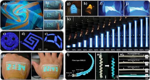
(a) Functional multi-color display textile under deformations. Scale bar: 2 cm. (b) Inputting information onto the clothing via buttons on the textile. Scale bar: 2 cm. Reproduced with permission from Ref. [64]. Copyright 2021, The Author(s), under exclusive license to Springer Nature Limited part of Springer Nature. (c–e) Photographs of light-emitting textiles displaying (c) the “smiling face” emoji, (d) a rectangular spiral, and (e) the number 8. Reproduced with permission from Ref. [284]. Copyright 2020, Elsevier Inc. (f) Luminescent images of the display attached to the back of the hand, serving as an epidermal stopwatch. Reproduced with permission from Ref. [279]. Copyright 2019, American Chemical Society. (g, h) Images of the device under different deformations (wrapped around a finger). Device thickness is 5 mm, with each pixel size being 4 mm (among 64 pixels). Reproduced with permission from Ref. [261]. Copyright 2016, The American Association for the Advancement of Science. (i–k) Luminescent operation photographs of ACEL devices under twisting (i), further stretching (j), and stretching (k) up to 1400%. Reproduced with permission from Ref. [285]. Copyright 2023, Wiley-VCH GmbH. (l) The structure of the fiber-type SSELD, including core (stainless steel wire), luminescent shell (viscoelastic light-emitting composite, VLC), and outer shell (ionic liquid). (m) Photographs of the SSELD in AC electric-field-off (left) and electric-field-on (right) states. The voltage amplitude is 175 V, and the frequency is 1 kHz. (n) Self-healing and luminescence process of the SSELD. (i) after the mechanical damage; (ii, iii) after 10 and 30 min self-healing. (iv) Under the same voltage as in (m), after 30 min of the healing process. Reproduced with permission from Ref. [286]. Copyright 2018, Wiley-VCH Verlag GmbH & Co. KGaA, Weinheim. ACEL, alternating current electroluminescent; SSELD, shape-deformable and self-healing EL display.
Owing to the excellent mechanical properties of ZnS itself, ZnS-based ACEL devices typically exhibit strong deformation resistance, as long as the composite materials are appropriately chosen. For example, PVDF is a polymer with a high dielectric constant that can effectively concentrate the electric-field-on fluorescent powder particles, thereby increasing the charge on the fluorescent powder particles and enhancing the light intensity.279 Zhou et al. introduced ZnS into a PVDF-HFP elastomer to create stretchable dielectric nanocomposites and prepared them as stretchable ACEL devices.279 These devices could operate at low voltages ranging from 10 to 35 V. They were mounted on the back of the hand using a silicon-based adhesive, ensuring conformal and intimate interaction with the skin. When this device displayed numbers (such as a stopwatch), it exhibited excellent deformation resistance, allowing it to continue functioning as the wearer made various hand gestures (Figure 35f). Go et al.285 combined Ecoflex with ZnS to create electronic skin and ACEL devices. These devices could still emit light when driven by AC even under various deformations such as bending and twisting (Figure 35g–j).
As shown in Figure 35k, during the initial stages of stretching, as the strain increases, the brightness increases to 395 cd · m−2 owing to reduced emission layer thickness and subsequent electric field enhancement. For stretches exceeding 800%, the brightness decreases with rapidly increasing stretch, attributable to the increased electrode resistance. However, at 1400% stretch, the measured brightness remains at 234 cd · m−2, comparable to the initial state. Importantly, the emitted light maintains its color throughout the stretching process.285 Moreover, if the ACEL devices are combined with self-healing polymer materials such as polyacrylic acid and PU, shape-deformable and self-healing EL display can be achieved (Figure 35l–n).149, 287, 288 Finally, as was the case for the ACEL devices' electrode materials, the materials here included Ag nanowires,283, 289, 290 carbon nanotubes,275, 291, 292 conductive polymers,149, 293 graphene,294 and their hybrids.295, 296 Moreover, the electrode shape could be designed in a wave-like form to enhance their overall stretchability and durability.290
TENGs are also an important means of obtaining AC electric fields, enabling self-powering capabilities for devices.297 Zhao et al. created an electronic skin comprising a ZnS:Cu/Al3+ ML layer, aluminum electrodes, insulating layer (Kapton), shielding layer (aluminum), and PDMS substrate.298 This electronic skin could sense pressures as low as 20 kPa and, when integrated with a microcontroller, could be used as a programmable touch interface supporting over 156 interactions. In some studies, the ML effect has been used to enhance the sensitivity of electronic skin. Jang et al. fabricated pressure-sensitive MoS2 field-effect transistors incorporating ZnS ML particles and an air dielectric layer as a tactile pressure sensor array. Pressure applied to the ZnS elastic material generated ML, considerably enhancing its sensitivity to pressure and producing additional photocurrents in the MoS2 channel, extending the detection range from 200 Pa to 5 MPa (for a wide range of pressure distribution).116
6.3 Battery-free display
ZnS light sources exhibit multimode conversion properties, allowing for visualization of not only mechanical forces but also responses to airflows,63, 195 magnetic fields,299 AC electric fields,150 and even moisture,300 boasting potential applications in different scenarios and extreme environments.279, 301 Their implementation is primarily achieved by fabricating devices through the composite of ML materials with substrates such as PDMS. Tuning the ML color can be accomplished by blending different ML materials or by combining them with fluorescent dyes.56, 263, 302
In outdoor environments, wind energy is one of the most common forms of mechanical energy that can be used to drive ML. Jeong et al. demonstrated an ML display driven by airflows, suitable for large-scale passive outdoor displays.63 The pixel units of this display comprised ML rods, which were formed by mixing ZnS with PDMS and curing them in molds. Under the impact of N2 airflow, the rods vibrated and generated ML along the direction of the airflow (Figure 36a). It is worth noting that rods close to the airgun did not vibrate and thus did not produce ML. As the distance increased, the irregularity of the wind direction increased owing to interactions between the rapidly diffusing gas and the aligned rods. Typically, ML emission was evident only twice—that is, during the gas injection and gas cessation. However, natural variations in the wind direction can be complex, so further improvements in the display structure are needed to adapt to different wind directions.63
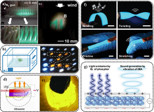
(a) ML under continuous N2 airflow: (i) ML panel; (ii and iii) magnified photographs of rods near to and far from the air duct; (iv) a pattern of ML. Reproduced with permission from Ref. [63]. Copyright 2014, The Royal Society of Chemistry. (b) Schematic of ML induced using an experimental ultrasonic cleaner. (c) ML image containing encrypted information (Z). Reproduced with permission from Ref. [254]. Copyright 2018, The Royal Society of Chemistry. (d) Schematic of the device used to measure the luminescence and ultrasonic characteristics of ZnS:Mn2+ films on a PMN-PT substrate under an AC electric field. (e) Luminescent photograph of the ZnS:Mn2+ film, taken while applying a voltage at a frequency of 500 Hz and an amplitude of 200 V. Reproduced with permission from Ref. [303]. Copyright 2012, Wiley-VCH Verlag GmbH & Co. KGaA, Weinheim. (f) Operation of the sound-in-display device with sound-synchronized EL under different mechanical deformations, under the application of a square pulse function (60 V, 5 kHz). Scale bars: 1.5 cm. (g) Schematic diagram of the device generating light emission and sound. Reproduced with permission from Ref. [113]. Copyright 2020, The Authors. Published by Wiley-VCH GmbH. EL, electroluminescent; ML, mechanoluminescence; PMN-PT, Pb(Mg1/3Nb2/3)O3-xPbTiO3.
In this research, the mechanical strength of the ML rods cured directly from ZnS/PDMS was limited. If the size of ML rods was reduced to improve the resolution, there was a risk of detachment. Consequently, it was determined that an appropriate microcolumn diameter should be 1 mm (approximately 12.7 ppi). This problem could be partially addressed by preparing the material in a thin-film structure, which can withstand greater friction and is easier to integrate with other devices.303 Furthermore, aside from direct display applications, ML can also be used to charge solar cells at night through the photoelectric effect,304 thereby enhancing the energy storage efficiency of solar cells.305
ZnS-based devices can achieve mutual conversion among ultrasound, optical energy, and electrical energy through clever structural design. Li et al. reported highly porous composite materials, prepared from PVDF-HFP and ZnS, capable of converting ultrasound into optical signals.254 Their efficient ML performance resulted not only from the porous structure of the films but also from the strong interaction between the PVDF-HFP and ZnS. The porous structure facilitated the conversion of mechanical forces into electrical energy and induced ML in the ZnS. Moreover, the particle–film interaction induced a high proportion of the β-phase (a notably effective piezoelectric phase) in the PVDF-HFP film. Consequently, this composite film could be excited to produce ML in a laboratory ultrasonic cleaning tank (Figure 36b). Figure 36c shows an array based on this composite material, forming the letter Z under ultrasound vibration.254
Zhang et al. grew ZnS:Mn2+ thin films on a piezoelectric Pb(Mg1/3Nb2/3)O3-xPbTiO3 (PMN-PT) substrate, enabling the simultaneous conversion of electrical signals into optical signals and ultrasound (Figure 36d,e). This was achieved through the inverse piezoelectric effect in PMN-PT.303 This novel dual-mode light source for ML and ultrasound emission, integrated with a detection system on a single chip, holds considerable promise for the development of hybrid systems for tissue diagnostics.108, 306, 307
Similarly, dielectric elastomer actuators (DEAs) can generate mechanical motion when subjected to an electric field, displaying outstanding mechanical actuation performance with area strains exceeding 200%.308, 309 Wang et al. integrated DEAs with stretchable EL devices, demonstrating a self-shaping ACEL device.150 Compared to traditional ACEL devices, this special device exhibited dynamic shape display capabilities and could achieve approximately 55% area strain under an excitation voltage of 5 kV. Cho et al. created a stretchable sound display device capable of producing synchronized audio and visual information (Figure 36f).113 The device incorporated a stretchable EL loudspeaker based on ZnS:Cu emitting layers and a matrix of DEAs positioned between stretchable electrodes (Figure 36g). When an AC bias voltage was applied to this speaker, the emitting layer underwent EL, generating audible sound waves through the vibration of the DEA matrix. Consequently, the intensity of both light emission and sound could be adjusted by varying the bias voltage parameters.
The detection of magnetic fields is crucial for environmental monitoring, mineral exploration, and safety surveillance applications, and ML materials can be applied in this context.310 Compared to traditional magnetic sensors, they offer advantages of non-contact, non-destructive, and non-invasive detection.61, 311 Wong et al. embedded soft magnetic particles into PDMS to create a composite layer, which could produce magnetostrictive strain in a magnetic field, triggering adjacent ZnS/PDMS layers to emit ML, as shown in Figure 37a. When the magnetic field frequency was modulated from 50 to 470 Hz, the emission color shifted from green to blue, and the intensity changed too (Figure 37b).310 Listyawan et al. developed a magnetic field-driven lighting device without electricity sources. This device comprised a Kirigami-shaped ZnS/PDMS composite and a magneto-mechano-vibration cantilever beam, capable of generating ML under magnetic field drive (Figure 37c). This structure reduced rigidity and increased stretchability, promoting ML generation (Figure 37d).299
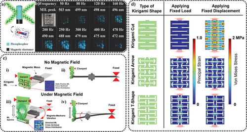
(a) Schematic of a magnetic field exciting ZnS ML composite material. (b) Relationship between the magnetic field modulation frequency and ML intensity and color. The color shifts from green to blue as the frequency increases. Reproduced with permission from Ref. [310]. Copyright 2017 Wiley-VCH Verlag GmbH & Co. KGaA, Weinheim. (c) Schematic diagram of the magnetically driven powerless lighting device, comprising Kirigami-structured ZnS:Cu/PDMS and an MMV cantilever. (i, ii) Static mode of the device (without magnetic field) and its side view (showing no deflection). (iii, iv) The device in dynamic mode (with magnetic field) and its side view demonstrates the cantilever structure vibrating owing to magnetic torque, which results in luminescence from the edges of the Kirigami-structured ML section. (d) FEA results of different Kirigami structures under specific boundary conditions: a fixed load (total force: 0.7 N) and a fixed displacement perpendicular to the cuts (150 mm), where the red arrows show the direction of displacement and the applied load. Reproduced with permission from Ref. [299]. Copyright 2023, The Authors. Advanced Science published by Wiley-VCH GmbH. FEA, finite element analysis; ML, mechanoluminescence; MMV, magneto-mechano-vibration; PDMS, polydimethylsiloxane; ZnS, zinc sulfide.
The aforementioned magnetic-mechanical-optical energy transformation exhibited low conversion efficiency and produced weak light emission. In another approach, Yang et al. leveraged the EL properties of ZnS:Cu to achieve battery-free, high-brightness light emission, applying electromagnetic-electric-optical energy transformation, which could be more suitable for harnessing electromagnetic energy.148, 312 They developed a sophisticatedly structured interactive fiber to realize this function. First, this kind of fiber could serve as an antenna, and the electromagnetic field in the environment (simulated by applying a 30-dBm/∼20-kHz transmitter) could induce an electromotive force within the fiber, charging a capacitor. Subsequently, when the human body contacted the fiber, a closed-loop circuit was formed between the fiber, the human body, and the earth. The electrical energy stored in the capacitor was then rapidly discharged (Figure 38a). Owing to the high dielectric constant of the human body, when the finger was in close proximity to the interactive fiber, the momentary high voltage caused air breakdown, resulting in local plasma discharge (Figure 38b,c), leading to the simultaneous emission of electromagnetic waves and light, with the light emission facilitated through the EL properties of ZnS:Cu. Under 21.1°C and 46.8% relative humidity conditions in office, the brightness could reach up to 270 ± 11 cd · m−2. This kind of intensity makes it possible to use the technology in various battery-free display scenarios, such as interpersonal information exchange and friction-driven luminous carpets (Figure 38d–h), holding great promise for the integration of ML properties to enhance the overall luminosity and energy conversion efficiency.
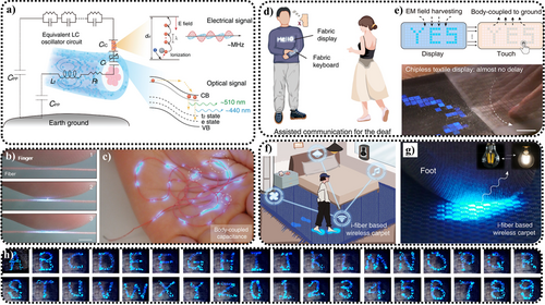
(a) Structure of the interactive fiber and its principle for the simultaneous emission of light and electromagnetic waves. This fiber comprises three parts: the core conductor (silver-plated nylon fibers, pink), the dielectric layer (BaTiO3 mixed resin, white), and the luminescent layer (ZnS:Cu mixed resin, blue). The internal conductor can be considered to be a combination of inductors and resistors; the longer its length, the stronger the induced electromotive force. When a finger approaches the fiber, the air becomes ionized, leading ions and electrons to clash and migrate in turn at high speed among air molecules in the gap. This results in an additional rapidly changing electric displacement field, generating the emission of electromagnetic waves; simultaneously, the instantaneous discharge also induces EL in ZnS:Cu. (b), (c) Effects of air ionization and light emission when a finger contacts the fiber, at the contact point. Scale bar: 3.5 mm. (d–g) Schematic illustrations of information interaction and display based on the interactive fabric that emits light under the friction of fingers or soles. Scale bar: 3 cm. (h) Display effects of 36 letters and 10 numbers achieved with the interactive fabric. Reproduced with permission from Ref. [148]. Copyright 2024, The American Association for the Advancement of Science. EL, electroluminescent; ZnS, zinc sulfide.
Finally, as is evident from the applications discussed in the previous three chapters, printing technology has been used extensively, making it one of the most common methods for fabricating ML materials into fibers, arrays, patterns, and other application forms.34, 305, 313-315 For ZnS, 2D printing is often done using screen printing to form thin-film structures on paper or ceramic pieces.111, 162 3D printing techniques commonly used for ZnS include direct-write printing and extrusion-based 3D printing. For example, Qian et al. prepared printable inks based on ZnS/SiO2/PDMS, where SiO2 nanoparticles added to the ink fully infiltrated and adhered tightly to the PDMS polymer chains (forming Si-O bonds),66 allowing for better transmission of pressure to the ML crystals. Zhao et al. used extrusion-based 3D printing and ZnS:Cu/SiO2/PDMS ML ink to create periodic honeycomb structures.316 When subjected to uniaxial stretching, these two structures alternately produced anisotropic and isotropic light emission.
Moreover, Li et al. developed a universal strategy for laser direct printing of inorganic nanomaterials, which eliminated dependence on photocurable resins during the printing process, enhanced the content of ML materials, and improved the overall ML performance of composites.317 Moreover, this method exhibited extremely high compatibility with materials and offered considerable printing freedom. In their research, they printed over 10 types of semiconductors, metal oxides, metals, and their mixtures, including CdSe/ZnS core-shell QDs. Colloidal nanocrystals served as building blocks and could be chemically bonded through their native ligands. Without the need for resins, this bonding process could produce arbitrary 3D structures with over 90% inorganic mass fraction and high mechanical strength. This technique opens up new possibilities for designing and fabricating advanced materials and devices with tailored properties and structural complexity.
6.4 Biomedical imaging
In the field of biomedical research, ZnS has been applied primarily in the areas of bio-inspired skin, vivo imaging, and therapy.318-320 As biological tissues and organs are opaque, it can be practically impossible to directly observe the physiological conditions of internal organs with the naked eye. Consequently, biomedical sensors are essential for real-time imaging and observation of internal organs. ML sensors have the advantage of being able to directly convert mechanical forces within the biological body into light emission. Compared to traditional biomedical sensors, they offer simplicity in structure, high complexity, good self-recovery properties, and excellent biocompatibility.
Kim et al. developed an artificial cochlea (Figure 39a,b) using a ZnS:Cu/PDMS composite film as the human basilar membrane (BM), which could simulate the phenomenon of upward wave propagation on the BM in the human cochlea.321 When the ML BM was subjected to acoustic waves, it produced its maximum wave amplitude at different positions, inversely proportional to the frequency of the sound waves. By measuring the position of ML emission on the BM using a non-contact image sensor, the frequency information of the sound waves could be obtained. This method had a theoretical resolution that was infinite (continuous), as it was not limited by traditional artificial cochlea BM arms or hair cell numbers, and could achieve real-time imaging and wireless sensing of mechanical stress within the biological body. As shown in Figure 39c, with increasing excitation frequency, the peak position moves from the apex to the base of the ML BM. The wave travels from the base to the top, and the position of the maximum wave amplitude shifts considerably from the top to the base as the stimulus frequency increases. At high frequencies (150 Hz), the shape of the envelope of the wave tilted slightly near the base, whereas at low frequencies (25 Hz), it tilted slightly near the apex. However, the shape of the wave envelope did not change significantly at low frequencies. This observation confirmed the velocity input response of the ML BM to the oval window at different frequencies. Simulation observations from the Finite element analysis (FEA) clearly showed that the prototype artificial cochlea using the ML BM exhibited similar frequency selectivity compared to the human cochlea.321
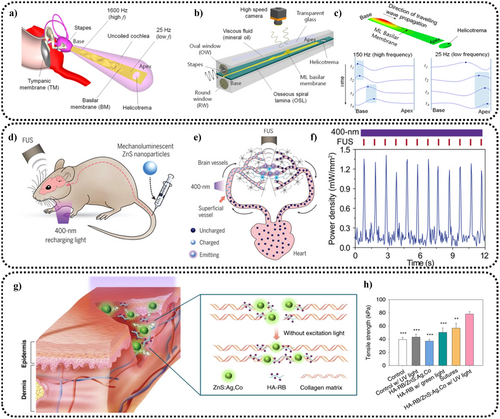
(a) Frequency selectivity of different regions of the basilar membrane. (b) Illustrative diagram of the artificial cochlear structure on the ML basilar membrane, where the traveling wave enters the cavity infiltrated with viscous fluid (mineral oil) through the oval window, causing the human basilar membrane within to emit optical signals, which are collected using a high-speed camera. (c) Propagation modes at different frequencies demonstrating frequency selectivity. Reproduced with permission from Ref. [321]. Copyright 2018, The Author(s). (d) Schematic of the experimental procedure. ZnS nanoparticles are injected intravenously into the mouse tail, a 400-nm light source is positioned near the neck skin, and a focused ultrasound transducer is placed above the mouse's head. (e) Schematic of blood circulation of nanoparticles. 400-nm light is used to excite the surface vessels, charging the nanoparticles. Subsequently, these particles are transported through the bloodstream to deep brain regions, where they are excited by ultrasound to emit 470 nm light, stimulating the mouse brain. (f) Circulation, excitation, and charging of ZnS:Ag+/Co2+@ZnS nanoparticles, measuring the equivalent power density of 470 nm light emission in brain tissue using repeated focused ultrasound stimulation (red scale) and continuous 400-nm charging light (purple bars). Reproduced with permission from Ref. [67]. Copyright 2019, the Author(s). Published by PNAS. (g) Photocoupling of the HA-RB/ZnS:Ag+/Co2+ mixture on a sliced collagen matrix under UV light exposure. (h) In-vivo tensile strength of different groups of skin wounds on the third day (4 samples/each group, “w/” is “with”; “*” denotes “p < 0.05”; “**” denotes “p < 0.01”; “***” denotes “p < 0.001”). Reproduced with permission from Ref. [322]. Copyright 2022, The Author(s). ML, mechanoluminescence; ZnS, zinc sulfide.
In terms of in vivo light sources, Hong et al. used extracorporeal ultrasound-focused excitation to trigger luminescence from ZnS:Ag+/Co2+@ZnS ML particles in the blood, enabling non-invasive detection from inside to outside (Figure 39d,e).67, 93 Initially, the ZnS:Ag+/Co2+@ZnS core-shell nanoparticles were intravenously injected into mice as light sources. As they flowed with the bloodstream into brain vessels, the continuous blood flow ensured a constant supply of luminescent light sources to the brain vasculature. Through excitation using FUS applied externally to the mice, via the intact skull and skin, the ZnS:Ag+/Co2+@ZnS nanoparticles in the mouse's blood emitted blue visible light, which could be charged using 400-nm UV light through surface-level veins. Subsequently, under the FUS excitation, 470-nm light emission could be generated, enabling non-invasive diagnosis of the optogenetic status of the mouse's brain (Figure 39e). Imaging sensors were used externally to visualize the luminescence within the body, equivalent to an effective power density of approximately 1.2 mW · mm−2 (Figure 39f).93 Moreover, the composite of ZnS ML nanomaterials with graphene could be used to create pulse sensors capable of sensing forces from 0 to 20 N.207
Photodynamic tissue bonding (PTB) is a new technology for trauma closure. This method employs light and photosensitizers to enhance collagen cross-linking, minimize inflammation, and lessen scarring. One frequently used photosensitizer in PTB is Rose Bengal dye. This dye captures energy from green light and reacts with collagen, producing radicals that facilitate the formation of covalent bonds among collagen molecules. Kim et al. used the long AL of ZnS:Ag+/Co2+ to stimulate the collagen matrix inside cut tissue for PTB (Figure 39g).322 In the depth direction of skin closure incisions, the emission intensity of ZnS:Ag+/Co2+ particles at 540 nm remained robust, while the intensity of the green laser at the same wavelength decreases exponentially with skin depth. Within 30 s, the AL intensity of ZnS:Ag+/Co2+ particles significantly exceeded that of the green laser. This indicates that the green light from ZnS:Ag+/Co2+ particles can be efficiently transmitted to deeper tissue layers for sustained tissue bonding. Figure 39h shows the consistent increase in collagen fiber formation over a stable time point of 6 min. The results confirmed that using intermittent UV irradiation with a hyaluronate-RB/ZnS:Ag+/Co2+ mixture could accelerate collagen cross-linking more effectively than traditional PTB using green light.322
6.5 Deep learning and optical information processing
To date, machine learning and deep learning methods have been used primarily to extract information from ML signals or as auxiliary tools to enhance the accuracy of the information retrieval process. In this chapter, various models are introduced for processing ML information related to handwritten digits, crack propagation, and limb movement. It should be noted that the models currently applied to ML data processing are relatively simple, partly owing to the ongoing research in this field and partly limited by the accuracy of the CMOS and ML sensors themselves.
Zhou et al. used the random forest machine learning algorithm to recognize handwritten digits generated by ZnS:Cu sensors (Figure 40a–c).323 In their experiments, the network was pre-trained using the MNIST handwritten database, and handwritten-digit images were generated by extracting and overlaying consecutive frames from videos of handwritten digits. The green component was isolated to eliminate the influence of red and blue light, and after binarization, it was input into the network for digit recognition. The experiment compared the accuracy of three machine learning methods—that is, the random forest, K-nearest neighbors, and decision tree models—with the random forest model achieving the highest accuracy. After training with 60,000 handwritten digits, it achieved approximately 96.87% recognition accuracy on another dataset of 10,000 handwritten digits.
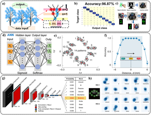
(a) Schematic diagram of the random forest machine-learning algorithm. (b) Prediction confusion matrix based on 10,000 test data. (c) Demonstration of the handwritten digit-controlled small car motion system. Reproduced with permission from Ref. [323]. Copyright 2023, The Author(s). (d) The ANN model used in the experiment. (e) Classification results of 14 bite patterns using ANN for ML data classification, where ∆x = x1 − x2 and ∆y = y1 − y2. Each pattern's data is marked with the same symbol, the red dots representing the average chromatic response of each pattern. (f) Relationship between the recognition accuracy and bite position offset (distance) within an 8-mm distance (blue shaded area), where recognition accuracy is >75%. The inset illustrates the bite motion path. Reproduced with permission from Ref. [21]. Copyright 2022, The Author(s), under exclusive license to Springer Nature Limited. (g) The network architecture of VGGNET-5 includes five feature extraction layers. (h) Motion patterns of two patches near the mouth (ROI-1 and ROI-2) under different meanings. Reproduced with permission from Ref. [324]. Copyright 2022, Wiley-VCH. ANN, artificial neural network; ML, mechanoluminescence.
Compared to traditional methods, such as digital image correlation or FEA methods combined with ML for crack inspection—machine learning, and deep learning algorithms can achieve higher accuracy and real-time quantitative analysis. Zhang et al. proposed a machine-learning-based fatigue crack propagation detection method, where seven different models were used to classify cracks. The decision tree model exhibited the highest accuracy, with a crack length measurement precision of 0.6 mm.325
Ahn et al. employed the generative adversarial network (GAN) and convolutional neural network (CNN) to process ML and FEA images. The GAN was trained to convert real ML images into virtual FEA images (or vice versa), whereas the CNN was trained to derive a Kp value from the FEA or ML data as an alternative to traditional numerical solutions. This dual AI approach provided more accurate results compared to pure ML solutions. Moreover, it could also provide far-field stress distribution, achieving similar accuracy to real computed FEA while substantially reducing time and costs.326
In the design of a wearable bite device by Hou et al., two ML optical fibers were used, each containing three ML blocks that emitted green, yellow, and orange light.21 The spectral information of these three lights was combined into three stimulation values using a color sensor, resulting in six data points (X1, Y1, Z1; X2, Y2, Z2). These data were transmitted via Bluetooth to a computer for analysis (after conversion to CIE XYZ color space data [x1, x2; y1, y2]) (Figure 40d–f). There were a total of 21 bite modes, of which 14 were used for testing and training, with over 300 data points obtained for each mode. If a simple scheme of threshold classification based on CIE values was adopted, the overall recognition accuracy was only 89%. Not only was it difficult to set the threshold, but the set threshold also struggled to meet the goal of precise classification. Consequently, they employed a two-layer feedforward ANN for data analysis, with the ANN comprising 4 input nodes, 14 output nodes using a SoftMax function, and 10 hidden nodes with a sigmoid activation function. After training, this approach increased the accuracy to 98%.21
Deep learning is not only used for processing ML data but can also handle AL variation data, which is important for materials like SrAl2O4. Timilsina et al. used two CNN-based neural networks—that is, the Visual Geometric Group network and residual neural network (ResNet-34), to learn from fluorescent images.324 They achieved recognition accuracies of 98.5% and 98.75% for 10 pieces of information, including seven words, two letters, and a smiling mouth (Figure 40g,h). This work involved attaching eight long AL patches around a person's mouth emoji. When the person expressed different meanings, such as “around” or “ground,” the motion patterns of the eight fluorescent patches varied. Ten frames were selected and overlaid for each scenario, converted to grayscale, and then input into the neural network to extract information. To avoid overfitting, each stacked image was augmented with five copies generated by random transformations including rotations, scaling, flipping, and translations during training.
Combining target recognition neural networks with the variation of ML images may be used for a new generation of motion force sensors and systems (Figure 41a). ML images from objects have the feature that their luminescence intensity is proportional to the magnitude of the motion force, and they exhibit sustainable repeatability and self-recovery (Figure 41b,c). With the development of deep learning networks, precise capture and recognition of motion image information has already been achieved (Figure 41d).328, 329 Therefore, soft sensors based on ML materials can be worn on different parts of the body. When a part of the body moves and emits light, the neural network can recognize the location and amplitude of the motion force, achieving precise motion force sensing (Figure 41e,f). Chun et al. have proposed an interactive wearable display by integrating multicolor perovskite and ZnS materials, powered by an external energy source (Figure 41g,h).276 If self-powered ML materials are used instead of external energy, it is expected to create an interactive motion sensing system that meets the requirements of low energy consumption and high precision. Hou et al.'s research has preliminarily verified the feasibility of this concept.21 They achieved motion force pattern analysis of tooth occlusion in a small area of the oral cavity to output control signals (Figure 41i). Looking ahead, expanding this approach to large-scale motion force monitoring could result in a more comprehensive and interactive intelligent sensing system.
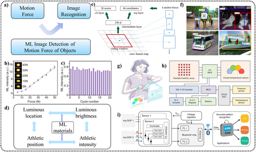
(a) Utilizing ML materials to convert the kinetic force of moving objects into visual images, thereby achieving intelligent recognition of kinetic forces through image recognition. (b–d) The luminescence intensity of ML materials is proportional to the magnitude of the kinetic force (b), and their high reproducibility (c) makes them suitable for visualizing and imaging unknown kinetic force intensities (d). Reproduced with permission from Ref. [327]. Copyright 2020, Science China Press. (e, f) Object imaging detection is driven by the region proposal methods and region-based convolutional neural networks, which detects objects in a wide range of scales and aspect ratios. Reproduced with permission from Ref. [328]. Copyright 2017, IEEE. (g) Conceptual image of the smart human-device interaction display. (h) The system configuration of the skin-conformable perovskite-based ACEL devices. ADC, analog-to-digital converter; HV MUX, high-voltage multiplexer; MCU, microcontroller unit. Reproduced with permission from Ref. [276]. Copyright 2024, The Author(s). (i) Interactive force sensor control flow chart. ADC, analog-to-digital converter; VDD, the operating voltage of the digital circuit. Reproduced with permission from Ref. [21]. Copyright 2022, The Author(s), under exclusive license to Springer Nature Limited. ML, mechanoluminescence.
7 CONCLUSIONS AND OUTLOOK
7.1 Conclusions
This paper provides a comprehensive review of the history, materials, performance, synthesis, and application of ZnS ML, highlighting its considerable advantages in passive visual sensing, self-powered displays, and innovative light sources. ZnS demonstrates enormous potential in various fields, including flexible optoelectronics, materials science, engineering, and energy, owing to its luminescence mechanism that differs from traditional methods such as EL and PL. As a classic ML system, ZnS serves as an inspiration for the development of new intelligent ML systems, LED-like heterojunction high-brightness ML, and bio-inspired mechanical excitation luminescence models.
7.2 Future prospects
-
Optimization of ML properties of doped ZnS materials offers a major opportunity for innovation. Currently available ZnS materials are used primarily for commercial ACEL, which differs in its excitation method from ML. Therefore, there is considerable room for optimizing ML characteristics, including the impact of the material polarity and orientation, precise control of the crystal growth, preparation of zero-dimensional and two-dimensional thin films, and efficient nanostructures (such as QDs and superlattice single-crystal thin films). Although there have been detailed experimental studies on Mn-doped ZnS ML materials, research on Cu-doped ZnS ML materials remains relatively limited. The repeatability of fabrication techniques for high-brightness Cu-doped ZnS ML material requires further verification and optimization.
-
Clarifying the luminescence mechanisms of ZnS ML is crucial, as it is essential to determine whether ZnS ML originates from deformation-induced luminescence or frictional-EL mechanisms. This includes rigorously verifying the ACEL mechanism and eliminating the possibility of deformation-induced luminescence caused by frictional deformation if the frictional-EL hypothesis is proposed. Moreover, the investigation of ML variations at high frequencies has emerged as a recent research focus, making it imperative to explore how different doping agents, particle sizes, and alterations in internal energy transfer processes can affect ML characteristics.
-
Advancing the fabrication of high-performance devices requires a focus on several innovative technologies. Key areas include the development of large-area wearable fibers, the integration of machine-learning enhanced sensor systems, advances in 3D printing, and the use of optical fiber technology. Further exploration is needed in advanced low-light detection and single-photon detection systems, alongside new structural designs such as LED-like heterojunction structures. Effective control of defects and the strategic design of electron–hole pair defects are also critical. Moreover, research should expand into monitoring applications using multimodal excitation, including traditional optical excitation methods such as UV-visible light, mechanical force excitation from environmental mechanical energy or ultrasound, molecular thermal motion energy, and interactions with X-ray and high-energy radiation/particle excitations. An important area of exploration involves research into whether luminescence characteristics induced by high-energy particle impacts can be applied to the detection of elusive particles such as neutrinos and dark matter.
-
Research into composite elastomer encapsulation techniques should prioritize the development and refinement of these methods, ensuring that they are effectively tailored for various applications. Conducting thorough compatibility testing with biological and environmental factors is imperative to guarantee their safety and functionality. Additionally, a detailed assessment of biotoxicity is crucial to confirm that these materials can be used safely in proximity to living organisms. Evaluating their weather resistance is vital to ascertain their ability to withstand different climatic conditions, thus ensuring their durability and reliability. Finally, rigorous service life testing must be conducted to determine the longevity and performance consistency of these encapsulated systems over time.
-
Identifying the foundational elements for high-performing self-recovering ML materials is crucial too. This involves establishing constitutive models that effectively map the relationships between the stress, structural characteristics, and luminescence properties. Such models can facilitate detailed comparisons of luminescence attributes across different ML materials, enhancing our understanding and development of new compounds. Moreover, the creation of a comprehensive material database is recommended, which could support the use of high-throughput algorithms and first-principle calculations to standardize material properties and behaviors, ensuring a robust framework for innovation. Additionally, developing standardized testing protocols and engineering test reports is essential, providing reliable guidelines for assessing the performance of new high-brightness ML materials and aiding in the design and optimization of future applications. Collectively, these initiatives could propel the advancement of the field, promoting the development of ML materials with superior recovery and luminescence capabilities.
AUTHOR CONTRIBUTIONS
Zefeng Huang: Conceptualization (lead); data curation (lead); formal analysis (lead); investigation (lead); methodology (lead); project administration (lead); validation (equal); visualization (lead); writing – original draft (lead); writing – review & editing (lead). Xu Li: Conceptualization (lead); data curation (lead); formal analysis (lead); investigation (lead); methodology (lead); validation (lead); visualization (lead); writing – original draft (lead); writing – review & editing (lead). Tianlong Liang: Conceptualization (equal); data curation (lead); investigation (lead); methodology (equal); validation (lead); writing – original draft (equal); writing – review & editing (lead). Biyun Ren: Conceptualization (equal); methodology (equal); writing – review & editing (equal). Xianhui Zhang: Writing – review & editing (equal). Yuantian Zheng: Writing – review & editing (equal). Qi'an Zhang: Writing – review & editing (equal). Ziyi Fang: Writing – review & editing (equal). Mingzhi Wu: Writing – review & editing (equal). Maryam Zulfiqar: Writing – review & editing (equal). Liqing Jing: Writing – review & editing (equal). Sicen Qu: Supervision (equal); writing – review & editing (equal). Bing Chen: Supervision (equal); Writing – review & editing (equal). Jiulin Gan: Supervision (equal); writing – review & editing (equal). Dengfeng Peng: Conceptualization (lead); data curation (lead); funding acquisition (lead); project administration (lead); resources (lead); supervision (lead); visualization (lead); writing – original draft (lead); writing – review & editing (lead).
ACKNOWLEDGMENTS
Z.H., X.L., and T.L. contributed equally to this work. The authors gratefully acknowledge the support of the Key-Area Research and Development Program of Guangdong Province (2024B0101080001), the Natural Science Foundation of China (grant nos. 62275170, 61875136 and 62205155), the Natural Science Research Start-up Foundation of Recruiting Talents of Nanjing University of Posts and Telecommunications (NY222104), the Guangdong Provincial Science Fund for Distinguished Young Scholars (2022B1515020054), Guangdong Province Philosophy and Social Science Planning Project (GD20XTY11), Foundation of Shenzhen Key Laboratory of Photonics and Biophotonics (ZDSYS20210623092006020), Scientific Research Foundation as Phase III construction of high-level University 2035 plan (0000050101) and the proof-of-concept project (000003011313) of Shenzhen University, as well as Medical-Engineering Interdisciplinary Research Foundation of ShenZhen University (2023YG031).
CONFLICT OF INTEREST STATEMENT
The authors declare that they have no known competing financial interests or personal relationships that could have appeared to influence the work reported in this paper.
Biographies

Zefeng Huang received his Master's degree (2023) from the College of Physics and Optoelectronic Engineering, Shenzhen University. His research is focused on smart luminescence direction, mainly researching and preparing mechanoluminescence material, strontium aluminate and related applications. He is now working as a research assistant at the Hong Kong University of Science and Technology (Guangzhou).

Xu Li received his Master's degree (2023) from the College of Physics and Optoelectronic Engineering at Shenzhen University. His research interests include the synthesis and application of mechanoluminescent materials. He is now pursuing his Ph.D. studies at The Hong Kong Polytechnic University (2024).

Tianlong Liang received his B.S. degree (2022) from the College of Applied Physics and Materials, Wuyi University. His research interests include the synthesis and research of new luminescent materials, such as mechanoluminescent and photoluminescent materials. He is now studying at Shenzhen University for his master degree, focusing on mechanoluminescence materials.

Biyun Ren received her Ph.D. degree (2021) in Materials Science and Engineering from City University of Hong Kong. Her research interests includes the synthesis and mechanistic investigation of lanthanide-doped nano/micro crystals. She is now carrying out postdoctoral research at Shenzhen University (2022), focusing on the fabrication and applications of mechanoluminescence nano/micro materials.

Xianhui Zhang is currently carrying out postdoctoral research at Shenzhen University (since 2022). He received his Ph.D. degree in Fujian Institute of Research on the Structure of Matter, Chinese Academy of Sciences & University of Chinese Academy of Sciences in 2022. His research interests focus on design and synthesis of the structural oriented optoelectronic functional materials, growth of large-size chalcogenide functional single crystals and mechanistic investigation of their photo-mechano-electrical under external fields.

Yuantian Zheng received his Master's degree (2023) from the College of Physics and Optoelectronic Engineering, Shenzhen University. His research interests include the synthesis and research of new luminescent materials, such as mechanoluminescent and photoluminescent materials. He is now studying at Xiameng University for his Ph.D degree, focusing on mechanoluminescence materials.

Qi'an Zhang received his B.S. degree (2023) from the College of Physics and Optoelectronic Engineering at Shenzhen University. His research interests focus on the synthesis and investigation of novel luminescent materials, such as mechanoluminescent materials. He is currently pursuing a Master's degree at Shenzhen University, specializing in mechanoluminescent materials.

Ziyi Fang received his B.S. degree (2023) from the College of Physics and Optoelectronic Engineering, Shenzhen University. His research interests focus on smart luminescence material direction. The primary research and preparation of simple oxides with self-recovering near-infrared mechanoluminescent properties and their related applications.

Mingzhi Wu received his B.S. degree (2023) from the College of Physics and Optoelectronic Engineering, Shenzhen University. His research interests include the synthesis and improvement of doped transition metal mechanolumine scentmaterials. He is now studying at Shenzhen University for his master degree, focusing on mechanoluminescence materials.

Maryam Zulfiqar received her Bachelor (2020) and Master Degree (2022) in Medical Physics from ISLAMIA UNIVERSITY, Pakistan. Now she is Pursuing a PhD Degree in College of Physics and Optoelectronics Engineering at SHENZHEN UNIVERSITY. Her research interests include synthesis, investigation and application of Mechanoluminescent Nanomaterial.

Liqing Jing received her Master's degree from Shenzhen University in 2012. Currently, she is employed as an experimentalist in the Key Laboratory of Optoelectronic Devices and Systems of the Ministry of Education and Guangdong Province, within the College of Physics and Optoelectronic Engineering at Shenzhen University. Her research mainly focuses on fiber optic sensing and non-imaging optical design.

Sicen Qu received her joint-M.S. degree in shenyang sport university, China and Gerlev Physical Education & Sports Academy in Denmark. He has been a lecturer in the College of Physical education at Shenzhen University since 2015. Her research interest is athletic analytics in sports sciences and Physical Education and Training.

Bing Chen received his B.E. (2012) and Ph.D. (2017) degrees in Materials Science and Engineering from Zhejiang University. He then carried out postdoctoral research work in Prof. Feng Wang's group at City University of Hong Kong. He joined Nanjing University of Posts and Telecommunications as a professor in 2022. His research interests focus on the development of luminescent micro/nanomaterials for sensing and imaging.

Jiulin Gan received his B.S. degree in optical information science and technology from Huazhong University of Science and Technology in 2006, and a Ph.D. degree in optical engineering from Shanghai Institute of Optics and Fine Mechanics, Chinese Academy of Sciences in 2011. Then, he went to South China University of Technology (SCUT, 2011) as a postdoctoral. Since 2013, he has been working as an associate professor and professor in SCUT. His research interests include fluorescence probe materials, composite optical fiber, fiber sensor and fiber laser, together with their applications in measurement and sensing.

Dengfeng Peng received Ph.D. degree (2013) in Materials Science and Engineering from Tongji University. He spent 1 year as a joint Ph.D. student at AIST in Japan (2012). He carried out postdoctoral research work at City University of Hong Kong (2013), Beijing Institute of Nanoenergy and Nanosystems, Chinese Academy of Sciences (2015), and The Hong Kong Polytechnic University (2016). He is now a professor in the College of Physics and Optoelectronic Engineering at Shenzhen University. His research interest includes the synthesis and mechanistic investigation of functional materials for applications in optoelectronic, flexible electronics and advanced energy devices.


