Polymorphic Phase-Change Properties and Memory Characteristics of VTe Thin Film
Abstract
Phase-change random access memory (PCRAM) is a leading candidate for emerging nonvolatile memory devices due to its fast switching speed, scalability, and complementary metal-oxide-semiconductor (CMOS) compatibility. However, traditional PCRAM relies on amorphous-to-crystalline switching, which suffers from high energy requirements and reliability issues. To address these challenges, in this study, the crystalline polymorphic phase-change behavior as an alternative, which eliminates reliance on the amorphous phase and its associated limitations, is investigated. Herein, the transition-metal tellurides, specifically a VTe binary system, are focused on and their potential for polymorphic phase transitions is investigated, leveraging insights from the crystalline polymorphic switching's dynamics of MnTe melting free phase-change material. The binary phase diagram of VTe suggests that the polymorphic transition between the V3Te4 and V5Te8 phases can be obtained in the composition of V:Te ≈ 0.4:0.6. In this study, a VTe thin film is deposited and its polymorphic transition properties are investigated. The associated electrical and optical property changes are also analyzed. Finally, a VTe-based memory device is fabricated and tested.
1 Introduction
The growing demand for efficient data storage and processing systems has driven the development of storage-class memory (SCM) technologies, thereby bridging the gap between conventional dynamic random-access memory (DRAM) and not AND (NAND) flash memory.[1-3] Among the various SCM candidates, phase-change random access memory (PCRAM) has emerged as a promising solution due to its unique combination of speed, scalability, and nonvolatility.[4-6] PCRAM employs phase-change materials, e.g., Ge2Sb2Te5 (GST), to exploit the reversible transition between amorphous and crystalline states, which exhibit distinct electrical resistances.[7] Recently, PCRAM has been investigated for applications in multilevel memory, in-memory computing, and neuromorphic computing, and PCRAM is a promising candidate for next-generation memory.[8-11]
However, PCRAM faces considerably challenges associated with the amorphous phase, which plays a critical role in its current operational framework. The memory function of PCRAM is dependent on reversible phase transitions between the amorphous and crystalline states. The amorphous state exhibits high resistance, and the crystalline state features low resistance, which enables binary data storage. Despite its crucial role in the functionality of PCRAM, the amorphous phase introduces important limitations related to energy efficiency and reliability.[12, 13] The high energy required by the amorphization process increases power consumption and limits the device's operational speed and endurance.[14-16] To solve this problem of high energy requirement, several studies have been conducted into lowering the melting point, utilizing low-resistance crystalline phases and conduct-resistance memory.[17-20] One of the most promising strategies is the utilization of a crystalline polymorphic phase change without an amorphous phase,[21-23] which could solve issues caused by the amorphous state, e.g., high energy requirements and reliability challenges, and provide a stable, energy-efficient alternative.[24-27] Among the potential candidate materials exhibiting a crystalline-to-crystalline phase change, manganese telluride (MnTe) exhibits huge resistance change during the phase change between the β’phase with a Wurtzite-type structure and the α phase with an NiAs structure, thereby facilitating faster and more energy-efficient operation.[28]
Thus, in this study, we focus on VTe thin films to investigate other possibilities of crystalline polymorphic phase-change materials. The binary phase diagram of VTe near the 1:1 composition reveals the presence of polymorphic phases, e.g., monoclinic V3Te4 phase and monoclinic V5Te8 phase.[29] In particular, the difference between the crystal structures of the V3Te4 and V5Te8 phases is only the reduction in the vacancy occupancy (50%–25%) within the van der Waals layers of the 2D layered VTe2 structure; thus, they are reported to share very similar monoclinic crystal structures,[30] which suggests the potential for crystalline polymorphic phase changes with less external energy. Thus, we investigated the phase-change behavior of a VTe thin film with a composition of V:Te ≈ 0.4:0.6 prepared by magnetron sputtering.
The findings of this study reveal that the as-deposited VTe thin films exhibit an amorphous phase that crystallizes initially into a monoclinic V3Te4 phase. This is followed by a polymorphic phase change to a monoclinic V5Te8 phase. In addition, a comprehensive investigation of the electrical and optical properties of the V3Te4 and V5Te8 phases was conducted, and the accompanying changes in the microstructure during the phase change, as well as their effects on the electrical and optical properties, were investigated extensively. Finally, a memory device was fabricated using the VTe thin film, and its potential utilization as a phase-change material was verified.
2 Results and Discussion
2.1 Phase-Change Behavior of VTe Thin Film
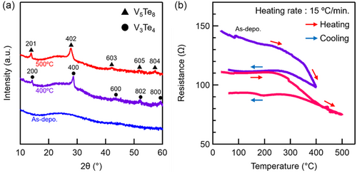
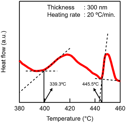
Figure 1a shows the X-ray diffraction (XRD) patterns of the as-deposited and annealed VTe thin films. The as-deposited film was identified as an amorphous phase, exhibiting no discernible diffraction peaks. Upon annealing up to 400 °C, the film exhibited a phase change from the amorphous to the V3Te4 phase, which was characterized by its distinct diffraction pattern. Further annealing to 500 °C resulted in the emergence of the V5Te8 phase, which indicates a sequential crystalline polymorphic phase change. As shown in Figure 1b, the temperature dependence of the electrical resistance provides further insights into the phase-change dynamics. The purple line represents the resistance (R)–temperature (T) curve of the as-deposited film when heated up to 400 °C followed by cooling down to room temperature, while the red curve represents the R–T curve of the 400 °C preannealed film when heated up to 500 °C followed by cooling down to room temperature. The as-deposited film exhibited an initial resistance of ≈150 Ω at room temperature (near 25 °C). As the temperature increased to 400 °C, the resistance decreased due to the phase change from the amorphous phase to the V3Te4 phase, which indicates the improved conductivity of the crystalline phase. Subsequent heating to 500 °C resulted in a further resistance reduction, which is attributed to the formation of the V5Te8 phase. After cooling down to room temperature, the final resistance stabilized at ≈90 Ω, which represents an overall reduction of ≈60 Ω from the initial value. These curves reveal that the change in resistance between the amorphous and crystalline states is relatively small. This limited resistance contrast suggests that the read accuracy of the memory may be constrained. The differential scanning calorimetry (DSC) analysis of the as-deposited film (Figure 2) revealed two distinct exothermic peaks during heating. As shown, the first peak begins at ≈400 °C and corresponds to the crystallization of the amorphous phase into the V3Te4 phase, and the second peak begins at ≈445 °C and indicates the phase change from V3Te4 to V5Te8. These findings further support the XRD findings, thereby confirming the sequential nature of the phase change from the amorphous to stable crystalline phase (V5Te8) via a metastable crystalline phase (V3Te4).
2.2 Microstructural Characterization
As shown in Figure 3, the microstructure of the annealed VTe thin films was examined through cross-sectional transmission electron microscope (TEM) observations. The bright-field microscopy image of the film annealed at 400 °C (Figure 3a) reveals a dense microstructure with a smooth surface and no delamination between the substrate and the thin film, which is advantageous in terms of device fabrication. The diffraction pattern of the film annealed at 400 °C (Figure 3b) confirms the formation of the V3Te4 phase, with no preferential crystalline orientation, which indicates an isotropic growth. High-resolution TEM (HRTEM) image and the inset inverse Fast Fourier transformation (IFFT) image shown in Figure 3c, which were derived from the FFT pattern obtained through HRTEM, provide direct evidence of the V3Te4 crystal lattice, thereby further validating the phase identification.
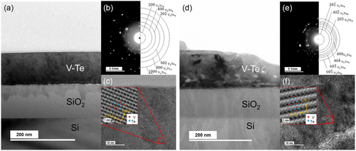
Similarly, the microstructure of the film annealed at 500 °C (Figure 3d–f) demonstrates the formation of the V5Te8 phase. This phase also exhibits isotropic growth, as demonstrated by the lack of preferential orientation in the diffraction pattern. The HRTEM image and the inset IFFT image clearly resolve the V5Te8 lattice, thereby confirming its crystallinity. Note that the TEM observation results also demonstrate that the VTe film exhibits a phase change from an amorphous phase to a stable V5Te8 phase via the V3Te4 phase by the annealing process.
2.3 Electrical and Optical Properties
Table 1 summarizes the corresponding Hall measurement results. As can be seen, the VTe thin film exhibits unique electrical properties. Unlike conventional amorphous materials that typically exhibit high resistivity and poor carrier mobility and carrier density, the amorphous VTe phase exhibited a remarkably low resistivity of 3.39 × 10⁻⁴ Ω, a relatively high carrier mobility of 0.368 cm2 V−1 s−1, and a carrier density of 5.00 × 1022 cm−3. This behavior is possibly attributed to the presence of transition-metal (vanadium in this study) clusters that introduce electronic states near the valence band, thereby enhancing the carrier generation and reducing the energy gap for excitation, as reported in previous PCMs, e.g., NbTe4 or Cr2Ge2Te6.[17, 31-33] These properties distinguish VTe from standard phase-change materials that exhibit a high-resistance amorphous phase, e.g., GST (Ge2Sb2Te5).
| VTe | GST (Ge2Sb2Te5)[36-38] | MnTe[24, 39, 40] | ||||||
|---|---|---|---|---|---|---|---|---|
| As-deposited | 400 °C annealed | 500 °C annealed | As-deposited | >≈155 °C | >≈365 °C | As-deposited | 500 °C annealed | |
| Phase | Amorphous | V3Te4 crystalline | V5Te8 crystalline | Amorphous | FCC crystalline | HCP crystalline | β phase crystalline | α phase crystalline |
| Resistivity [Ω cm] | 3.39 × 10⁻⁴ | 2.51 × 10⁻⁴ | 2.27 × 10⁻⁴ | ≈103 | ≈10−2 | ≈10−3 | 9.37 × 10² | 0.182 |
| Carrier density [cm−2] | 5.00 × 10²² | 3.48 × 10²² | 4.98 × 10²² | ≈1018 | ≈1020 | ≈1020 | 6.78 × 10¹⁵ | 1.05 × 10¹⁹ |
| Mobility [cm2 V−1 s−1] | 0.368 | 0.715 | 0.520 | ≈10−3 | ≈2 | ≈50 | 0.982 | 3.25 |
| Bandgap [eV] | 0.07 | 0.12 | 0.16 | 0.7 | 0.5 | 0.5 | 2.50 | 1.48 |
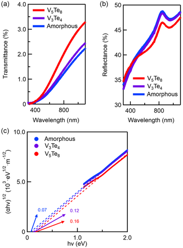
Here, d denotes the film thickness, T denotes the transmittance, and R denotes the reflectance.
Here, h denotes the Plank constant, v denotes the frequency, and A is a proportional constant. The value n, which is 2 or 1/2, is employed to determine the indirect and direct transitions, respectively. Figure 4c shows the Tauc plot of (αhv)1/2 as a function of hv for the thin film, indicating an indirect transition. The optical bandgaps of the amorphous, V3Te4, and V5Te8 phases were ≈0.07, 0.12, and 0.16 eV, respectively. These results demonstrate that the optical bandgap increases in the following order: amorphous phase, V3Te4 phase, and V5Te8 phase; however, it is important to note that all phases generally exhibited relatively small optical bandgaps.
2.4 Comparison with Other PCMs
Table 1 compares the physical properties of the VTe films with MnTe and GST.[28, 36-40] Unlike MnTe films, which typically exhibit a metastable β phase in the as-deposited state, the VTe films exhibit an amorphous phase in the as-deposited state. The difference may arise from variations in the deposition conditions, e.g., the sputtering pressure, gas composition, and targets.[41-43] However, the VTe amorphous phase exhibits considerably lower resistivity compared with the amorphous phase of GST, which may imply the presence of transition-metal clusters. The resistance and optical changes associated with the phase change in the VTe films are less than those observed in MnTe and GST, which may limit their use in applications that require a large resistance contrast. In particular, the phase change from an amorphous phase to a metastable crystalline phase (i.e., the V3Te4 phase) followed by a stable crystalline phase (V5Te8 phase) in the VTe thin films was similar to the order of the phase change in GST (amorphous phase → metastable face-centered cubic (FCC) phase → stable hexagonal close-packed (HCP) phase); however, as shown in Table 1, the changes in the electrical and optical properties upon phase change were much smaller in the VTe thin films.
2.5 Memory Device Performance
In this study, a contact-hole PCRAM device with a 200 nm diameter was fabricated (Figure 5a) to perform a practical evaluation of the applicability of the VTe film in-memory devices. The current–voltage (I–V) characteristics of the device, as shown in Figure 5b, indicate a clear resistance change during the current sweep. Here, the initial cell resistance was ≈685 Ω at 10 mA, which was found to decrease with increasing current, reaching a final value that was ≈98 Ω. This change corresponds to the phase change from the amorphous to the V3Te4 and V5Te8 phases, as driven by Joule heating. Figure 5c presents the resistance–voltage (R–V) characteristics of the memory device. In this experiment, the memory cell was first crystallized (set state) using a current sweep. Subsequently, voltage pulses with a pulse width of 100 ns were applied to the cell. As shown in Figure 5c, the cell transitions to a high-resistance amorphous state (Reset) at ≈5.6 V. Following this, the cell switches back to the low-resistance crystalline state (Set) at 6.2 V. This behavior suggests that the VTe-based memory exhibits reversible resistance switching. The consistency between the resistance changes in the memory device and the standalone films confirms that the phase-change behavior of the VTe film is preserved in the device structures; however, the relatively small resistance contrast indicates that the VTe film is not suitable for PCRAM devices. In addition, in the VTe film, no significant change in the carrier density upon the phase change was observed, thus, no change in device resistance due to change in the contact resistance between the VTe film and electrode would be expected. Other polymorphs can be found in other composition ranges of the VTe binary phase diagram; therefore, it may be worthwhile to investigate the effect of the composition on the phase-change behavior in VTe films for phase-change device applications.

3 Conclusion
This study investigated phase-change behaviors of VTe thin films with a composition of V:Te ≈ 0.4:0.6. The findings indicate that the amorphous phase exhibited unusually low resistivity and high carrier density, which is possibly attributed to vanadium cluster formation, thereby distinguishing it from conventional phase-change materials. In addition, the VTe film exhibited a phase change from an amorphous phase to a stable V5Te8 phase via the V3Te4 phase through the annealing process. The resistance changes during the phase changes in the VTe film were much smaller compared with MnTe and GST, which makes it difficult to apply the VTe binary system to PCRAM devices.
4 Experimental Section
Preparation of VTe Thin Film
The VTe films were deposited on SiO2 (100 nm)/Si (625 μm) or glass (Corning EAGLE XG) substrates by radio frequency (RF) magnetron co-sputtering of V (99.9%; TOSHIMA Manufacturing Co., Ltd.) and Te (99.99%; Kojundo Chemical Laboratory Co., Ltd.) pure targets at room temperature (300 K) in an Ar gas atmosphere. The base pressure of the chamber was less than 5.0 × 10⁻⁵ Pa, and the working pressure was ≈0.6 Pa. The thickness of the VTe thin film was measured by atomic-force microscopy (KEYENCE, VN-8000). The as-deposited film with a thickness of 100 nm was annealed to 350 °C (heating rate: 15 °C min−1) and cooled down to room temperature in the Ar gas atmosphere in a furnace.
Characterization of VTe Thin Film
The composition of the VTe thin film was determined by scanning electron microscopy (SEM) and energy-dispersive X-ray spectroscopy (Fe-SEM, JEOL, JSM-6500 F), and the V:Te ratio was 44:56. The VTe films (thickness: 1 μm) used for composition analysis were deposited onto a SiO2 (100 nm)/Si (625 μm) substrate. The crystal structures of the as-deposited films and annealed films were measured by XRD (Rigaku, Ultima IV). The X-ray source was Cu–Kα, and the diffraction patterns were measured in the range of 20°–60° using the 2θ/θ method. The films (thickness: ≈100 nm) for XRD measurement were deposited onto a glass substrate. The temperature dependence of the electrical resistance of the VTe films was measured using a two-point probe in the annealing furnace. In addition, the electrical properties of the film were investigated by Hall-effect measurement (Toyo Corp., ResiTest 8400). The films (thickness: ≈100 nm) used for the Hall-effect measurement were deposited onto a glass substrate. The optical properties of the film were measured using a spectrophotometer (JASCO Corp., V-730). To investigate whether a phase change occurred in the VTe thin film, thermal analysis was performed using a differential scanning calorimeter (DSC, TA Instruments, Q20). Here, the sample film thickness was 300 nm, and the temperature increase rate was 20 °C min−1. The cross-sectional microstructure observation was performed on the VTe thin films using TEM (JEOL, JEM-2100 F) at an accelerating voltage of 200 kV. The TEM samples were thinned by ion milling (Gatan, PIPS Model 691).
Memory Device Fabrication
The memory device fabricated in this study was a contact-hole type memory device structure. Here, a tungsten bottom electrode (50 nm) was deposited on a SiO2 (100 nm)/Si (625 μm) substrate after photolithography, and a SiO2 insulation layer (100 nm) was deposited on top of the tungsten bottom electrode negative resist (ZEON Corp., ZPN 1150-90) was used as the photoresist. Contact holes (diameter: ≈200 nm) were drilled on the SiO2 insulating layer using a focused ion beam until they reached the bottom electrode. The VTe layer (150 nm), i.e., the memory layer, was deposited over the contact holes, and a tungsten top electrode (200 nm) was deposited in situ in the same sputter chamber to avoid unwanted oxidation of the memory layer.
Memory Device Characterization
The I–V sweep for all devices was measured using a semiconductor parameter analyzer (Keysight, B1500A).
Acknowledgements
This work was supported by the JSPS KAKENHI (grant nos. 21H05009 and 24K21668). This work was supported in part by the Commissioned Research (grant no. JPJ012368C03701) of the National Institute of Information and Communications Technology (NICT), Japan. The authors acknowledge the financial support from the JST FOREST Program, grant no. J240002622, and the Nippon Sheet Glass Foundation for Materials Science and Engineering (NSG Foundation). The authors thank Dr. T. Miyazaki (Tohoku University, Japan) for his technical support for the TEM measurements.
Conflict of Interest
The authors declare no conflict of interest.
Author Contributions
Shuhei Oihara: formal analysis (lead); investigation (lead); visualization (lead); and writing—original draft (lead). Yi Shuang: funding acquisition (lead); investigation (supporting); supervision (equal); and writing—review editing (lead). Daisuke Ando: formal analysis (equal) and investigation (supporting). Yuji Sutou: conceptualization (lead); formal analysis (equal); funding acquisition (lead); project administration (lead); supervision (lead); and writing—review editing (equal).
Open Research
Data Availability Statement
The data that support the findings of this study are available from the corresponding author upon reasonable request.


