Dynamic Multi-Focus 3D Laser Nanoprinting Based on Two-Step Absorption and Computational Holography
Abstract
Two-step-absorption 3D laser nanoprinting allows for using compact and low-cost continuous-wave (cw) lasers. Therefore, it is an attractive alternative to established state-of-the-art multi-photon-absorption 3D laser nanoprinting. Additionally, low single-focus polymerization-threshold laser powers pave the way for multi-focus parallelization approaches while still using compact cw laser sources. Parallelization is further encouraged by the fact that single-focus scanning velocities are inherently limited by the intermediate-state lifetime of the photoresist system used. Herein, a 3D nanoprinting setup that combines an established two-step-absorption photoresist system with a dynamic multi-focus approach based on binary holography and a digital micromirror device (DMD) is presented. The generated holographic patterns allow for combined beam-splitting and beam-steering as well as for the control of each focus’ individual intensity. Therefore, one obtains a versatile printing approach, enabling a dynamic change of the number of foci for each pattern, based on the structure to be printed. With this setup, the printing of 3D microstructures using up to 31 laser foci in parallel at a print rate of up to is achieved. Additionally, the capabilities and limits of the chosen approach are compared with rate-equation calculations.
1 Introduction
The field of 3D laser micro- and nanoprinting[1, 2] constantly innovates printing technologies and their applications. Current research efforts strive to widen the application topics and further develop the technology,[3-5] by making it faster,[6-9] increasing spatial resolution,[10, 11] and making more dissimilar materials available for 3D printing.[12-14] Many approaches of 3D laser micro- and nanoprinting utilize two- or multi-photon absorption processes.[1] However, alternatives are emerging.[4, 15] Among those alternatives is two-step absorption.[16-20] Two-step-absorption 3D laser nanoprinting allows for the use of compact low-cost continuous-wave (cw) laser sources. Here, we take advantage of these low-power single-focus polymerization thresholds to parallelize one-color two-step-absorption 3D printing using digital holography in order to address the urgent need for higher print speeds in 3D printing.
3D laser printing relies on the absorption of photons by a photoinitiator molecule, which generates radicals and thereby starts a radical polymerization reaction. To confine this reaction in space and suppress unwanted dose accumulation, a nonlinear relation of polymerization dose and light intensity is needed.[1] This can be provided by an optical nonlinear two-photon absorption. This process, however, requires large light intensities and therefore relies on pico- or femtosecond pulsed lasers. As an alternative, we have previously introduced and demonstrated 3D printing using two-step absorption.[16] Hereby, the sequential absorption of two photons via a real intermediate state leads to an effective optical nonlinearity. Due to the finite lifetime of this intermediate state, single-focus laser powers have been well below and the use of compact and cost-efficient cw lasers is feasible.[16] On this basis, a compact shoe-box sized 3D laser nanoprinter has recently been realized.[18] Furthermore, by carefully selecting the photoinitiator molecule, the absorption spectra of the two sequential absorptions can be tuned. This allows for a rich behavior of photoinitiation mechanisms. Additional to one-color two-step absorption, a second wavelength can introduce depletion mechanisms,[17] enabling enhanced printing resolution. Besides this, non-overlapping absorption spectra of the ground state and the intermediate state enable two-color two-step absorption, which allows for massive parallelization by light-sheet 3D microprinting.[19]
There are several possibilities for increasing print rates and thereby lowering overall print times in 3D laser micro- and nanoprinting. When scanning a focused laser beam throughout the volume, i.e., polymerizing one voxel at a time, print rates can be increased by increasing the focus scan velocity. Additionally, parallelization efforts can be undertaken, increasing the number of voxels polymerized at a time. This includes multi-focus approaches,[6, 9, 21-23] projection approaches of 2D planes[19, 24-27] as well as volumetric additive manufacturing approaches.[26, 28-30] Determining which approach provides the largest benefits largely depends on the photoinitiation mechanism used and the laser power available. Considering a photoinitiation process with an effective nonlinearity exponent of , doubling the focus scan velocity doubles the print rate, but increases the necessary laser power only by a factor of . Therefore, at a fixed nonlinearity, an increase of the focus scan velocity up to technological limits is advantageous.[6] However, in photoresist systems featuring two-step absorption, the effective nonlinearity depends on the focus scan velocity.[16] This property is connected to the finite lifetime of the intermediate state of the photoresist system. When approaching focus scan velocities, and therefore exposure times, in the regime of the intermediate-state lifetime, the effective nonlinearity exponent decreases when going to faster focus scan velocities. This not only lowers the power scaling argument, but, more importantly, it also decreases the printing quality. Therefore, parallelization approaches are a valid avenue for increasing print rates in two-step-absorption photoresist systems with no need of pushing focus scan velocities up to technological limits.
Here, we report on a parallelization approach for one-color two-step-absorption 3D printing based on an established photoresist system comprising benzil as photoinitiator.[16] We start by discussing the application of binary holography using a digital micromirror device (DMD) as the parallelization method chosen. Following this, we describe the dedicated optical setup for 3D printing as well as the printing principle in more detail. This is discussed by illustrating the procedure of transferring a 3D design to a set of digital holograms prior to printing. Thereafter, we present a gallery of 3D printed structures as performance tests. Finally, we discuss different printing strategies and their particular influence on two-step-absorption photoresist systems and compare them with dose simulations based on rate-equation calculations.
2 A Printing Setup Based on Computational Holography for Two-Step-Absorption 3D Printing
2.1 Design of the Printing Setup
2.1.1 Discussion of Multi-Focus Approaches for Two-Step 3D Laser Nanoprinting
When printing with more than one laser focus at a time, there are several approaches for beam-splitting and beam-steering. These can be categorized into static and dynamic approaches. Static beam-splitting approaches feature a fixed focus pattern, which is scanned across the print field using additional devices. Creating static multi-focus patterns by diffractive optical elements,[9, 31] refractive multi-lens arrays,[22, 32] or a combination thereof[6] offers high power efficiencies. Such static approaches reach their full advantage for power-critical applications where the fabrication of many identical structures or large periodic structures is desired.[6] Two-step-absorption 3D printing initially uses low single-focus laser powers below and is, due to the chemistry of the photoresist system, well suited for fast printing of rather small volumes exhibiting high resolution.[16]
Therefore, we concentrate the discussion around dynamic approaches. Dynamic approaches offer the possibility of changing the multi-focus pattern during printing. Additionally, the beam-steering of the respective foci can be accomplished by the dynamically changing focus pattern, therefore dispensing of a separate beam-steering device. As a simple implementation, one could think of the direct imaging of displays to the print plane. When generating sparse multi-focus patterns however, only a very small fraction of the light is guided to the print plane, rendering the power efficiency very low.[33] Increasing the number of activated pixels also poses certain limitations, since interference effects of foci become stronger when decreasing the distance of neighboring foci.[9, 21, 34]
An alternative to direct imaging a display is to place a spatial light modulating device in the Fourier plane of the microscope-objective lens.[21, 23, 26, 33, 35-39] The device modulates the amplitude and/or phase of the incoming wave such that it creates the desired multi-focus pattern behind a Fourier-transforming lens. Therefore, a larger fraction of the light is redistributed towards the foci instead of being lost in a beam dump.
The choice of the device often comes down to the choice between phase-modulating spatial light modulators (SLMs) and binary amplitude-modulating DMDs. Phase holograms generated by SLMs allow for a better power efficiency since the diffraction patterns’ zeroth order can be effectively suppressed.[39-41] Binary amplitude holograms come with the disadvantage of a strong zeroth order, which must be blocked for printing.[21, 41] On the other hand, DMDs feature high patterning rates in the kHz range and are typically more cost-efficient, since they are produced at large numbers.[42] We reiterate that two-step-absorption 3D printing features low single-focus laser powers. Then, when compared to two-photon absorption, a lower power efficiency of the parallelization technique can be more easily compensated for by higher power laser sources. Additionally, two-step absorption is well suited for printing structures with low filling fractions. Therefore, and in combination with the limitation of interference effects of foci in close proximity, it is more advantageous to be able to faster change the pattern while using a lower number of foci within each pattern. We want to emphasize that the patterning rates employed when using either SLMs or DMDs are both in the nonlinear regime of the photoresist system,[16] therefore not contradicting the prior discussion on the power scaling.
Both phase holography using SLMs as well as binary amplitude holography using DMDs have previously been implemented for several beam-splitting and beam-steering tasks. These include applications in the field of microscopy,[43, 44] optical tweezers,[45-47] as well as 3D laser microprinting using two-photon absorption.[21, 23, 26, 33, 35-39] For our presented implementation of parallelized two-step-absorption 3D laser nanoprinting, we opted for binary amplitude holography for the reasons discussed above.
2.1.2 Optical Setup
In Figure 1a, we show a scheme of the optical setup used for parallelized two-step-absorption 3D laser nanoprinting. As the laser source, we use a compact cw diode laser (Toptica iBeam smart) emitting laser light at center wavelength with a full-width-at-half-maximum (FWHM) of the emission spectrum of about . The maximum output power of the laser diode is . The laser beam is magnified to match the entrance pupil of a πShaper (AdlOptica πShaper 6-6) via a telescope consisting of the lenses L1 and L2. The πShaper transforms the circular, Gaussian-shaped intensity profile to a circular, but uniform intensity profile by using refractive optical elements. Following the πShaper, the beam is further expanded towards a blazed grating (, blaze wavelength). Since the diode laser used is emitting laser light at several longitudinal modes, there is a certain wavelength range present in the emission spectrum. Therefore, a blazed grating is placed into the beam path to pre-compensate for angular dispersion effects introduced by the diffraction of the pixelated surface of the DMD.[21] The blazed grating is positioned under a small angle to maximize diffraction efficiency as well as reducing the ellipticity introduced on the laser beam. The result is illustrated in Figure S3 (Supporting Information). Following the blazed grating, the laser beam is imaged and de-magnified onto the DMD surface (Texas Instruments DLP4500). The focal lengths of the lenses L5 () and L6 () are matched with the diffractive parameters of the blazed grating and the DMD to effectively pre-compensate for angular dispersion effects.[37]
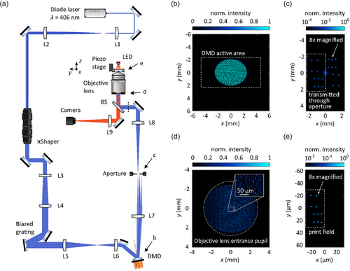
The DMD's active elements are small tiltable aluminum-based micromirrors with side length each, arranged in an array of .[48] Due to the small pixel size, the DMD effectively acts as a blazed grating itself, independent of the pattern displayed on the DMD. Therefore, the DMD is arranged such that the usable output intensity for printing is maximized. In doing so, the incident and the diffraction angle with respect to the mirror normal are not identical, adding a certain ellipticity to the output beam (see Note S2, Supporting Information).
The optical path following the DMD towards the print plane is further illustrated by simulations based on Fourier optics with paraxial approximations (Figure 1b-e).[24] In Figure 1b, we show the light intensity at a plane right after the DMD. The DMD displays a binary pattern which is multiplied with the incident wave. Here, as an example, we have chosen a holographic pattern which generates a focus distribution of 10 foci. This focus pattern can be seen in the Fourier plane of the DMD (Figure 1c). Besides a zeroth order, the designed focus pattern repeats in higher diffraction orders (only ±1st orders are shown). Via a rectangular aperture, only the +1st order is transmitted, as indicated by the white, dashed rectangle. At the entrance pupil of the objective lens (Figure 1d), the spatially filtered pattern displayed on the DMD is imaged. At this position, we measured the maximum available laser power for printing to be typically . Finally, in the print plane, the focus pattern transmitted through the rectangular aperture is imaged and de-magnified by using a high-numerical-aperture (NA) objective lens (Leica HCX PL APO 100×/1.4−0.7 Oil CS). The focus distribution in the print plane is shown in Figure 1e with the addressable print field indicated by the white, dashed rectangle. For better visibility, each focus’ diameter in the Figure 1c,e is shown 8× magnified.
To summarize the above, we start with output from the laser, of which about impinge onto the DMD and typically a measured enter the entrance pupil of the focusing microscope objective lens. Depending on the holographic pattern, this value of can change by about . This means that only about of the laser power is used for printing.
For in-situ monitoring of the printing process, the print plane is illuminated by a red-light LED (Thorlabs M625L4), the light is transmitted through the dichroic mirror (Thorlabs DMLP505) and imaged onto a CMOS camera (FLIR Blackfly S). Fine sample movement in -direction and therefore slicing of the structure is achieved by a piezoelectric inertia stage (PI Q-545.140). Using this piezoelectric stage, different printing layers are approached in a step-like manner. Coarse -positioning is accomplished via two linear screw-drive stages (Aerotech ATS50).
In the optical design of the setup, there are certain critical parameters. These include the maximum extent of the print field accessible without translating the sample. This parameter is directly connected to the minimum distance of neighboring voxels, a quantity commonly referred to as “hatching” in single-focus-scanning 3D laser printing. Additionally, the DMD's active area as well as the entrance pupil of the objective lens pose size restrictions. All these demands lead to the chosen trade-off. The beam diameter at the DMD is set to around in - and in -direction. With a chosen hologram resolution of , the DMD active area is . Therefore, no laser power is lost due to over-illumination of the DMD, however, not all pixels contribute to the light modulation. This effectively leads to a loss in uniformity of the focus pattern that we found to be acceptable (see Figure S4, Supporting Information). With focal lengths of the lenses L7 and L8 of and , respectively, the objective lens’ entrance pupil is slightly under-illuminated in -direction but over-illuminated in -direction. This is again set as a compromise between focus quality and power loss. Besides the beam diameter, the optics have also to be matched to the desirable scan range and step size. We choose the optics such that the maximum scan range in the print plane covers an area of . From the maximum scan range, however, only a print field of is used (see Figure 1e). The remaining area is either obscured by the point symmetric image of the focus pattern (see Figure 1c) or by additional focus patterns originating from different diffraction orders of the DMD's pixelated surface (see Figure S2, Supporting Information). Also connected to the maximum scan range is the minimum step size, which calculates to in - and in -direction.
2.2 From the 3D Model to the Set of Holograms
In the following, we explain the procedure of getting from a 3D print design to a set of holographic patterns displayed on the DMD. This discussion is split into a part on what we will refer to as printing strategy and a part on the calculation of the holograms.
2.2.1 Defining the Printing Strategy
The steps explained in the following are illustrated in Figure 2. As is common in 3D printing, we start with a 3D design, e.g., an *.stl file. This is first sliced into a number of 2D layers, applying a certain slicing distance. If not stated otherwise, we have applied a slicing distance of for the structures shown. Additionally, the 2D layers are matched to the discretization of addressable focus positions. In a next step, each 2D layer is further divided into a set of point patterns, as can be seen in Figure 2c. For this step, certain restrictions apply.
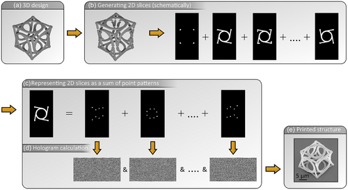
The fraction of the intensity diffracted into the 1st order has only a minor dependence on the holographic pattern and therefore on the focus pattern. That is why the number of foci illuminated in parallel at a fixed exposure time is limited by the available laser power. In our implementation, this limit is reached at a focus number of around 30. Additionally, the minimal distance between neighboring foci is limited to not suffer from detrimental interference effects of multiple foci. This limitation is reached at a focus-to-focus distance of a few µm.[21] Therefore, depending on the structure to be printed, the number of foci employed in parallel is often lower than the power-limited focus number. In Figure 2, this can be seen when looking at the first 2D layer exhibiting only 4 distinct features, where, due to focus spacing restrictions, only 4 voxels can be exposed in parallel. Another important aspect for optimizing the printing strategy is the temporal sequence, i.e., the foci can either follow a line-scanning approach or follow a random sequence. We will specifically address this aspect in Section 4. Additional details on the printing strategies chosen for the different structures shown can be found in Note S1 (Supporting Information). Since the various point patterns will cover an unequal number of points, the intensity carried by each focus will change. This can be compensated for by synchronously modulating the laser output power or by placing additional foci outside the print field which are blocked by the rectangular aperture. We have chosen the latter approach since there is no additional synchronization effort necessary.
2.2.2 Calculating the Holograms
Finally, from each individual point pattern, a hologram is calculated, as illustrated in Figure 2d. For the calculation of amplitude as well as phase holograms, a multitude of algorithms exist.[40, 47, 49, 50] Among the most common algorithms are iterative phase retrieval algorithms. Iterative algorithms allow for reaching high quality holograms translating into focus patterns of high uniformity. However, the computational time increases with the number of iterations.[40] The number of holograms to be calculated for our 3D printing approach reaches values in the order of . Therefore, the computation time is of concern and should be kept minimal. This is why we have chosen a direct instead of an iterative algorithm for the parallelized calculation of a large number of holograms.
The holographic pattern is given by the inverse Fourier transform of the desired point pattern in the print plane. To map this holographic pattern to the DMD's binary amplitude modulation, all pixels with phases between and are set to the “on” state and all other pixels are set to the “off” state.[40] These calculated holographic patterns, or binary amplitude gratings in this case, allow for a maximum power of diffracted into the +1st order.[51] The quality of the holograms and the accompanying focus patterns are slightly lower compared to iterative algorithms, however sufficient for our implementation (see Figure S4, Supporting Information). This is particularly the case since we are not relying on periodic focus arrays.[52] Therefore, the gain in computational time outweighs a small loss in focus uniformity.
After the computation, all binary holograms are assembled as images with a color depth of and put together as a video file for each printed structure. These video files are streamed from a PC to the DMD's controller chip via a HDMI connection. The DMD's controller chip again unpacks the images and displays a sequence of holograms. We use this approach to not be limited by the DMD's internal memory. We choose frame rates up to for the HDMI connection, resulting in a maximum patterning rate of , corresponding to an exposure time of per holographic pattern (see Figure S6, Supporting Information). Accompanying this video stream, the piezoelectric stage is used to move to different print planes inside the photoresist in a step-like fashion.
3 Dynamic Multi-Focus Printing of 3D Microstructures via Two-Step-Absorption Photoinitiation
Using the optical setup presented above, we have printed a variety of structures to evaluate the printing performance of our parallelized 3D laser nanoprinter. Since these structures impose different demands on the printing process, we have used different printing strategies. We will expand on this as well as the accompanying capabilities and limits of our printing approach in more detail.
In Figure 3, we show scanning-electron micrographs of different structures. Detailed printing parameters of all the structures are provided in Table S1 (Supporting Information). Figure 3a shows the result of printing 15 trefoil knot structures simultaneously employing up to 31 foci in parallel. As already discussed above (cf. Section 2.2.1), due to the restriction of a minimum distance between neighboring foci, the number of foci per hologram varies, which is why we always state the maximum focus number employed for printing for each structure. The laser power used for printing is set to per voxel. Each knot structure has lateral dimensions of and a height of such that the shown 15 trefoil knots span almost the entire print field as discussed in the previous section. The total print time of the structures is , which results in a print rate of . For the print rate, each point of the point patterns employed is calculated as one voxel. This is justified by the fact that with every single hologram, entirely different and independent point patterns can be exposed. Therefore, the total number of points which make up one structure is divided by the total print time to calculate the print rate in terms of the number of . Hence, the stated print rate is a mean print rate for the particular structure and comprises effects such as the dark periods during printing as well as run-up times or settling times of devices used in the setup, whenever needed. By this discussion, an advantage of the used dynamic multi-focus approach using DMDs in comparison with, e.g., focus-scanning approaches using galvanometric mirrors can be seen. Because of their moments of inertia, the latter often need run-up times to reach the best printing results.[7] Even though DMDs also contain moving mechanical parts, i.e., the aluminum-based micromirrors, they are very small and lightweight. Settling times of the micromirrors are in the range of a few microseconds[46, 48] and therefore around two orders of magnitude smaller than the exposure times of each single hologram.
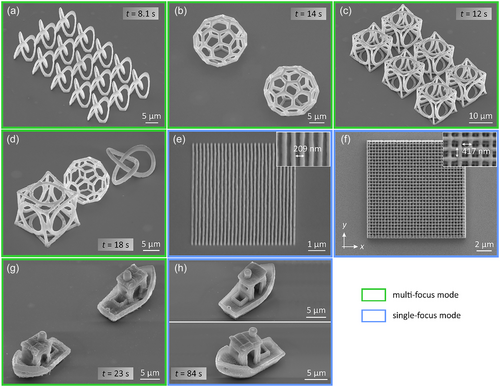
Further 3D test structures are shown in Figure 3b–d. In b, we show the result of printing two diameter buckyball structures in . These were printed using up to 8 foci in parallel, resulting in a print rate of . Panel c shows the printing of six unit cells of a chiral metamaterial structure,[53] printed in using up to 24 foci in parallel (). To pre-compensate for proximity effects, a grayscale exposure profile has been applied following the approach described in ref. [19]. Therefore, the relative intensities of the different foci within one exposure are varied. This decreases the intensity in dense regions, to avoid detrimental proximity effects. To further demonstrate the full freedom of our dynamic multi-focus printing, Figure 3d shows the parallel printing of entirely different structures. These three structures were printed in with up to 15 foci in parallel. However, due to the different heights of the three structures, the number of foci employed decreases in the upper layers to still maintain a minimum focus distance.
The structures discussed so far have all been printed using multiple foci in parallel, where the number of foci and therefore the printing strategy were adjusted to the specific structure. To assess the printing resolution of our parallelized two-step-absorption printing setup, we printed 2D line gratings as well as 3D woodpile structures. These are shown in Figure 3e,f. In both cases, the structures were printed using a single focus at a time to exclude effects related to the number of foci. Line gratings were printed with line-to-line distances of and woodpile structures with lateral periods of . All of these are still well resolved. These results show a slightly worse resolution than our previous results on two-step-absorption 3D laser nanoprinting employing single-focus scanning.[16, 18] We attribute this difference to the larger focus dimensions since the objective lens’ entrance pupil is not fully filled in one lateral direction. Additionally, each focus comprises several side maxima as well as higher diffraction orders as it is expected from the illumination profile of the objective lens’ entrance pupil. As already discussed in Section 2, this is partly the result of a compromise between laser power efficiency and printing resolution and partly inherent to binary amplitude holography. Measurements of the focus quality can be found in Figure S5 (Supporting Information). Additionally, we should like to recall the minimum step sizes of neighboring foci as already mentioned in Section 2. These are limited to around and in both lateral dimensions, therefore also discretizing the minimum line grating and woodpile periods. In terms of minimal steps, or pixels in the calculation of the holograms, the line grating shown in Figure 3e has a line-to-line distance of . The woodpile structure (Figure 3f) was calculated with periods of in the - and in -direction. We should like to mention that although the are the minimum step size achievable with the presented setup, different step sizes can be achieved when changing the number of pixels of the holographic pattern.
Finally, Figure 3g,h shows the printing result of a #3DBenchy,[54] a common test structure in 3D printing. This is particularly challenging due to its large filling fraction while, at the same time, containing fine features. Here, we show a comparison of printing with multiple foci in parallel (Figure 3g) and with a single focus at a time (Figure 3h). In Figure 3g, two boats are printed in parallel using up to 15 foci in a total print time of . Compared to this, a single boat was printed using 1 focus at a time in . As can be seen from the scanning-electron micrographs, the boat printed in the single-focus mode exhibits better printing quality with less severe proximity effects present. This is especially apparent when looking at the cabin, which is nicely reproduced in the single-focus mode, however over-polymerized in the multi-focus mode. Here, the limits of our parallelized 3D laser nanoprinting approach in combination with the two-step-absorption photoresist system become apparent. As already known,[16] structures of high filling fractions are challenging for two-step-absorption photoresist systems. An essential ingredient to the photoresist system is the quencher molecule which maintains the necessary nonlinearity for 3D printing. The results, however, indicate that these molecules are (partly) consumed during the printing process, therefore diffusion processes are needed to again increase the local quencher concentration. This aspect poses certain limits in terms of the exposed volume per unit time. Nevertheless, since the number of foci employed in parallel is tunable, an adaption of the printing strategy matching the specific characteristics of the structure to be printed as well as the photoresist used is readily possible.
4 Spatiotemporal Proximity Effects in Two-Step-Absorption 3D Laser Nanoprinting
In this section, we discuss the influence of the temporal sequence of exposures on the printing result. This discussion is mainly motivated by two factors: 1) the finite lifetime of the intermediate states and the reaction-diffusion kinetics involved in the printing with two-step-absorption photoresists and 2) the parallelization approach of computational holography that creates more freedom regarding the temporal sequence, since adjacent holograms can address completely different focus positions without restrictions due to, e.g., run-up times of beam steering devices.
Figure 4a,b shows an illustration of two different temporal sequences for the example of a square plane of side length. In Figure 4a, each point of the square is exposed following the neighboring point, similar to a line scan using, e.g., galvanometric mirrors for beam steering. We refer to this setting as an ordered focus distribution. In contrast, using the random focus distribution, the points making up the square structure are exposed in a random order. Figure 4c,d shows scanning-electron micrographs of printed square structures using the two presented printing strategies. We should like to emphasize that the set of holograms displayed for printing are the same in both c and d, only the temporal sequence is different. However, the printing results are different, too. While the ordered focus distribution leads to a rather uniform surface, the random focus distribution gives rise to a non-uniform surface with many hills and valleys. Additionally, especially at the edges, the single exposures can be seen as disconnected polymerized voxels. Overall, the random focus distribution shows less polymerized volume (using the same laser power of ) compared to the ordered focus distribution.
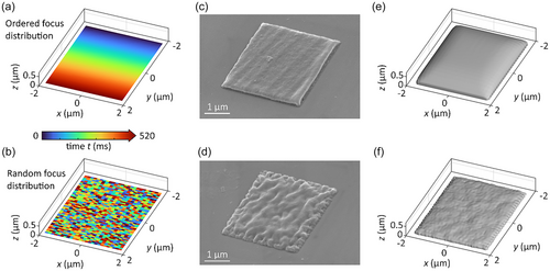
In terms of a simple accumulation model for calculating the exposure dose and therefore proximity effects, the temporal sequence makes no difference on the printing result.[55] This simplification often leads to adequate results for two-photon absorption 3D laser printing. However, temporal effects do matter when looking at long exposure times and/or fine features.[56, 57] For two-step-absorption photoresists, spatiotemporal proximity effects play an important role in a wide range of printing conditions.[16, 19] Therefore, we have performed calculations simulating the printed structure based on a rate-equation approach. The results are depicted in Figure 4e,f. These simulations take the different printing strategies of ordered and random focus distributions into account and show a qualitative agreement with the experiment. For the rate-equation model, we built on previous work.[16, 19] Details can be found there as well as in Note S5 (Supporting Information). The rate-equations model the reaction scheme of the two-step photoinitiation process. This takes the finite lifetime of the intermediate state (on the order of tens of microseconds) as well as quenching and scavenging processes into account. To arrive at reasonable computation times, we approximate the spatial diffusion processes of the photoinitiator molecules and the quencher molecules by effective time constants (as in ref. [19]). The corresponding rates also cover the regeneration of the population of the photoinitiator initial states as well as of the quencher within the reaction volume. It has been found that the combination of all of the mentioned processes is important to accurately model spatiotemporal proximity effects in two-step-absorption 3D printing.
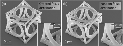
On this basis, the printing strategies for 3D structures can be adapted to increase the printing quality. As an example, Figure 5 shows scanning-electron micrographs of two structures printed with different temporal sequences of the holograms. Both were printed using a single-focus mode. In Figure 5a, however, an ordered focus distribution has been employed while in panel b a random focus distribution (within each layer) is used. As for the structures shown in Figure 4, the random focus distribution (Figure 5b) leads to a grainy surface of the printed structure. With this, the temporal sequence is another restriction which must be considered when calculating the set of holograms (cf. Section 2.2.1).
5 Discussion
In this section, we compare the results described above with those of other laser-based 3D printing approaches and describe possible future improvements of the underlying apparatus.
Our comparison is based on the overview chart printing speed versus voxel size of which we have published several generations throughout recent years.[9, 4, 6, 5] The most recent version is published on our website.[58] The printing rates described above range from to . Many of the voxel sizes quoted in [58] have been deduced from the FWHM of the squared intensity profile of the laser focus point spread function. Specifically, the voxel size refers to the mean of the lateral and the axial FWHM. For our conditions the lateral FWHM is , the axial FWHM is , and the resulting voxel size is , as obtained from calculations using the modified Richards & Wolf integrals.[59]
We start by comparing our results using two-step absorption with other results out of the broader class of (1+1)-photon absorption processes.[4] The print rate of is larger than that of all other one-color (1+1)-photon processes. It falls behind the print rate of of two-color two-step absorption using a light-sheet approach.[19] That approach used 33000 independent foci, i.e., a much larger number than the largest number of 31 foci used in the present study. While both studies use continuous-wave lasers, ref. [19] used a total laser power of about , which is 75 times more than in the present study. Furthermore, the experimental complexity of the light-sheet approach is much larger. We will come back to possible improvements of our approach below.
Next, we compare our results with those of two-photon absorption. There, more than a thousand times larger print rates of about have been achieved.[6, 58] Commercial instruments (e.g., Nanoscribe Photonics Professional GT) have been operating at print rates of for many years already. At present, our approach cannot compete with this performance. However, to be fair, these instruments are based on costly femtosecond lasers rather than inexpensive cw lasers.
Finally, parallelized one-photon absorption approaches have recently also made substantial progress.[8] They achieved a print rate of at a voxel size of . The voxel size in the present paper is about 8 times smaller, the print rate is more than two orders of magnitude slower.
This brings us to a discussion of possible next technological steps within our approach in regard to simplifications and increasing the print rate to surpass existing commercial femtosecond two-photon-absorption-based printers. We see five major points. First, the grating used to compensate the angular dispersion introduced by the DMD could be eliminated provided that a sufficiently powerful narrow-band cw laser is available. Second, the πShaper could be eliminated. In this case one would have to compensate the uneven intensity profiles of the different foci in the print plane via the holographic patterns. However, this step requires significantly increased computational effort, possibly a larger number of DMD pixels, and leads to a certain loss of laser power. Third, the piezoelectric -stage could be eliminated. The scanning of the -position of the foci could also be taken over by the holographic patterns — again at the cost of increased computational effort.[21] However, one would still need a possibility to position the substrate at a predefined -position before starting the printing process. Fourth, the voxel size could be adapted on-the-fly by correspondingly calculated holographic patterns to mimic two-photon grayscale lithography and to smoothen surfaces. However, one needs a reliable model for the photoresist response in order to pre-calculate these patterns to achieve a desired object. As we have seen in our above discussion on the spatiotemporal proximity effect, arriving at such a model for two-step absorption is not trivial. Fifth, the binary-amplitude-modulating DMD used in our work could be replaced by phase light modulators that may soon become commercially available at comparable cost.[60] Such phase modulators would enable a much better suppression of the zeroth order of the diffraction pattern which would enable a larger number of foci, thereby potentially increasing the speed of parallelized one-color two-step-absorption 3D printing.
6 Conclusion
Parallelization as a means for increasing print rates is especially attractive in two-step-absorption 3D laser nanoprinting, since low single-focus laser powers allow for multi-focus approaches still using compact cw laser sources. In this work, we have presented a dynamic multi-focus approach for two-step-absorption 3D laser nanoprinting. It is enabled by binary amplitude holography using a digital micromirror device. With this approach of parallelized one-color two-step-absorption 3D printing, we are bridging the gap between previous implementations of two-step-absorption 3D laser micro- and nanoprinting.[16, 18, 19] We have reported on the design and the implementation of our 3D laser printing setup, as well as shown the 3D printing capabilities of our approach by printing standard test structures. In doing so, we have addressed certain limitations that are special to two-step absorption. Furthermore, we have discussed the importance of spatiotemporal proximity effects in two-step-absorption 3D laser printing by comparing experimental results with rate-equation calculations. Finally, we have identified several possible future improvements of our approach.
7 Experimental Section
Photoresists
The used photoresists follow the description of PR1 and PR3 in ref. [16]. Both photoresists contain of the photoinitiator Benzil (, Aldrich) and of the molecule BTPOS (bis(2,2,6,6- tetramethyl-4-piperidyl-1-oxyl) sebacate, , TCI Chemicals). These were mixed into of the monomer PETA (pentaerythritol triacrylate, PR1) or TMPTA (trimethylolpropane triacrylate, PR3). PETA was purchased from Sigma-Aldrich. TMPTA () was purchased from Alfa Aesar. The mixture was stirred on a hotplate for . During the first , the mixture was heated to .
Sample Preparation and Development
For all samples, a diameter ring of polydimethylsiloxane (PDMS) ring was placed on a methacrylate silanized glass coverslip (no. 1.5H, Paul Marienfeld). A droplet of of the photoresist is contained in this ring. All samples were developed for in acetone (spectroscopy grade) and subsequently washed for in 2-propanol (spectroscopy grade). Afterwards, the samples were then blow-dried in a stream of nitrogen.
Acknowledgements
The authors acknowledge funding by the Deutsche Forschungsgemeinschaft (DFG, German Research Foundation) under Germany's Excellence Strategy for the Excellence Cluster “3D Matter Made to Order” (2082/1–390761711), by the Carl Zeiss Foundation through the “Carl-Zeiss Foundation-Focus@HEiKA”, and by the Helmholtz program “Materials Systems Engineering”.
Open access funding enabled and organized by Projekt DEAL.
Conflict of Interest
The authors declare no conflict of interest.
Open Research
Data Availability Statement
The data that support the graphs and simulations in this study are published in the open-access data repository of Karlsruhe Institute of Technology (https://doi.org/10.35097/rswzke266nhqd0ze).


