High Performance Electrically-Injected InGaN Microdisk Lasers through Simultaneous Enhancement of Optical Confinement and Overlap Factor
Abstract
Despite the considerable research interest in InGaN-based microdisk lasers, owing to their unique circular geometry distinct from vertical cavity surface-emitting lasers (VCSEL) or edge-emitting lasers, commercial products remain scant due to deficient performance under electrical injection. This study proposes an innovative method integrating a thin-film configuration with a metallic undercut, significantly augmenting optical confinement, overlap factor, and thus lasing performance. This approach results in a diminished lasing threshold from 1500 to 670 Wcm−2 and a record high quality (Q) factor of 10100 under electrical injection. Strain relaxation in the metallic undercut, identified via scanning near-field optical microscopy (SNOM), beneficially mitigates the Quantum Confined Stark Effect (QCSE), boosting the internal quantum efficiency of the laser. Furthermore, a beneficial blue-shift in the emission spectrum aligns with the lasing peak, strengthening the Q factor. A tactfully implemented recessed top contact enables electrical injection lasing without optical performance compromise. The study provides invaluable insights for future microdisk laser technology advancements, potentially leading to specialized functionalities, including quantum optics, thereby opening new avenues for research and applications in this field.
1 Introduction
InGaN-based visible light-emitting lasers, predominantly implemented in the form of vertical cavity surface-emitting lasers (VCSELs) or edge-emitting lasers,[1, 2] have profoundly altered diverse sectors of modern society. Their notable applications range from optical storage (e.g., Blu-ray), laser display technology, light detection and ranging (LiDAR), to visible light communication. The global visible and UV laser diode market, valued at over $3 billion in 2021,[3] is projected to grow in tandem with the advent of innovative applications and technologies. Amid the array of laser technologies, microdisk lasers have captured considerable interest due to their inherent simplicity and scalability.[4-11]
These lasers utilize high-refractive-index materials such as GaN and a circular geometry to achieve optical confinement, enabling light to resonate naturally within the circular resonant cavity in a whispering gallery mode (WGM), with stimulated emission from the micro-sized cavity emitting horizontally. Remarkably, the unique WGM resonator geometry and emission characteristics of these lasers invite a host of on-chip functionalities, including quantum optics,[12] optical signal manipulation,[13] and spectrometer.[14] Recent demonstrations of electroluminescent lasing in InGaN/GaN multi-quantum well (MQW) microdisk lasers[15-20] highlight their potential for on-chip photonic applications, augmenting the latest advancements in monolithic optoelectronic components based on the GaN platform.[9, 21-24]
Despite the advantages, achieving high quality (Q) factors above , which are commonplace in other material systems, has proven challenging due to high dislocation densities and short emission wavelengths characteristic of GaN-based microdisks. Numerous configurations, encompassing diverse fabrication or growth techniques, substrates, and geometries,[5, 25-27] have been explored to improve the performance of microdisk lasers, addressing issues related to roughness,[5] dislocations,[6] and substrates.[7] However, the transition from optical pumping to electrical injection in microdisk design is not without its complexities. Notwithstanding high Q factors observed in microdisk lasers subjected to optical pumping, these devices often exhibit a marked reduction in Q factor,[15-20] typically falling below 4000, and in some instances, failing to demonstrate any stimulated emission behavior.[28-30]
The integration of a metal contact for electrical injection and the shift in pumping mechanisms from optical to electrical may appear trivial but they introduce additional complexities. The metal layer, for instance, has the potential to introduce additional reflection and absorption, which could detrimentally impact lasing behavior. Moreover, it is a substantial challenge to maintain the optical isolation of a microdisk while simultaneously injecting current through two contact pads. Previous studies of electrically-injected microdisks from other material systems have predominantly focused on optimization towards a lower threshold current,[31, 32] given their inherently high Q factors. The current study, however, seeks to identify the factors that impede the performance of InGaN-based microdisk lasers, preventing them from achieving a high Q factor.
An assessment of the few successful instances of electrically-injected microdisk studies[15, 17, 18, 30] reveals a key challenge that hinders the electroluminescence (EL) lasing performance of microdisks: the overlap factor.[33] This factor, primarily governed by the cavity thickness, quantifies the overlap between the optical modes and MQWs, which constitute the gain region of the epitaxy and influence the modal gain of a semiconductor laser. Prior research,[34, 35] has demonstrated that enhancements in gain, for compensation of optical losses, can lead to an increased Q-factor and a concurrent reduction in the lasing threshold. We have ascertained that the thin-film platform,[16, 20, 36, 37] with optimized film thickness, offers an ideal solution for controlling the cavity thickness without necessitating expensive modifications to the growth process, thus ensuring a high internal quantum efficiency (IQE). By employing an inductively coupled plasma (ICP) etch from the u-GaN side that is exposed after the lift-off process, the thickness of the light-emitting diode (LED) film can be optimized to achieve a high overlap factor. However, the microdisk cavity also requires high optical confinement for a high Q factor, typically achieved via an undercut technique.[31, 38-42] Regrettably, there are currently no reports on undercuts in a thin-film platform.
In this study, therefore, we propose a novel approach for high Q electroluminescent lasing: the fabrication of InGaN MQW-based thin-film microdisk lasers with metallic undercuts. Adopting the thin-film technique, the LED film is initially reduced to a thickness of 500 nm. Given that the thicknesses of p-GaN and MQW are approximately 205 and 90 nm, respectively, this thickness is carefully chosen to position the MQW near the vertical center, aligning with the zeroth order longitudinal mode resonance node. This approach, which parallels strategies in prior studies,[16, 33] ensures a high overlap factor before proceeding with the microdisk fabrication. The novelty of our proposed microdisk structure lies in the incorporation of a metallic undercut, realized through a wet etch using an Aqua Regia solution post-microdisk fabrication. The synergy of a thin film and a metallic undercut promotes a high overlap factor and robust optical confinement. This combination significantly enhances the Q factor and concurrently reduces the lasing threshold of the InGaN MQW-based microdisk laser, while maintaining the capability for electrical injection. After the deposition and subsequent recessing of a top contact via a self-align technique facilitated by a wet etch, the lasing performance shows minimal degradation, as corroborated by the EL results.
Paramount to our study is the exploration of the influence of the metallic pivot on the performance of the microdisk laser through a series of near-field characterization techniques. Beyond conventional optical confinement and overlap factor, these techniques unveiled fluctuations in local strain, optical spectra, and IQE around the circumferences due to the undercut. This provides further evidence supporting the hypothesis that undercutting enhances lasing performance. In essence, the methodology and corresponding characterizations proposed here hold substantial promise to direct the progression of InGaN MQW-based microdisk lasers, thereby establishing a robust platform for the emergence of novel applications and further advancements in the field of photonics.
2 Results and Discussion
The fabrication process for the microdisk lasers is implemented on a thin film platform, established by conducting a laser lift-off process on an InGaN LED wafer that emits at a wavelength of 460 nm. Scanning Electron Microscope (SEM) images of a fabricated microdisk, obtained using a LEO 1530 Field Emission Gun SEM, are presented in Figure 1. A wet etch process employing Aqua Regia enables the undercutting of the eutectic bonding layer beneath the thin film, thereby forming a metallic pivot. Figure 1b exhibits an SEM image of the fabricated thin-film microdisk adorned with a metallic undercut, while the inset in Figure 2a features an optical micrograph of the microdisk, unambiguously showcasing the undercut.
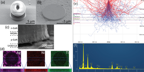
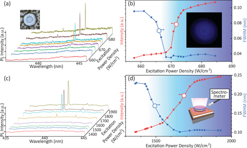
Figure 1c shows a close-up SEM image highlighting the metallic undercut formed after the wet etch using Aqua Regia solution. The SEM image clearly reveals a gap, estimated to be approximately 100 nm, interposing the microdisk and the eutectic bonding layer beneath it. Given the diminutive nature of the air gap and the challenges inherent in confirming its consistent presence around the entire microdisk perimeter, an SEM-Energy Dispersive X-Ray spectroscopy (EDX) has been conducted to verify and identify the pivot formation, as shown in Figure 1d,f. At an accelerating voltage of 20 kV, where the EDX map is obtained, the interaction volume is sufficiently large to penetrate the 500 nm-thick LED thin film and generate X-rays from the eutectic bonding layers. This is corroborated by the Monte Carlo simulation of electron trajectory using CASINO[43] presented in Figure 1e. Interestingly, there are still signals of Ni and Ag from the region outside the microdisk. This suggests that the wet etch is anisotropic, with a higher etch rate in the horizontal direction when the Ni/Ag/Ni/Au layer is deposited atop a GaN layer. This phenomenon may be attributed to the wetting properties of the neighboring layers as suggested in a previous study.[44] Consequently, the etch depth attributable to the wet etching process is estimated at approximately 180 nm–the cumulative thickness of the Ni/Ag/Ni/Au stack. This estimation aligns with the SEM-detected air gap of 100 nm, suggesting that the etching extends more deeply within the microdisk's domain.
It is evident that the X-rays from beneath the LED film are considerably weaker than those generated on the exposed metallic surface outside the microdisk region, resulting in higher signal intensity outside the microdisk. Within the microdisk region, the central portion, approximately 4 in diameter, exhibits a higher EDX signal for Nickel and Silver compared to the circumference region. However, the Ti EDX signal inside the microdisk shows little change. This indicates that the wet etch using the Aqua Regia solution has successfully removed the Ni/Ag/Ni/Au layer in the circumference region while leaving the central part intact for metallic pivot formation. Since Ti features a slower etch rate than Ni in the Aqua Regia solution, it acts as an etch stop during the 3-s wet-etch process.
The lasing characteristics of the fabricated microdisks are investigated using micro-photoluminescence (-PL) measurements. As can be inferred from the -PL spectra in Figure 2a,c, the lasing peaks occur at 446.5 and 439.9 nm for microdisks with and without metallic undercut, respectively. Notably, in the absence of undercutting, the microdisks still achieve lasing, facilitated by a reflective bottom layer that provides optical confinement, boasting a reflectivity in the range of 60%–80%. The plots of linewidth and PL intensity with respect to excitation power density reveal the improved lasing performance of the thin-film microdisk when a metallic undercut is applied. Following the undercutting, the linewidth at the lasing threshold is reduced from 0.134 to 0.036 nm, corresponding to Q factors of 3300 and 12400, respectively. The lasing threshold also exhibit a decrease from.1550 to 670 Wcm−2 after the undercutting. Furthermore, the lasing characteristics of the microdisk with metallic undercut is confirmed through a coherence length measurement using a home-built Micheslon interferoemter. The inset of Figure 2b displays the circular fringe formation, indicative of the laser coherence, with the coherence length measured to be in the vicinity of 0.7 cm.
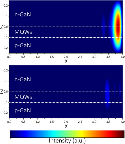
3D finite-difference time-domain (FDTD) simulations using Lumerical FDTD software substantiate that the performance enhancement primarily results from improved optical confinement. This is illustrated in Figure 3, which showcases a higher electric field intensity in the microdisk with metallic undercut. Given that the sole difference between the two simulation cases is the metallic undercut, it can be concluded that undercutting the thin-film microdisk leads to a substantial improvement in optical confinement. This improvement is likely attributed to the enhanced reflection at the GaN/air interface, which contributes to superior waveguiding effect along the microdisk circumference. In contrast, the silver layer deposited at the bottom of the GaN along the microdisk circumference induces absorption, which adversely affects the WGM. With the implementation of metallic undercut, The Q factor of the design is estimated to be improved from 10000 to 56300 with the metallic undercut, as extracted from 3D finite element simulations using COMSOL. Notably, the simulated Q factor experiences a marked increase when the imaginary component of the silver's refractive index is nullified. This observation implies that, despite the undercut, the extended evanescent tail of the WGM resonant field continues to interact with the metallic region, culminating in optical losses.
To further investigate the impact of the metallic pivot formation, scanning near-field optical spectroscopy (SNOS) PL measurements are conducted. Given the relatively low thickness of 500 nm for the thin film sample and the large diameter of the microdisk, the effective spatial resolution of the mapping primarily depends on the equipment's pixel resolution when scanning the area, which is approximately 160 nm. Figure 4 displays the near-field PL maps acquired from the fabricated thin-film microdisk with metallic undercut. The near-field PL intensity map in Figure 4a demonstrates that the highest PL intensity is found in the central region of the microdisk, which also exhibits the longest peak emission wavelength, as illustrated in Figure 4b. The shorter wavelength observed in the circumference region outside the pivoted area implies that strain relaxation resulting from the undercut may have induced a spectral blue-shift. A relative spectral red-shift is detected at the edge of the microdisk, a phenomenon that is elaborated upon in our previous studies.[45]
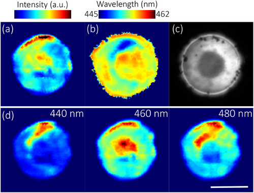
However, the PL map in Figure 4c, obtained using a Carl Zeiss LSM700 laser scanning confocal microscope with a 405 nm continuous wave laser at 100 mW, reveals a different trend: the central region exhibits lower PL intensity than the circumference region. The confocal technique resembles conventional -PL measurement but incorporates a confocal pinhole to enhance spatial and depth resolution. As a result, it can be inferred that the metallic pivot absorbs a portion of the excitation optical power, particularly at the shorter excitation wavelength of 405 nm, where absorption is more pronounced relative to the PL emission wavelength. This leads to a diminished PL response in the central region. In contrast, with SNOS, the fiber tip excites PL at a near-field distance and diverges significantly thereafter, which in turn diminishes the impact of the laser reflection on the resultant PL signal. Although the 405 nm excitation laser employed in SNOS is still subject to absorption by the underlying metal structure, the proximity of excitation and subsequent PL collection near the microdisk's surface minimizes the contribution of both the reflected laser and the excited PL from the metal post within the total near-field PL signal. Taking these factors into account, the SNOS near-field PL results can be analyzed using additional measurements of wavelength-resolved near-field PL maps.
As depicted in Figure 4d, the central region of the microdisk exhibits slightly lower intensity at 440 and 480 nm, while at 460 nm, the central region has higher intensity. This phenomenon can be attributed to the optical confinement effect arising from the thin film's thickness. Wavelengths around 460 nm are not optimally confined when the bottom and top surfaces are considered as a Fabry-Perot cavity. Consequently, the PL, enhanced by the reflectivity of the bottom metallic pivot, leaks out of the microdisk with a higher intensity at the central region. On the other hand, emissions at 440 and 480 nm are readily confined as WGM within the microdisk. This confinement, in conjunction with the strain relaxation effect that causes spectral blue-shift at the circumference region, accounts for the slightly higher intensity observed at the circumference region.
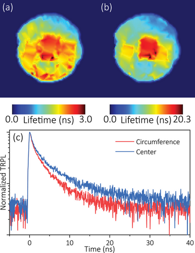
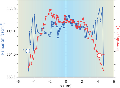
To corroborate the aforementioned interpretation, the microdisk is further examined using a time-correlated single photon counting (TCSPC) setup in conjunction with the SNOS. As illustrated in Figure 5, the central region exhibits longer lifetimes than the circumference region. This observation can be attributed to an increase in electron-hole wavefunction overlap due to a reduction in the Quantum Confined Stark Effect (QCSE) within the MQWs as the strain relaxes[46-48] in the circumference region, aligning with our observations and interpretation from the near-field PL map. Furthermore, the strain relaxation effect resulting from the metallic undercut is characterized by Raman spectroscopy. A 532 nm Cobolt 05-01 continuous-wave diode-pumped laser is utilized to excite the sample in a backscattering configuration. Figure 6 shows the line profile of the (high) peak positions along the microdisk. The peaks in the central region and at the edge of the microdisk are located at approximately 564.8 cm-1, while they shift to around 564.4 cm-1in the circumference region. This shift trend corresponds well with the increasing strain relaxation effect caused by the metallic undercut, as observed earlier in the near-field characterization results. It should be noted that the roll-off of intensity near the microdisk edge is due to the large beam spot size; however, this does not impact the Raman spectra.
Having confirmed the strain relaxation effect in the circumference region, it can be inferred that the higher IQE resulting from the reduction in QCSE due to strain relaxation contributes to an enhanced gain. A temperature-dependent -PL analysis was performed, which revealed an increase in IQE of over 40%, rising from 56% – a value akin to the as-grown wafer's IQE of 63%, as reported in our previous study[33]– to 80% following the implementation of the metallic undercut process. This enhanced gain from increased IQE can effectively compensate for optical losses, thereby potentially elevating the Q factor of the active resonator.[34, 35] Additionally, the spectral blue-shift aids in aligning the gain with the lasing peak position. This improved overlap between the gain spectrum and the lasing peak optimizes the lasing conditions, potentially boosting the Q factor and lowering the lasing threshold. Along with improved optical confinement attributed to the metallic undercut geometry, as well as the high overlap factor owing to the optimized cavity thickness associated with the thin-film configuration, the proposed InGaN MQW-based thin-film microdisk laser is able to achieve a high Q factor of 12400.
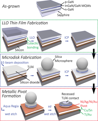
Having characterized and comprehended the benefits of the metallic undercut design, we proceeded to design and fabricate an InGaN-based thin-film microdisk, incorporating a metallic undercut and a top contact, intended for electrical injection. In alignment with the principles underpinning the metallic undercut design, the top contact is subjected to a wet etch process. As a result, the top contact takes the form of a disc situated above the microdisk. Importantly, this disc has a smaller diameter than that of the microdisk, thereby leading to the exposure of the microdisk's circumference. This strategic procedure was executed to circumvent any potential impairment of optical performance that might be induced by the top contact. As the n-GaN layer is highly conductive, the recessed top contact will have a negligible impact on the device's electrical performance.
The optical performance of the microdisk laser under electrical injection is showcased in Figure 7. Current is introduced via a silver nanowire affixed to the microdisk, a method that aligns with our previous investigations. A Siglent SDG6022X pulse generator, functioning at a frequency of 500 kHz and a duty cycle of 15%, serves as the pulsed voltage source to drive the microdisk. The resultant luminescent signal is collected by the PI Acton SP2500 spectrograph coupled with the PIXIS 256E CCD, employing a 2400 gmm-1 grating, akin to the PL setup.
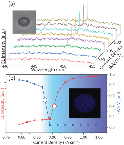
A sharp peak in the EL spectra, as displayed in Figure 7a, along with the clear narrowing of the linewidth, as underscored in the linewidth versus current density plot portrayed in Figure 7b, compellingly indicate lasing. The linewidth of the 449.3 nm lasing peak at the lasing threshold of 0.89 kA/cm2 is 0.044 nm, corresponding to a Q factor of 10100. As per Figure 8 and Table 1, this is the highest Q factor reported to date. It is noteworthy that Ref. [16] reports a similar lasing threshold despite a lower Q-factor, which can be attributed to its smaller microdisk diameter (5.6 ) that results in a reduced active volume, thereby lowering the threshold.[49] The lasing behavior is further substantiated by a coherence length measurement conducted using a Michelson interferometer. The inset in Figure 7b illustrates the circular fringes formed at zero path length difference, and the coherence length is approximated to be about 0.6 cm.
| Year | Threshold (kA/cm2) | Q factor | Linewidth (nm) | Lasing wavelength (nm) | Diameter () | Ref |
|---|---|---|---|---|---|---|
| 2023 | 0.89 | 10100 | 0.044 | 449.3 | 8 | This work |
| 2023 | 5.57 | 2631 | 0.16 | 420.9 | 40 | [20] |
| 2022 | 2.98 | 440 | 1.00 | 440.2 | 100 | [19] |
| 2021 | 0.85 | 3700 | 0.12 | 456.5 | 5.6 | [16] |
| 2020 | 8.00 | 822 | 0.50 | 411 | 20 | [18] |
| 2018 | 12.73 | 1031 | 0.40 | 412.4 | 50 | [15] |
| 2004 | 7.8 | 135 | 3 | 403.5 | 500 | [50] |
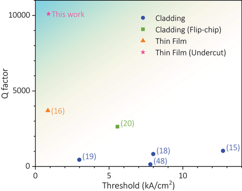
This study marks a significant advancement in the EL lasing performance, particularly in enhancing the Q factor, of InGaN microdisk lasers compared to previous studies. It establishes a promising avenue for the structural optimization of microdisk lasers. Moving forward, we anticipate that continued refinements in this domain will lead to substantial improvements in lasing performance. Specifically, fine-tuning the thickness of the contact stack in conjunction with precise adjustments to the duration of the wet etching process is expected to expand the air gap beneath the undercut, enhancing optical confinement and thereby elevating the Q factor. Furthermore, the application of the metal undercutting technique introduces innovative opportunities for fabricating air-bridged components on thin-film platforms, utilizing wet-etching in conjunction with carefully designed mask patterns. This strategic approach not only improves current laser designs but also sets the stage for future innovations in InGaN based photonic integrated circuit (PIC) technology.
3 Conclusion
This study unveils an innovative approach for enhancing the Q factor of electrically-injected InGaN multi-quantum-well thin-film microdisk lasers via the incorporation of a metallic undercut. This unique combination of a thin-film configuration with the metallic undercut significantly improves both optical confinement and overlap factor. Furthermore, strain relaxation in the undercut region, as characterized by SNOS and micro-Raman line scans, has been identified to substantially mitigate the QCSE. This leads to an increase in the IQE by more than 40%. The emission spectrum exhibits a blue-shift that aligns with the lasing peak, thereby contributing to further enhancement of the Q factor. This methodology results in a high active Q factor of 12400 under room-temperature optical pumping conditions, and an unprecedented active Q factor of 10100 under electrical injection condition, marking the highest recorded to date. The insights derived from this study offer significant contributions to the continuous advancements in microdisk laser technology. The proposed approach holds considerable potential to shape the future of InGaN MQW-based microdisk lasers, thereby laying the groundwork for a multitude of applications in photonics, inclusive of on-chip photonic communications and beyond.
4 Experimental Section
Material
The fabrication process for the microdisk lasers begins with an InGaN LED wafer emitting at a wavelength of 460 nm. This InGaN LED wafer, sourced from Invenlux, was grown on a c-plane patterned sapphire substrate using metalorganic chemical vapor deposition (MOCVD). The wafer structure consisted of an undoped GaN buffer layer and an n-GaN layer, on top of which the MQWs were formed. The MQWs were composed of seven pairs of InGaN/GaN quantum wells, with thicknesses of 4.7 nm and 10.9 nm, respectively. At the top of the wafer structure lies a 150 nm-thick p-GaN layer.
Thin Film Process
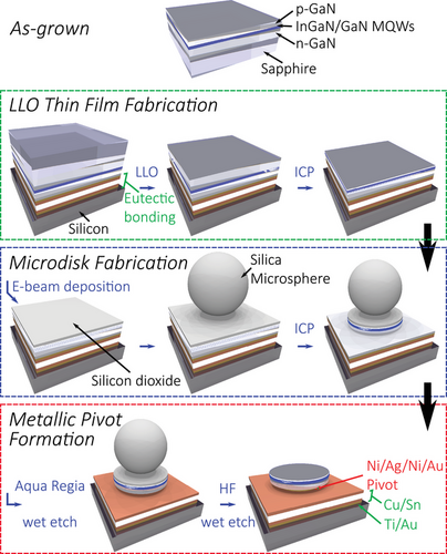
The process flow of the microdisk fabrication was depicted in Figure 9. Initially, a Ni/Ag/Ni/Au (5 nm/100 nm/25 nm/50 nm) reflective metal layer was deposited onto the top p-GaN surface using electron beam deposition. Subsequently, a Ti/Au (30 nm/100 nm) metal layer was deposited on both the LED wafer (on top of the p-GaN metallic layer) and the target Si substrate, followed by electroplating a Cu/Sn bonding layer. By pressing the LED wafer and the Si substrate together, with the Cu/Sn bonding layers in between, under high pressure and temperature, a secure eutectic bond was formed. The sapphire substrate was then removed through a laser lift-off (LLO) process employing a collimated beam from a 266 nm Nd:YAG Continuum Surelite laser. The sample undergoes mechanical polishing to remove the patterned sapphire substrate (PSS) pattern, followed by an ICP etch to eliminate the u-GaN layer and to thin the film to a thickness of approximately 500 nm.
Microdisk Fabrication
The fabrication of the microdisks was carried out on the InGaN LED thin film platform. First, a silicon dioxide layer was deposited using electron beam deposition for pattern transfer. Microsphere lithography, a self-assembled patterning technique, was then employed to create the circular pattern for microdisk fabrication. The thin film sample was initially dispersed with 8--diameter silica microspheres through spin coating. A low concentration of the microsphere solution was used to reduce the likelihood of microspheres clustering together.[22]
InGaN microdisks were formed after transferring the circular pattern to the InGaN LED thin film during the subsequent ICP etch, as shown in Figure 1a. The microdisk sample was then submerged in an Aqua Regia solution for 3 s to undercut the microdisk in the eutectic bonding layer. Since Nickel and Silver rapidly dissolve in the Aqua Regia solution, a metallic pivot was formed with the Ni/Ag/Ni/Au layer deposited directly on the p-GaN layer, leaving the bottom p-GaN surface near the microdisk's circumference exposed to air for optical confinement. Finally, the silica microsphere and the oxide layer were removed by submerging the sample in a hydrofluoric acid solution for one minute.
Micro-Photoluminescence (-PL) Measurements
A CNI pulsed laser, TUN-TiA-393-408, emitting at 393.32 nm with a pulse width of 29.25 ns and a repetition rate of 50 kHz, was utilized for optical pumping of the microdisk. The excited free-space PL signals were collected by an optical fiber bundle placed at an inclination angle of approximately 20. These signals were then coupled to a Princeton Instrument Acton SP2500 spectrograph with a PIXIS 256E front-illuminated charge-coupled device (CCD), offering an effective optical resolution of 0.034 nm using a 2400 gmm-1 grating.
Coherence Length Measurement
Coherence length measurement was conducted by using a home-built Michelson interferometer. The excited lasing signal was first coupled into an Ocean Optics Solarization Resistant Fiber. The beam was subsequently re-emitted into free space and collimated prior to entering the Michelson interferometer. This home-built Michelson interferometer included a beamsplitter and two mirrors, one of which was movable to facilitate the measurement of coherence length. A Nikon camera recorded the circular fringe pattern projected on a white screen, captured at the zero path length mirror position.
Scanning Near-Field Optical Spectroscopy (SNOS)
Scanning near-field optical spectroscopy (SNOS) near-field PL measurements were conducted using an NT-MDT NTEGRA NSOM microscope in an illumination-collection mode. A Coherent CUBE 405 nm continuous-wave diode laser source, operating at 15 mW of power, was coupled to a fiber, with the opposite end serving as an apertured tip to excite PL from the microdisk. The near-field PL signal was then simultaneously collected by the same tip and directed to a Horiba iHR 550 spectrograph with a Syncerity BI UV–vis deep-cooled CCD using a 600 gmm-1 grating.
Time-Resolved Near-Field PL
A 405 nm picosecond pulsed laser source, the Picoquant LDH-405, was coupled to the SNOS fiber tip to excite the sample at a repetition rate of 10 MHz. The collected near-field PL signals were then received by a PicoQuant Hybrid Photomultiplier Detector Assembly (PMA Hybrid). Following this, a PicoHarp 300 TCSPC module measures the time delay by comparing the timing of a received photon with that of the electronic synchronization signal received when the laser pulse was triggered. This time delay data was accumulated to generate a histogram representing the lifetime of the near-field PL. A biexponential decay fitting was performed to determine the lifetimes of the InGaN/GaN MQW multilevel system.[48, 51]
Device Fabrication for Electrical Injection
The process flow for the fabrication is presented in Figure 10. The protocol for preparing the thin film sample via eutectic bonding remains consistent with the one illustrated in Figure 9. However, an additional step was introduced whereby a Ti/Al (5 nm/50 nm) top contact layer was deposited prior to applying the oxide layer for pattern transfer. Following an ICP etch, the Aqua Regia wet etch was carried out, simultaneously shrinking both the metallic eutectic bonding layer and the top contact layer. The device was then passivated by a 50 nm-thick layer deposited by e-beam deposition preceding removal of the microsphere by an HF wet etch step.
Optical Simulations
Optical simulations of the microdisk design were conducted using the software Lumerical FDTD and COMSOL to compute the electric field distribution and estimate the Q factor of the microdisk before and after undercut, respectively. The microdisk was represented by a GaN cylinder with a diameter of 8 and a thickness of 500 nm. In alignment with established studies, the minor absorption effects due to p- and n-type doping were neglected, as doping levels can vary between samples, diminishing the generalizability of the results, and the associated absorption was sufficiently minimal to justify this approximation. A reflective metallic layer, comprising a 100 nm thick silver film, was situated beneath the microdisk, succeeded by a silicon substrate. The simulations incorporate wavelength-dependent refractive index models (both real and imaginary components) for GaN,[52] Ag,[53] and Si,[54] based on values reported in the literature.
In the FDTD simulations, perfectly matched layer boundary conditions are applied to all external boundaries of the simulation domain to minimize reflections. In the COMSOL simulations, scattering boundary conditions were employed on all sides, and an Eigenfrequency study was conducted to extract the Q factors of the microdisks.
Acknowledgements
This work was supported by a General Research Fund (Project 17206922) and an ANR/RGC Joint Research Scheme (Project A_HKU703/17), sponsored by the Research Grant Council of Hong Kong SAR.
Conflict of Interest
The authors declare no conflict of interest.
Open Research
Data Availability Statement
The data that support the findings of this study are available from the corresponding author upon reasonable request.


