Inverted Hysteresis in n–i–p and p–i–n Perovskite Solar Cells
Abstract
A combination of experimental studies and drift-diffusion modeling has been used to investigate the appearance of inverted hysteresis, where the area under the J–V curve for the reverse scan is lower than in the forward scan, in perovskite solar cells. It is found that solar cells in the p–i–n configuration show inverted hysteresis at a sufficiently high scan rate, whereas n–i–p solar cells tend to have normal hysteresis. By examining the influence of the composition of charge transport layers, the perovskite film crystallinity and the preconditioning treatment, the possible causes of the presence of normal and inverted hysteresis are identified. Simulated current–voltage measurements from a coupled electron–hole–ion drift-diffusion model that replicate the experimental hysteresis trends are presented. It is shown that during current–voltage scans, the accumulation and depletion of ionic charge at the interfaces modifies carrier transport within the perovskite layer and alters the injection and recombination of carriers at the interfaces. Additionally, it is shown that the scan rate dependence of the degree of hysteresis has a universal shape, where the crossover scan rate between normal and inverted hysteresis depends on the ion diffusion coefficient and the nature of the transport layers.
1 Introduction
Hybrid metal halide perovskites are mixed ionic–electronic semiconductors with exceptional optoelectronic properties, ideal for applications in photovoltaics,[ 1-3 ] lighting,[ 4 ] lasing,[ 5 ] X-ray detection,[ 6 ] among others. In all these applications, robustness and stability of the material are crucial. Bearing in mind that perovskites are ionic materials, it is expected that ion migration plays a significant role in all stability issues under operational conditions that often are triggered by irreversible ionic displacements.[ 7 ]
The mixed ionic–electronic nature of metal halide perovskites was first described by Eames and co-workers in 2015.[ 8 ] Mobile ion defects have been widely acknowledged to influence charge transport in perovskite solar cells (PSCs) through generation of an electrostatic field profile that partially screens the field due to the applied bias and built-in voltage.[ 9, 10 ] One of the most studied manifestations of ion migration in PSC is current–voltage hysteresis.
Hysteresis is a dynamic effect arising from the slow response of the perovskite material with respect to a change in the external voltage. Experimentally, it has been reported that hysteresis in the current density–voltage (J–V) curve varies with scan rate, scan direction, temperature, crystallinity of the material, and nature of the contacts.[ 11, 12 ] It is well established that ion accumulation at the perovskite/selective contact interfaces causes hysteresis by modifying the internal electric field that drives charge carriers to the selective contacts (electron and hole transport layers).[ 13-20 ] In addition, a second effect related to the alteration of charge carrier injection or extraction at the transport layer interfaces has also been linked to the occurrence of hysteresis.[ 9, 21, 22 ]
Richardson and Courtier et al.[ 13, 15 ] used drift-diffusion (DD) modeling to show that normal hysteresis can be explained by the slow reorganization of the mobile ions at the transport layer interfaces when the external voltage changes. This causes a favorable internal electric field for charge collection in the reverse scan, and an unfavorable internal electric field in the forward scan, hence DoH > 0. Cave et al.[ 19 ] showed that the scan rate at which the DoH reaches a maximum gives a measure of the time taken by the mobile ions responsible for hysteresis to move through the perovskite layer, determined by the diffusion coefficient of the mobile ions D ion.
In contrast, inverted hysteresis has been much less studied. Although it has also been associated with the accumulation of charge at the interfaces and the formation of energy barriers,[ 22-25 ] its origin is not well understood yet.[ 10 ] Experimentally, inverted hysteresis effects have been related to compositional changes in the perovskite[ 22, 25 ] or to chemical treatments of the interfaces.[ 26 ]
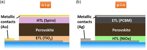
In this article, we report systematic experimental and modeling studies of J–V hysteresis in both p–i–n and n–i–p perovskite solar cells (Figure 1 ). Our experimental results show that inverted hysteresis, like normal hysteresis, is sensitive to 1) the crystallinity of the perovskite layer (affecting ion and charge carrier transport through the perovskite layer), 2) the prebias potential (affecting ion accumulation and depletion near the perovskite layer/charge transport layer interfaces), and 3) the nature of the charge transport layers (affecting charge extraction, injection, and recombination at these interfaces). We show that inverted hysteresis can be seen in both p–i–n and n–i–p cell configurations if a sufficiently large range of scan rates is explored. A simplified description of a PSC, based on a coupled electron–hole–ion DD model, backs up these results, reproducing the crossover from normal to inverted hysteresis well. Analysis of the DD simulation also helps to identify how perovskite and charge transport layer properties affect the shape of the J–V curves.
2 Results and Discussion
2.1 Experimental Results
All our PSCs use MAPbI3 for the perovskite layer. The cell used as our starting point has a planar p–i–n structure, where the hole transport layer (HTL) is spin-coated mesoporous and planar NiO x and the electron transport layer (ETL) is a PCBM ([6,6]-phenyl-C6-butyric acid methyl ester) layer with bathocuproine and a silver contact. This configuration was selected due to its reported low hysteretic behavior.[ 21, 27 ] For comparison, mesoporous n–i–p cells with TiO2 and spiro-OMeTAD as selective contacts were also studied. Details of all devices prepared are collected in Table 1 . Experimental details of the fabrication of the films and devices can be found in the Supporting Information.
| Architecture | Batch | Experimental details | J sc [mA cm−2] | V oc [V] | Efficiency [%] |
|---|---|---|---|---|---|
| p–i–n | 1 | Mesoporous/planar spin-coated NiO x ; fabricated at the University of Bath | 18.1 ± 0.8 | 0.97 ± 0.01 | 12–14 |
| 2 | Spin-coated, planar NiO x only; fabricated at Pablo de Olavide University | 22.3 ± 1.8 | 1.02 ± 0.08 | 14–16 | |
| n–i–p | 1 | Glove box | 19.8 ± 1.3 | 1.01 ± 0.04 | 12–15 |
| 2 | Ambient | 22.8 ± 1.5 | 1.04 ± 0.05 | 14–17 |
Following previous work,[ 21, 28 ] two types of illumination were used (cells were measured at 1 sun under a solar simulator and at 42.5 mW cm−2 using a 465 nm blue LED). Unless otherwise stated all J–V measurements were carried out as follows: under the solar simulator a prebias of 1.2 V was applied for 5 s to maximise the attainable photocurrent, followed by a linear potential scan from 1.2 to 0 V and from 0 to 1.2 V with a step size of 10 mV. At 1 sun, J–V measurements were recorded at 100 mV s−1. Under blue LED illumination, a prebias of 1.2 V was applied for 20 s, followed by a linear potential scan from 1.2 to 0 V and from 0 to 1.2 V with a step size of 10 mV. The scan rate was varied between 1 and 1000 mV s−1. The range of scan rates used was tailored depending on the stability of the individual device being measured and the reliability of the results obtained at the fastest scan rates, evaluated by the shape of the J–V scans. Longer prebias times were not investigated to prevent cell degradation.
Devices were prepared in two different laboratories (University of Bath for batch #1 and Pablo de Olavide University for batch #2) and with two different methodologies to ensure the universality of the results. Efficiencies obtained under 1 sun illumination for the devices studied in this work lie around 12–14% for batch 1 and 14–16% for batch 2 (J sc = 22.3 ± 1.8 mA cm−2, V oc = 1.02 ± 0.08 V), in line with average values reported in the literature for p–i–n MAPbI3-based solar cells with undoped NiO x layer as the HTL and PCBM as the ETL.[ 29-31 ] It is worthy to mention that, although higher efficiencies have been reported for inverted perovskite solar cells with similar components to the ones presented in this work,[ 30-35 ] they usually require doping of the selective layers or to modify the perovskite layer to improve the efficiency. Here, we focused our effort on the study of the hysteretic behavior of inverted perovskite devices without modification of the selective layers. More details about the characterization protocols and photovoltaic data are collected in the Supporting Information (Figure S2, S3, S5, S8, S9, Supporting Information).
The scan rate variation of the DoH was measured under blue illumination. Figure 2 shows results for cells of batch 2. Results for batch 1, where three different types of NiO x layers are compared, are presented in Figure S4 and S5, Supporting Information. For both batches we see that the DoH changes sign for p–i–n cells at scan rates exceeding 5 mV s−1. In contrast, in the most common configuration of a mesoporous n–i–p cell the DoH is positive, being only negative at scan rates greater than 1000 mV s−1 in some devices of batch 1 (Figure S4, Supporting Information), i.e., for cells prepared inside a glove box. Extreme care was taken with high scan rate measurements to ensure that it was still possible to obtain sensible measurements under these conditions.[ 26 ] To confirm this we measured one device from slow to faster scan rates, reproducing the same behavior (crosses in Figure 2 left).
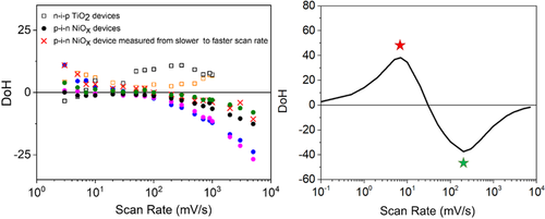
Our results in Figure 2 and S4, Supporting Information, evidence that the nature of the contacts (e.g., TiO2 and Spiro or NiO x and PCBM) influences the hysteresis more than whether the layer is nanostructured or not, or if the NiO x layer is spin-coated or sprayed on the substrate. Comparison of results from batch 1 and batch 2 indicates that more efficient devices have, in general, less hysteresis than less efficient ones. It should also be noted that the perovskite film may crystallize differently on a TiO2 film compared to on a NiO x film, as well as in different environments (glove box vs ambient) or depending on the posttreatment (vide infra), which could account for the different responses measured. In the following, we analyze the sensitivity of hysteresis to the crystallinity of the perovskite.
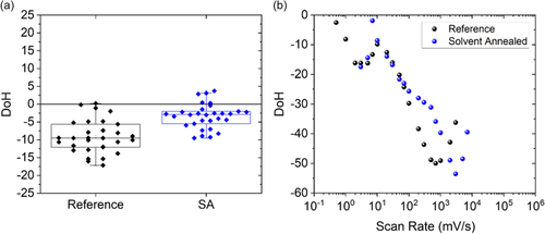
We have used solvent annealing to evaluate the influence of the crystallinity on inverted hysteresis (see Figure S1, Supporting Information, and details of the preparation procedures in the Supporting Information for cells in batch 1 and Figure S2, Supporting Information, for the photovoltaic data). The normalised X-ray diffraction (XRD) spectra for a standard perovskite film and a solvent annealed film are reported in Figure S6 and S7, Supporting Information. These data show the characteristic tetragonal peak at 14.2º (110).[ 28 ] but the solvent annealed samples do not have the characteristic (004) peak at 28.11° and do have a sharper peak at 28.36° (220). There is a clear difference in the intensity of the diffraction peaks in a non-normalized diffraction plot. This observation is a strong indication of higher crystallinity of the sample with solvent annealing and has been reported for other samples treated in this way.[ 36, 37 ] The impact of crystallinity on the hysteresis can be observed in Figure S8, Supporting Information (J–V curves of three devices with and without solvent annealing treatment) and Figure 3 (DoH). Most of the solvent annealed cells showed inverted hysteresis, although a few showed normal hysteresis at 100 mV s−1. We observed that the DoH is considerably lower for solvent annealed PSCs than for regular devices at 100 mV s−1, shifting the DoH min toward faster scan rates. Interestingly, the hysteresis is much higher under illumination from a blue LED than from sunlight.
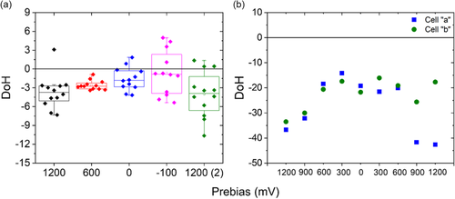
We have also investigated the influence of preconditioning on the occurrence of inverted hysteresis in the solvent-annealed cells. Results for batch 1 can be found in Figure S9, Supporting Information (J–V curves) and Figure 4 (DoH). We found out that the hysteresis depends on the prebias potential and comparing DoH values from prebias of 1200 mV (black and green diamonds in Figure 4a) suggests that these changes are somewhat reversible (although it is clear that some devices were indeed changing due to stress produced by the preconditioning and the solar illumination). Better reproducibility is obtained when the characterization is performed under blue light illumination (Figure 4b), where the reversibility effect is more clearly seen. In any case, although the DoH is strongly dependent on the preconditioning potential, inverted hysteresis is detected in all cases.
To summarize all of the experimental observations: 1) regardless of the configuration and the batch studied, hysteresis was present in all devices and the value of DoH depends on the scan rate as previously reported;[ 19 ] 2) both p–i–n and n–i–p perovskite solar cells can show inverted hysteresis for sufficiently high scan rates; 3) as has previously been reported for normal hysteresis, inverted hysteresis is also sensitive to the nature of the contacts, the crystallinity of the perovskite layer, and the prebias applied to the PSC before the J–V measurement.
2.2 Modeling and Discussion
In order to get some rationale of the hysteretic behavior reported in the previous section we apply DD modeling. Specifically, we use a DD approach (implemented in the IonMonger code[ 38 ]) that includes transport and recombination of charge carriers (electrons and holes) in the active layer (perovskite), transport of a single positive ionic species (iodine vacancies in the perovskite), and electron and hole transport in the electron transport layer and hole transport layer, respectively. The charge carriers and ions are fully coupled through including the electron and hole charge densities with the ion charge density in the Poisson's equation. This model has been extensively validated for n–i–p devices.[ 13, 15, 19, 20, 39 ]
Simulated J–V curves at different scan rates for the case studied in Figure 2b are collected in Figure S10, Supporting Information. For simplicity, we have restricted the hysteresis analysis to a situation where recombination is assumed to take place only in the bulk of the perovskite layer. However, extending the simulations to other scenarios (surface recombination and mixed surface/bulk recombination) leads to the same predictions for the hysteresis scan rate dependence, as shown in Figure S11, Supporting Information. More numerical details can be found in the Supporting Information. Parameter values used are collected in Table S1, Supporting Information.
The key features of the model, which give rise to hysteresis, is that ions move much more slowly than the electron/holes and that they have a concentration which is high enough to effectively screen the external potential (built-in plus applied potential) at sufficiently long times, but only partially at shorter times. The consequence of this screening effect is the formation of space charge layers (also known as Debye layers) in the vicinity of the ETL and HTL and the dynamic alteration of the internal electrical potential depending on the scan rate, scan direction, and the preconditioning history of the device (see Figure 5 ).
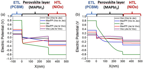
Figure 2 right panel shows the prediction of the DD model for the scan rate dependence of the DoH in the p–i–n cell. Figure S11, Supporting Information, is the same hysteresis index plot with alternative choices for the recombination mechanism. In general, we observe that the modeling can replicate the crossover from normal to inverted hysteresis observed in the experiments as we move from lower to higher scan rates. Interestingly enough, this behavior is maintained, even in the scenario where nonradiative recombination is suppressed. As proof of internal self-consistency, we verify that at sufficiently low or high scan rates (not necessarily reachable in the experiments) no hysteresis is predicted. This is explained by the fact that if the scan is slow enough, ions do have time to reorganize themselves in the Debye layers at all times. If the scan is fast enough, ions get “frozen” in the initial distribution at all times. In either case the electric potential at a given bias is the same, regardless of the scan direction, and no hysteresis is observed.[ 19 ] Clearly, the actual scan rates, where maximum hysteresis is found (either normal or inverted), would depend on the ionic diffusion coefficient[ 19 ] or the transport layer properties.[ 15 ] Here, we pick the two scan rates marked with red and green stars in Figure 2 right panel, which corresponds to maximum normal and inverted hysteresis, respectively, to develop our discussion.
The left panel of Figure 5 shows potential profile snapshots at DoH max where normal hysteresis is seen. From the potential profile where the applied voltage (V app) equals the voltage at the maximum power point (V mpp) during the reverse scan, it can be seen that in the perovskite films the potential has a negative slope driving electrons toward the ETL and holes toward the HTL, increasing J. In contrast, the potential profile at V mpp during the forward scan has a positive slope driving the charges in the “wrong” direction. These changes of slope between the reverse and the forward scan are originated by the reorganization of the ions at the interfaces (see Figure S12, Supporting Information), which is the reason why DoH depends on the scan rate and the ion diffusion coefficients as shown below.
This mechanism explains why there is more hysteresis with monochromatic blue light in comparison with sunlight in the less efficient cells. Hysteresis arises from the interplay between recombination (which determines charge collection at the transport layers) and the acting electric field (which depends on scan rate, direction, and preconditioning). The optical penetration depth for blue light in MAPbI3 is about 200 nm.[ 40 ] The perovskite film in our cells is ≈300 nm thick, implying that the blue light will be absorbed closer to the NiO x contact. The diffusion length L = √(Dτ) is 200–300 nm for electrons and >>300 nm for holes using the parameter values in Table S1, Supporting Information. A strong impact on the collection is then expected if electrons are photogenerated far from the ETL. Hence, changes in the acting electric field caused by ionic reorganization would give rise to more hysteresis with blue light than with white light, where carriers are more homogeneously photogenerated.
The right panel of Figure 5 shows potential profile snapshots at DoH min. In the case of inverted hysteresis, the slopes of the potential profile snapshots when reaching V mpp during forward and reverse scans are also different, but the change of slope is less pronounced and appears to be restricted to the vicinity of the ETL only whereas in the rest of the active layer the electric profiles tend to be flat. This observation is connected with the fact that the ionic distributions do not change much with scan direction in this case because inverted hysteresis only appears at high scan rates and ions do not have time to adapt to voltage changes (right panels in Figure S8, Supporting Information). This also helps to explain the experimental result of why the V oc changes more dramatically between scan directions at higher scan rates (Figure S9, Supporting Information). Hence, inverted hysteresis is always associated with a less intense alteration of the ion distribution with the scan direction due to a fast change of the applied voltage.
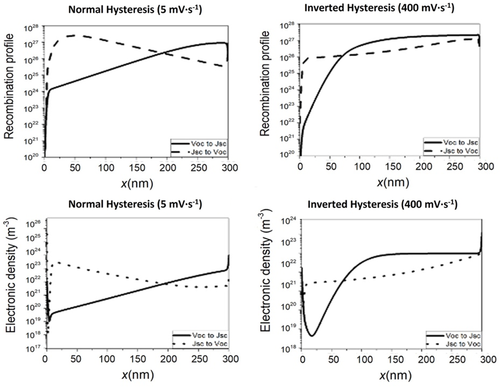
To cast more light on the origin of the different behavior observed for normal and inverted hysteresis, we show in Figure 6 the recombination and electronic density profiles (sum of the electron and hole concentrations) at the maximum power point at two scan directions. As the model calculates the recombination rates from the local electronic density (using the Shockley–Read–Hall [SRH] model, the recombination rate is proportional to the density of electronic carriers, see Section 2, Supporting Information), the recombination profiles reflect the electronic density profiles. Bearing this in mind, in the case of normal hysteresis, both the electronic density and the recombination profiles reflect the same change of slope between the forward and the reverse scan that is observed in the electrical potential (Figure 5 left panel). As we said above, this change of slope is what favors collection in the reverse scan with respect to forward scan producing the normal hysteresis pattern. In contrast, for inverted hysteresis, the recombination rate and the electronic density profiles change dramatically between forward and reverse scan but only in the vicinity of the ETL interface. This explains why changing the contacts (Figure 2) modifies the onset of the transition from the normal to the inverted regime. As a matter of fact, as it can be observed by comparing both panels in Figure 5, the electric potential values for both scan directions at the ETL when there is inverted hysteresis (right panel) are swapped at the maximum power point (where the difference between scan directions is largest) with respect to the normal hysteresis case (left panel). This means that there is an additional energy barrier for electron injection in the reverse scan with respect to the forward scan which leads to lower current in the reverse scan, hence producing inverted hysteresis.
In Figure 7 we show that, according to the model, the mobile-ion diffusion coefficient determines the scan rates for maximum normal and inverted hysteresis. Our results show that an increase in D ion or in N ion causes the scan rates for DoH max and DoH min to increase. In fact, we can say that the DoH scan rate plot can be represented by an S-shaped universal curve, whose position in the time scale depends on the speed and ability of the ions to respond to external voltage changes (which, in turn, depend on the active layer and transport layer properties).
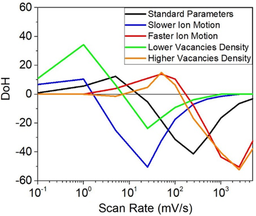
Figure 7 helps to explain the experimental results of Figure 3 and the distinct behavior observed when cells from different batches are compared. It is unlikely that solvent annealing would increase N ion so the modeling predictions lead to the conclusion that solvent annealing increases D ion. As mentioned, solvent annealing leads to higher crystallinity.[ 36 ] Hence, the increase of the ionic mobility in the solvent annealed sample can be understood as a consequence of having fewer grain boundaries. This conclusion is consistent with ions moving faster in the grain bulk than along grain boundaries as shown by atomistic simulations and experimental observations that show that defects are trapped at the grain boundaries,[ 41 ] thus inhibiting their diffusion.
3 Conclusion
Measurements of the scan rate dependence of the DoH for n–i–p and p–i–n hybrid perovskite solar cells prepared using several different experimental procedures (planar or mesoporous oxides, solvent annealing) reveal a universal curve, in which the hysteresis switches from normal to inverted when the scan rate is sufficiently increased. A fully coupled electron–ion DD model replicates this behavior and demonstrates that the actual scan rates for which maximum normal or inverted hysteresis is observed, as well as the crossover scan rate between the two regimes, depend on the ion diffusion coefficient, the ion concentration, and the nature of the electron and hole transport layers. The model also shows that inverted hysteresis is always associated with a less intense variation of the ionic distribution at the interfaces due to a fast change of the applied voltage (i.e., the scan rate). These results provide unique insight into the mechanisms of charge transport in these hybrid perovskite materials, which may prove essential for the design and development of stable perovskite solar cells.
Acknowledgements
R.G.-R. and A.J.R. contributed equally to this work. The research was funded by the European Union's Horizon 2020 research and innovation program under the EoCoE II project (824158). J.A.A., G.O., and A.R. thank Ministerio de Ciencia e Innovación of Spain, Agencia Estatal de Investigación (AEI) REFERENCIA DEL PROYECTO/AEI/10.13039/501100011033, and EU (ERDF) under grants PID2019-110430GB-C22 and PCI2019-111839-2 (SCALEUP) and Junta de Andalucía for support under grant SOLARFORCE (UPO-1259175). The work was also supported by the Royal Society (UK) under grant number ICA-R1-191321, AMEXCID SRE-CONACYT (Mexico) grant number 2016-1-278320, and CONACYT FORDECYT-PRONACES (Mexico) projects 848260 and 318703. The authors gratefully acknowledge support from the Ministerio de Universidades and Universidad Pablo de Olavide (Spain) through the Beatriz Galindo program under project BEAGAL 18/00077 and grant BGP 18/00060. A.R. thanks the Spanish Ministry of Education, Culture and Sports via a Ph.D. grant (FPU2017-03684). L.J.B. was supported by an EPSRC funded studentship from the CDT in New and Sustainable Photovoltaics, reference EP/L01551X/1. R.G.R. gratefully acknowledges CONACYT for support through a postdoctoral scholarship. K.V.V. acknowledges CONACYT for support through “Beca de movilidad 2018.” M.V.C. was supported by the EPSRC Centre for Doctoral Training in Sustainable Chemical Technologies EP/L016354/1.
Funding for open access publishing: Universidad Pablo de Olavide/CBUA.
Conflict of Interest
The authors declare no conflict of interest.
Open Research
Data Availability Statement
The data that support the findings of this study are available from the corresponding author upon reasonable request.


