An Efficient Multi-Core DSP Power Management Controller
ABSTRACT
Today's society has entered a digital era, and the use of DSP is becoming increasingly frequent and important. In order to achieve the market targets of high energy efficiency, it is necessary to integrate low-power design from the chip design stage. Based on FT-xDSP chip architecture, this work designs a power management controller for DSP suitable for multi-core and multi-integrated peripherals from the perspective of power control in the chip design stage. This controller can precisely control the power supply, clock, and memory of each module in the DSP and introduces a clamp control unit in the power management controller to solve the problem of possible glitches during asynchronous reset and ensures that the system has no overflow of redundant requests. Additionally, a configurable state transition counter is also set up to avoid the problem of insufficient state transition time for low-speed peripherals or long waiting time for high-speed peripherals. After the pre-tapeout experiment and post-tapeout testing data analysis, the above new power control manager has excellent power management performance. In the low power consumption state of the chip, the overall power consumption of the core is reduced by over 95%, which is of great significance for achieving high-efficiency processor chips.
1 Introduction
Digitization is a mainstream aspect of modern society. With the continuous advancement and innovation of technology, Digital Signal Processor (DSP) is becoming increasingly close to people's production and life and occupies an important position in practical application. It has been widely used in fields such as multimedia, automatic control, and seabed exploration due to its powerful computing power and high-precision real-time processing capability [1].
Digital Signal Processors (DSPs) have a significant impact on modern computing due to their high-speed processing capabilities and real-time data analysis. Their applications extend to various domains such as multimedia processing, telecommunications, medical imaging, and autonomous systems. For instance, in multimedia applications, DSPs are used for video compression, audio enrichment, and real-time speech recognition [2]. In the medical field, DSPs permit efficient MRI and CT image reconstruction. They improve diagnostic accuracy [3]. The telecommunications industry makes use of DSPs for modern signal modulation in 5G networks. This ensures faster and more reliable communication. Besides, DSPs are useful for radar signal processing in defense and automotive LiDAR systems. They improve navigation and object detection capabilities [4].
Modern trends designate a growing demand for energy-efficient DSPs in Internet of Things (IoT) devices. Here, low-power operation is essential for extended battery life. Edge AI processing depends on DSPs to implement machine learning algorithms locally. It is an emerging area that reduces the need for cloud dependency. Additionally, developments in deep learning-based DSP optimization lead to improved performance in smart surveillance and robotics [5-9].
DSP, as a core component of modern electronic technology, is gradually improved in processing capability [10] and integrates more and more peripherals, such as SoC (System on Chip) and other system-integrated chips [11]. At the same time, in order to meet the market demand, the current high-performance processors often adopt a multi-processor parallel architecture, which has strong computing power and data bus interaction ability [12]. However, as the integration level, clock frequency, and computing speed of the chip have all reached a new height [13], its power consumption also increases significantly.
Ranjbar et al. [14] did a comprehensive overview of the power management challenges in multicore systems and emphasized the significance of managing power dissipation as multicore architectures become more prevalent. They studied the phenomenon of “dark silicon.” Here, the significant portions of a chip must be powered down to prevent thermal issues. Their work also explored the state-of-the-art methods in power management across different scales of multicore systems. Sai [15] introduced a self-aware power management scheme to address the dynamic and unpredictable nature of multicore microprocessor workloads. This approach is designed to handle unexpected scenarios such as performance degradation, manufacturing defects, and variations in power and thermal impacts over time. Zhan et al. [16] proposed a heterogeneous voltage regulation (HVR) architecture that uses a multi-stage voltage regulation process and integrates onboard and on-chip voltage regulators to optimize power efficiency. The highlight of this approach is that it uses machine learning to predict workload distributions and adapt the HVR system in real time.
Jia and Zhang [17] refined the dynamic voltage and frequency scaling (DVFS) strategies for CPU power management. Conventional DVFS approaches are limited by the granularity of voltage regulators, which restricts their effectiveness during certain workloads. They improved energy efficiency by introducing a more fine-grained dynamic frequency divider into the DVFS system without compromising performance. Zou et al. [18] presented a learning-based power management framework that combines a global power allocator, reinforcement learning, and swift controllers to manage power at multiple levels. This approach enables μs-level power management that significantly outperforms existing DVFS-based strategies. Guerrero-Rodríguez et al. [19] explored the application of power management in electrical systems, specifically in the design and validation of Shunt Active Power Filters (SAPF) using Controller Hardware-In-the-Loop (CHIL) simulations. Their approach reduces Total Harmonic Distortion (THD) in various load types.
Schierloh et al. [20] focused on the optimization of Heating, Ventilation, and Air Conditioning (HVAC) systems through real-time predictive management. Their heuristic optimization approach not only enhances thermal comfort but also significantly reduces electrical costs. Prasad et al. [21] investigated power management strategies for hybrid AC/DC microgrids by utilizing an Adaptive Neuro-Fuzzy Inference System (ANFIS) and Proportional Integral Derivative (PID) controllers to optimize power distribution. Their work emphasizes the importance of autonomous control strategies in managing the complexities of hybrid microgrids. Mohamed et al. [22] explored the role of electric vehicles (EVs) in power management, particularly in grid frequency regulation. The study also demonstrated the potential of EVs to contribute to grid stability by comparing different control strategies for optimizing EV charging and discharging rates. Yifei et al. [23] studied hybrid propulsion systems (HPSs) by addressing the operational management challenges in vehicular systems. They proposed a two-layer hierarchical optimization framework that uses ANFIS and adaptive low-pass filtering strategies and achieves significant reductions in fuel consumption and system loss.
The high-power consumption of the chip consumes a large amount of electrical energy, leading to the chip overheating, device stability decline, poor endurance, and in severe cases, chip damage [24]. Therefore, low-power design plays an extremely important role in the design of high-performance chips. Adding a special power management control unit to DSP is an efficient low-power design method. That is, in the coding phase, different types of DSP integrated modules are controlled using different methods on the basis of their power consumption level so as to achieve low power consumption and high energy efficiency of DSP. However, most of the proposed previously power managers lack comprehensive clock power control [25-27], and no configurable cycle counter was used during the state transition process. In addition, each power manager did not take into account the possibility of glitches caused by asynchronous reset in large-scale designs. The summary of the existing works was presented in Table 1. The aim of this work is to address the problems mentioned above and make improvements, and eventually achieve a relatively ideal power consumption control effect.
| Reference | Technique | Application area | Advantages | Limitations |
|---|---|---|---|---|
| Ranjbar et al. [14] | Dynamic voltage and frequency scaling (DVFS), power gating, thermal management | Multicore systems | Provided an overview of power management techniques; addresses power dissipation causes and effects | Presented a survey; lacks in implementation |
| Sai [15] | Self-aware power management using machine learning | Multi-core microprocessors | Dynamically adjusts power settings based on workload; predicts future workloads for optimization | Faces computational overhead from continuous monitoring and prediction |
| Zhan et al. [16] | Heterogeneous Voltage Regulation (HVR) with Machine Learning Adaptation | Multi-core Processors | Optimizes voltage levels dynamically; improves energy efficiency | High computational cost for machine learning adaptation |
| Jia and Zhang [17] | Fine-grained dynamic frequency scaling (DFVS) | CPU power management | Enhances CPU energy efficiency without degrading performance | Limited to CPU and not generalizable to all DSP architectures |
| Zou et al. [18] | Reinforcement learning for power allocation | Multi-core processors | Fast and autonomous power control; adapts to changing workloads | Complex implementation; requires extensive training data |
| Guerrero-Rodríguez et al. [19] | Controller hardware-in-the-loop (CHIL) simulations | Electrical systems (SAPF design) | Reduces total harmonic distortion (THD); validates controller performance in real-time | Primarily focused on electrical networks, not DSP systems |
| Schierloh et al. [20] | Predictive power management | HVAC systems | Cost-effective power management for buildings; anticipates energy demands | Not applicable to real-time embedded systems; depends on accurate predictions |
| Narasimha Prasad et al. [21] | Adaptive neuro-fuzzy inference system (ANFIS) | Hybrid AC/DC microgrids | Optimizes power distribution autonomously; handles nonlinearities | Requires complex hybrid system modeling; computationally intensive |
| Cai and Matsuhashi [22] | Model predictive control (MPC) | Electric vehicle frequency regulation | Stabilizes grid frequency using EVs; manages energy storage effectively | Dependent on external factors like vehicle availability; requires accurate models |
| Yifei et al. [23] | Two-layer hierarchical power optimization | Hybrid propulsion systems | Significant reductions in fuel consumption; balances power sources | Designed specifically for vehicular applications; limited generalizability |
| Liu et al. [24] | Static reactive power compensator for fault management | Power distribution networks | Enhances grid stability; manages reactive power effectively | Limited application outside electrical grids; failed to address active power issues |
| Lezcano and Da Costa [25] | O/S level interrupt prediction | Android-based power management | Reduces unnecessary wake-ups; improves battery life | Only applicable to mobile platforms; depends on accurate interrupt prediction |
| Altman et al. [26] | Machine learning for FPGA-based power management | Biomedical systems | Enhances energy-efficient computing in FPGA applications; adapts to workload changes | High dependency on ML model accuracy; needs significant training data |
| Shi et al. [27] | Power supply sleep controller | M-DSP architectures | Reduces idle power consumption; manages power states effectively | Lacks adaptability to newer DSP designs; Not able to handle dynamic workloads well |
The progress and novelty in Digital Signal Processor (DSP) technology have made DSPs integral components in various high-performance computing applications. Despite their powerful computational capabilities, DSPs are increasingly confronted by the need for efficient power management due to the significant power consumption associated with high-speed processing and extensive peripheral integration. This research work introduces a novel power management controller designed for the FT-xDSP architecture, which is distinguished by its multi-core parallel control and integration of both high-speed and low-speed peripherals. Unlike existing power management solutions, this controller uniquely addresses three critical issues in DSP power management: comprehensive clock and power control, evasion of malfunctions during asynchronous reset, and adaptable state transition control.
The novelty of this work is the introduction of a clamp request control unit, which ensures the stability of the system by preventing redundant requests during asynchronous resets, a problem often overlooked in former designs. Additionally, the configurable state transition counter is a novel feature that allows for the precise adjustment of clock switching processes based on the specific needs of different peripherals, thereby optimizing power efficiency without compromising system performance. Existing works typically focus on either clock gating or power gating independently. But the proposed approach integrates both techniques with a flexible control mechanism that adapts to the dynamic power needs of the DSP. This integration results in a significant reduction in power consumption—by approximately 95.9% in clock-gated states and an additional 41.4% when power gating is applied—thereby pushing the limits of energy efficiency in DSP design.
- This work introduces a novel power management controller designed specifically for multi-core DSPs, such as the FT-xDSP architecture. The controller is able to manage power supply, clock, and memory operations for both core and high-speed peripherals and ensures efficient power utilization across different operational states.
- To address the issue of glitches during asynchronous resets, this work introduces a clamp request control unit. This unit effectively clamps low-power components to an invalid state before entering a reset state, preventing redundant requests and ensuring system stability.
- The controller includes a novel feature called a configurable state transition counter that allows for the precise control of state transitions, particularly for low-speed and high-speed peripherals. This counter ensures that transitions occur without timing conflicts and optimizes power management across varying operational conditions.
The remaining sections of the article are structured as follows: Section 2 presents an outline of FT-xDSP Architecture. Furthermore, this section describes the methods used to analyze the power consumption of different components within the FT-xDSP. Section 3 elucidates the structure of the power management controller. Section 4 elaborates on the workflow of power consumption control. Experiments in terms of functional verification and power consumption analysis are presented in Section 5. Section 5 concludes the research work with future directions.
2 Materials and Methods
2.1 A Low-Power Consumption Design Overview
2.1.1 An Overview of the FT-XDSP
FT-xDSP is a multi-core digital signal processor designed for high-performance computing by focusing on energy efficiency. The architecture consists of the following key components:
Multi-Core Parallel Processing: FT-xDSP utilizes a parallel processing architecture with multiple DSP cores to handle complex computational tasks efficiently. Every core consists of independent instruction controllers, arithmetic logic units (ALUs), and caches. This facilitates the concurrent execution of multiple processes.
Heterogeneous Peripheral Integration: The architecture integrates both high-speed and low-speed peripherals to support various applications. High-speed peripherals comprise PCIe, SRIO, and high-speed storage interfaces. It ensures efficient data transmission. Low-speed peripherals, such as I2C and GPIO, enable communication with external devices.
Dynamic Power Management: FT-xDSP has a configurable power management controller that optimizes energy usage by dynamically adjusting clock speeds. It enables or disables power domains and implements both clock gating and power-gating techniques.
Advanced Memory Management: The system includes dedicated memory banks and a storage management component (SMC) that efficiently handles data storage and retrieval. Cache memory is optimized to reduce power consumption and also to maintain high processing speeds.
FT-xDSP adopts multi-core parallel control, and the core part mainly includes the instruction controller, arithmetic logic unit, and caches, implementing the functions of instruction fetch, decoding, instruction flow control, scalar and vector operation, and interrupt exception. Meanwhile, the periphery of the core integrates a large number of peripherals, divided into low-speed peripherals and high-speed peripherals, mainly including I2C, GPIO, SRIO, PCIE, and so on. Among them, the low-speed peripherals mainly interact with the core through the configuration network, including the keyboard, mouse, and so on. High-speed peripherals mainly interact with the core through the data network, including high-speed storage peripherals, network cards, and so on. In addition to the aforementioned cores and integrated peripherals, the memory banks (e.g., memory, SMC [storage management component]) undertake the storage function of the chip. The main structural framework of the FT-xDSP digital signal processor designed in this work is shown in Figure 1.
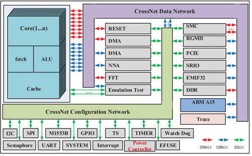
Given the complex structure, diverse functions, and significant power consumption differences of various functional components in FT-xDSP chips, achieving high energy efficiency of the chip requires a powerful but precisely controllable power management controller. With the help of this controller, precise control of the on and off states of each component during chip operation will be achieved based on its real-time working status, minimizing power consumption without affecting performance.
2.2 Power Consumption Analysis of the Ft-XDSP
Power consumption analysis is extremely important for chips, as the power consumption control chip can improve the user experience and realize the system integration optimization. Power consumption mainly comes from two aspects: dynamic power consumption and static power consumption [28-30]. During the operation of a peripheral, dynamic power consumption mainly refers to the power consumption generated by the changes in circuit activity (e.g., charge transfer occurs in transistors during logic state switching) [31]. For the units with high operating frequencies and frequent signal changes, dynamic power consumption is relatively high.
Static power consumption refers to the power consumption of a circuit in a steady state when there is no state transition or signal flip. Generally, every component in the chip has a static power consumption [32]. From the structure of FT-xDSP (Figure 1), it can be analyzed that each integrated peripheral (including low-speed peripheral and high-speed peripheral) and core in the chip has dynamic power consumption. However, in terms of power consumption, low-speed peripherals often have low transmission rates and intermittent operation modes, so their power consumption is relatively low [33].
The high-speed peripherals can interact with the devices connected to the chip in real time and undertake the task of high-speed transmission and storage of data. The cores need to perform parallel processing and instruction dispatch of large amounts of data during operation, while the memory banks are used to store binary data in the chip and flip frequently. Therefore, high-speed peripherals, cores, and storage banks are very power-consuming [34]. For FT-xDSP, the power consumption analysis is shown in Figure 2.
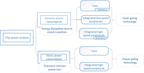
There are many methods to reduce static power consumption and dynamic power consumption, which are generally divided into manufacturing technology and non-manufacturing technology. The manufacturing technology methods include the use of low-power consumption peripherals, optimizing the transistor structures, and so on, while the non-manufacturing technology methods include system-level optimization code control technology.
The work mainly classifies, manages, and controls the peripherals based on their power consumption types to achieve the goal of low-power consumption design. Eliminating dynamic power consumption is mainly realized through clock gating technology [35] in non-manufacturing technology means. This technology uses a power management controller to send clock switch control signals to the clock control component, thereby controlling the clock gating of the corresponding module [36]. The operating frequency of low-speed peripherals in chips is relatively low, and the circuit design is simple, resulting in much lower static power consumption compared to the core and high-speed peripherals. Therefore, the power consumption controller designed in this work only controls its clock, not its power. With the gradual improvement of manufacturing technology, the static power consumption of cores and high-speed peripherals with high clock frequency and complex functions is also increasing. Therefore, it is not enough to reduce their dynamic power consumption solely through clock gating technology. The power management controller designed in this work also adopts power gating technology [37] to reduce its static power consumption. The process of power gating technology employs the Unified Power Format (UPF) technology, which defines the power domain and controls the turning off and on of the power domain through the control signals issued by power management control [38-40].
In addition, as the demand for cache capacity increases, the proportion of power consumption generated by cache in the core and high-speed peripherals also increases. The method to reduce cache power consumption is mainly to control the functional signals of the memory bank to select between power-off or sleep mode. Cache power-off requires the storage model to meet the attribute of power off, and then it can be directly controlled through chip selection and power signal control. The power management controller designed in this work can turn off the clock or power supply of the core and high-speed peripherals while also turning off their cache power to further reduce power consumption during power control.
2.3 Main Structure of the Power Management Controller
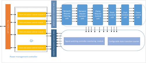
The main structure of the power management controller is shown in Figure 3, which includes a bus interface module, a clock power control module, a state transition control module, and a state transition monitoring module. The bus interface module is mounted on the configuration network, and based on the power management request sent by the core; it enables the power management process of a certain “clock (or) power control module n”. The implementation of power management is accomplished through the simultaneous operation of the state transition control module and the state transition monitoring module.
2.3.1 State Transition Control Module
The state transition control module is responsible for completing the clock/power switching and sending out corresponding control signals. This module includes a network request clearing unit, a network request isolation unit, a clamp request control unit, a reset control unit, a clock control unit, and a power supply control unit.
When applying a power manager, not all peripherals are used simultaneously, and it is generally determined according to the needs of users. The components that do not need to work currently will be controlled by low-power consumption technology. When the ecosystem of a chip is working in an orderly manner, controlling arbitrarily a component into a low-power state may cause the entire chip to work disorderly or even crash. Therefore, before implementing low-power technology control on a component, the network request clearing units and network request isolation units are used [9], as the other power consumption controllers do, to ensure the normal operation of the system.
Furthermore, the low-power management of the chip is generally carried out in the reset state, which can greatly avoid conflicts between access and requests. When performing a system reset on the reset module, the reset control unit will notify the module to reset all its registers back to their initial state. At this point, the module that is required to be closed, after implementing network request clearing, theoretically will not actively initiate any requests to the network again. However, the reset of multiple registers within the module is not all synchronous reset. When the two sets of registers in a module adopt the asynchronous reset mechanism, it is possible to generate error signals that do not exist, namely glitches.
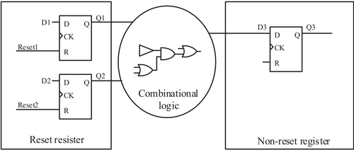
As shown in Figure 4, the outputs of the two registers that need to be reset are Q1 and Q2, respectively. In a normal working circuit in a non-reset state, Q1 and Q2 are passed through the combination logic. Although there is a transient state that exists at the D3 port due to their different arrival delays at the combination logic, their timing still meets the requirements. Therefore, the output of Q3 is normal. However, when the register is reset, due to the sources of reset signals being different, the reset occurs and arrives at different times in the circuit, resulting in Q1 and Q2 not being reset simultaneously. Q1 and Q2, which have thus a certain time difference, are passed through the combination logic to the D terminal in the non-reset register of the next level. They may be sampled by the rising edge of the clock of the non-reset register and transmitted to the Q3 port and thereby generating glitches. Therefore, only the reset control signal cannot solve the problem of glitches or request overflow during the asynchronous reset process. To this end, this work introduces a clamp request control unit, which uses the clamp control logic to clamp the request of low-power components to an invalid state before entering the reset state, ensuring that the system has no overflow of redundant requests, and thus avoiding glitches. Conventional network request clearing approaches basically prevent unintended requests from propagating through the system during power state transitions. They fail to address the glitches caused by asynchronous resets. Similarly, reset isolation units ensure that individual registers reset correctly; however, they lack synchronization across multi-core DSP architectures. This leads to timing mismatches and unexpected transient signals. However, our clamp control unit proactively forces low-power components into an invalid state before executing a reset. Hence, it effectively prevents glitch propagation and ensures a stable transition. Unlike conventional methods, our approach is fully scalable for multi-core DSPs and introduces minimal power overhead. This makes it a more efficient and lightweight alternative.
Afterwards, the clock control unit notifies the clock generation unit to turn on/off the clock signal of the module, orhe power control unit initiates a power state switching command to the module. The clock control unit and power control unit are mainly divided into two types of switching, namely simultaneous switching on/off the clock, power, and storage banks, and simultaneous switching on/off the clock and storage banks. This procedure is implemented by register configuration, making choices during the state switching process.
2.3.2 State Transition Monitoring Module
The state transition monitoring module is responsible for monitoring the process of state transition and determining whether there are any abnormalities during the state transition process. Part of the state transition process needs to be driven by signal jumps, while others are driven by configurable counter counts. There is exception detection during the whole state transition process. When the state transition exception counter meets the conditions and the signal switch is successful, the current state transition will end. The state transition monitoring module mainly includes signal switching controller monitoring, a configurable state transition counter, and an exception detection module.
The power management controller is responsible for controlling the entire chip. For high-speed peripherals, the sampling frequency is high, ensuring stable sampling of control signals from the power management components. For low-speed peripherals such as M1553B, the clock frequency is generally 1 Mbps. It is possible that the power management controller has completed the state switch but has not yet sampled the control signal, resulting in sending incorrect requests and causing chip failure. In order to solve this problem, the power management controller designed in this work includes a configurable state transition counter, which can be configured with different types of clocks counting according to the requirements when performing different types of clock switching. That is, a value that can be adjusted according to the needs (instead of the previous fixed value) is set to avoid the problem of low-speed peripherals getting stuck or high-speed peripherals waiting for too long.
For example, when the counter is configured to a transition state value of 100, it can meet the needs of high-frequency clock modules and successfully complete the state transition. However, for low-frequency modules, this configuration is far from sufficient. During the process of releasing the reset and isolation, the low-frequency module cannot receive the correct signal in a timely manner, which can lead to system disruption. To meet the timing requirements of the low-frequency module, the counter needs to be configured to a count value of 2000. In light of this, setting the counter to a configurable state allows users to flexibly switch the configured count value for each state transition based on the periodic characteristics of different modules through configurable write operations.
2.3.3 Power Supply Control
The power supply control unit is designed to control power delivery to various components of the DSP. It ensures that only the essential modules receive power at any given time. It makes use of power gating to selectively turn off the power supply to high-speed peripherals when not in use. It employs Unified Power Format (UPF) technology to define and control power domains dynamically. It supports independent power domains for each peripheral and prevents unnecessary energy wastage. The power supply is turned on or off based on real-time workload conditions. It implements low-power preservation modes to reduce leakage current when the system is idle. It also ensures minimal power loss during transitions between active and idle states.
2.3.4 Clock Control Unit
The clock control unit is responsible for reducing dynamic power consumption. This is achieved by implementing clock gating techniques. Here, clock signals to inactive modules are disabled to eliminate unnecessary switching power losses. Multi-stage clock control permits fine-grained frequency tunings and enhances power savings while sustaining computational performance. This unit also prevents timing conflicts by synchronizing clock switching operations across different components. This confirms smooth transitions between power states.
2.3.5 Memory Control Unit
Memory management is essential for reducing dynamic and static power consumption. The power management controller applies various techniques to optimize memory usage. The memory control unit specifically enables or disables cache memory banks to optimize energy usage. It implements cache retention modes to preserve essential data and reduce the power consumed by a device. It switches memory between sleep and power-off modes based on real-time access patterns. This unit reduces static leakage power by disabling unused memory banks. It dynamically controls chip selection and power signals to diminish unnecessary power usage.
3 Workflow of Power Consumption Control
Based on the working requirements of the power management controller described above, we design it as shown in Figure 5. The operating status of each component is described as follows:
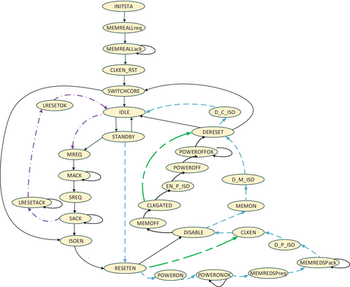
Five states, including INITSTA, MEMREALLreq, MEMREALLack, CLKEN_RST, and SWITCHCORE, are the initial working states of the power consumption controller. After the power reset, the power management controller first completes the repair confirmation of the storage function and then selects the initially enabled modules according to the chip requirements, sequentially turning off the modules that do not need to work. At this time, the entire chip is in a stable, low-power operating state, and the chip begins to work normally.
The IDLE state is idle. When the chip is working normally and there is no need to switch low-power modules, the power consumption controller maintains the currently provided gating control signal and reset enabled signal unchanged. STANDBY status indicates that the power management controller has received a switching command (on or off) to initiate the switching operation.
Nine states, including MREQ, MACK, SREQ, SACK, ISOEN, RESETEN, DISABLE, MEMOFF, CLKGATED, and DERESET, are clock closing processes. First, clear the network requests initiated by the master and slave of the module; Second, in the isolated state, both network request isolation signals and module clamping control signals will be initiated simultaneously; Afterwards, enter the reset, turn off the storage bank, and turn off the clock; Finally, exit the reset control. When the power-off operation is used, after the clock is turned off, three states such as POWEROFF, POWEROFFOK, and ENP_ISO will be switched to complete the power-off control.
The two states, LRESETOK and LRESETACK, are handshake signals provided by the power consumption controller for the modules with other reset type controls (e.g., reset request operations caused by a watchdog), which are used to complete network clearing request operations for modules that require other reset operations.
The seven states of RESETEN, CLKEN, DISABLE, MEMON, D_M-ISO, DERET, and D_P_ISO are the process of turning on the clock. First, the module enters the reset state; next, it turns on the clock and activates the memory storage. Afterwards, it exits the module clamp control state, exits the reset state, and finally enters the module isolation state, and the module works normally. When a power-on operation is required, after resetting, five states including POWERON, POWERONOK, MEMREDSPreq, MEMREDSPack, and D_P_ISO will be conducted to complete the power-on and repair confirmation operation for the module storage bank and then enter the clock-on state.
4 Experimental Results
In this section, the experimental evaluation of the designed power management controller implemented in the FT-xDSP architecture is presented. The experiments were conducted to verify the functionality and effectiveness of the power management strategies under various operational conditions, specifically focusing on the state machine switching processes and power consumption characteristics of the core and peripherals.
4.1 Functional Verification
For FT-xDSP, the functional testing of the designed power management controller is mainly conducted from two aspects: the state machine switching process of the clock power supply and the power supply-off state.
(1) Test the state machine switching process of the clock power supply using a simulation tool from a certain company. After enabling the power management switching process, the waveform is displayed in Figure 6.
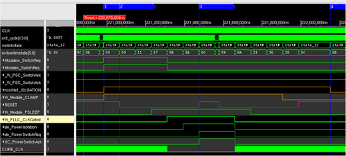
When the ISOLATION (isolation signal) and CLAMP (clamp) signals are activated (at the position of Label 1, which is highlighted in blue color), it indicates that network control has been completed for the module, ensuring the next operation of the module.
Afterwards, the reset control is initiated (at the position of Label 2). After completing the reset, the module is sequentially sent a request signal to turn off the memory bank, clock, and power supply, placing the module in the off state and then exiting the reset control (at the position of Label 3). Then restart the module: first enter the reset state and then turn on the module's power supply, clock, and storage in sequence. After exiting the reset and network isolation (at the position of Label 4), the module will enter the normal working state. The success of turning off and turning on the clock, as well as resetting the module, can be confirmed by displaying the CORE_CLK and RESET waveform signals as shown in Figure 6. When the CORE_CLK signal always displays 0, it indicates that the clock is in the off state; while a square wave pattern with alternating signals of 0 and 1 appears, the clock is in the one state. Moreover, when the RESET signal is 1, it means that the reset has been exited; when the signal is 0, the module enters reset. Whether the closing and opening of the storage bank is successful requires testing with the program code.
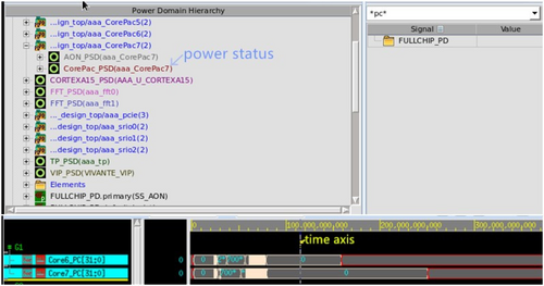
(2) Test the power-off state using a power simulation tool from a certain company to simulate the status of the module. The simulation results will show whether the power control has been successfully realized.
Figure 7 shows that at the beginning of operation, the power supply of the module is in a working state. On the time axis, the power status displays a green circle, indicating that the module is working normally.
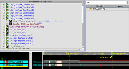
As shown in Figure 8, when the power supply is successfully turned off, the power status displays a red cross on the time axis, indicating that the module has been powered off.
4.2 Analysis of Power Consumption Results
This work conducts a power consumption analysis on the basis of a single core of FT-xDSP to evaluate the actual performance of the power manager, including two aspects: (1) conducting power consumption analysis through power consumption tools before chip fabrication; (2) Analysis of the measured power consumption after chip fabrication.
4.2.1 Pre-Flow-Chip Power Consumption Analysis
Before chip fabrication, the VCD files for a single core in normal working state, clock off state, and power off state are generated respectively. Then, the power consumption reports are obtained by analyzing the VCD files for the above three scenarios, as shown in Tables 2–4.
| 1Power group | Leakage power (mw) | Internal power (mw) | Switching power (mw) | Total power (mw) |
|---|---|---|---|---|
| Clock_network | 0.015 | 2.329 | 15.335 | 17.680 |
| Combinational | 1.517 | 6.556 | 5.250 | 13.322 |
| Sequential | 1.275 | 160.143 | 0.598 | 162. 016 |
| Memory | 1.852 | 0.000 | 0.000 | 1.852 |
| Io_pad | 0.000 | 0.000 | 0.000 | 0.000 |
| Black_box | 0.000 | 0.000 | 0.128 | 0.128 |
| Total | 4.659 | 169.028 | 21.311 | 194.998 |
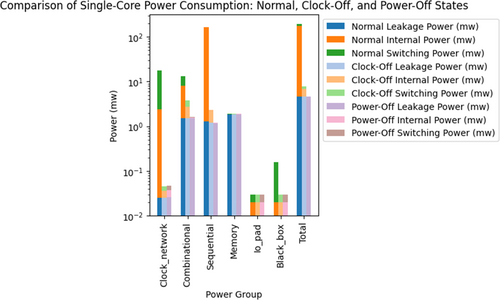
Table 2 shows that the total power consumption of the core during normal operation is 194.998 mw. Among them, the leakage power consumption is 4.659 mw, the internal power consumption is 169.028 mw, and the flip power consumption is 21.311 mw.
Table 3 shows the power consumption status after the core clock is turned off. Compared to the normal working state, the total, leakage, internal, and switching power consumption has decreased by about 95.9%, 1.6%, 98.6%, and 95.27%, respectively.
| Power group | Leakage power (mw) | Internal power (mw) | Switching power (mw) | Total power (mw) |
|---|---|---|---|---|
| Clock_network | 0.015 | 0.001 | 0.000 | 0.016 |
| Combinational | 1.509 | 1.211 | 1.008 | 3.728 |
| Sequential | 1.207 | 1.070 | 0.000 | 2.277 |
| Memory | 1.852 | 0.000 | 0.000 | 1.852 |
| Io_pad | 0.000 | 0.000 | 0.000 | 0.000 |
| Black_box | 0.000 | 0.000 | 0.000 | 0.000 |
| Total | 4.584 | 2.282 | 1.008 | 7.873 |
Table 4 shows that after the core power is turned off, the total, leakage, internal, and switching power consumption is reduced by about 41.4%, 0.8%, 97.91%, and 98.5%, respectively. In Tables 2–4, the normal operating state of the chip refers to the condition in which, after completing kernel transaction processing, the chip remains in a prolonged idle state (i.e., the kernel executes an infinite cycle wait instruction that can only be interrupted by a branch or an interruption in the non-reset condition). The power consumption reduction of 95% after the chip is powered off refers to the power consumption value after the chip's power is turned off, compared to the power consumption in the normal operating state while the chip is in idle mode. The specific data values are highlighted in the Tables 2–4.
| Power group | Leakage power (mw) | Internal power (mw) | Switching power (mw) | Total power (mw) |
|---|---|---|---|---|
| Clock_network | 0.016 | 0.001 | 0.000 | 0.017 |
| Combinational | 1.529 | 0.023 | 0.015 | 1.567 |
| Sequential | 1.150 | 0.018 | 0.000 | 1.168 |
| Memory | 1.852 | 0.006 | 0.000 | 1.858 |
| Io_pad | 0.000 | 0.000 | 0.000 | 0.000 |
| Black_box | 0.000 | 0.000 | 0.000 | 0.000 |
| Total | 4.547 | 0.048 | 0.015 | 4.610 |
The single-core power consumption in the normal, clock-off, and power-off states is collectively illustrated in Figure 9. Power consumption is represented on a logarithmic scale that can make small values more distinguishable, especially when there is a large difference between the smallest and largest values. From Figure 9, It is clearly shown that the total, leakage, internal, and switching power consumption is reduced drastically during the clock-off and power-off states.
4.2.2 Analysis of the Chip Measured Power Consumption
After the chip is taped out, a power consumption tester is used to analyze the power consumption of a single core in different power consumption control states of the chip under different temperature conditions.
Because it is not possible to directly obtain power consumption data for a single core, the incremental testing is adopted, combined with the analysis of power consumption tools from previous simulations, to infer and obtain approximate power consumption data for a single core. Chip test results are shown in Table 5. The meanings of the data in Table 5 are as follows:
| The control state of the core | 25°C Power consumption (mw) | 85°C Power consumption (mw) | 125°C Power consumption (mw) | |
|---|---|---|---|---|
| Power gating status | All cores power off (P1) | 920 | 1725 | 3953 |
| Normal operation condition | Chip + single-core operation (P2) | 1177 | 2056 | 4372 |
| Power consumption reduced by single-core power off (ΔP1) | 257 | 331 | 419 | |
| Consumption reduced ratio by single-core power off (E1) | 21.8% | 16.1% | 9.6% | |
| Clock gating status | Chip + single-core clock gated (P3) | 939 | 1859 | 4271 |
| Power consumption reduced by single-core clock gated (ΔP2) | 238 | 197 | 101 | |
| Consumption reduced ratio by single-core clock gated (E2) | 20.2% | 9.6% | 2.3% | |
1. P1 indicates the idle power consumption of the chip when all cores and peripherals that can be powered off in the chip are turned off after the power-on reset. It is represented by “Chip+” below.
2. P2 represents the power consumption of the chip and single core when turning on its power supply (other core power is off) and clocking and making it in a normal working state;
3. ΔP1 is the difference between P2 and P1, indicating the reduction in power consumption when a single core is turned off.
4. E1 is ΔP1/P2, which indicates the proportion of the power consumption of the chip and a single core compared to the power consumption saved when the core works normally.
5. P3 represents the power consumption after closing the clock of the working core on the basis of P2.
6. ΔP2 is the difference between P2 and P3, indicating the reduced power consumption of a core when the clock is turned off compared to normal operation.
7. E2 is ΔP2/P2, which indicates the proportion of power saved by turning off a core clock compared to the normal operation of the core in the power consumption of the chip and a single core.
4.2.3 Power Consumption Analysis and Comparison
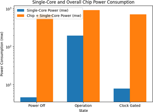
The actual chip test data in Table 4 cannot measure the power consumption of a single core when turned off. In order to estimate the optimization of single-core power consumption in the actual chip, an evaluation analysis of single-core power consumption and full chip power consumption was conducted using a power consumption tool. The results are shown in Table 6. The comparison of power consumption of single-core and single-core with chip is illustrated in Figure 10. Power consumption is represented as a logarithmic scale that can make small values more distinguishable. From Figure 10, it is clearly understood that the ratio of power consumption of single-core with Chip + single-core is high in the operating state.
| 2Type | Single-core power off (mw) | Single-core operation (mw) | Single-core clock gated (mw) |
|---|---|---|---|
| Power consumption of single-core | 4.611 | 194.998 | 7.873 |
| Chip + single-core power consumption (other core power is off) | 697.790 | 921.873 | 705.088 |
| Power consumption ratio of single-core in that of the chip | 0.66% | 21.15% | 1.12% |
The power consumption data analyzed using power consumption tools is usually benchmarked to the actually measured one at 25°C in the chip. Based on the proportion of power consumption of a single core in the overall chip design in Table 6, the actual power consumption of a single core in the chip is calculated proportionally, as shown in Table 7.
| 3Single-core power consumption | 25°C power consumption (mw) |
|---|---|
| Power off | 920 × 0.66% = 6.070 |
| Normal operation | 1177 × 21.15% = 249.000 |
| Clock gated | 939 × 1.12% = 10.520 |
| Reduced ratio by clock gated (E3) | 95.80% |
The red font in Table 6 is an approximate value calculated on the basis of empirical analysis. According to the ratio of the power consumption of a single core to that of the whole chip, the ratio of single-core power consumption in the chip is approximately equal, and then the actual data of the single core is calculated. E3 represents the proportion of power saved by a single core after turning off the clock in the operating power consumption.
On the basis of the data in Table 7, the E3 measurement value of the chip is almost equal to the value obtained by the power analysis tool. Therefore, it can be inferred that using a power controller can reduce power consumption by over 95% at room temperature (25°C). In addition, according to the data analysis at 25°C in Table 5, the power consumption reduction ratio of E1 and E2 is close, and the difference in power consumption saved by turning off the core power and turning off the core clock is not significant. However, when the temperature rises to 85°C, E1 is already much higher than E2; At 125°C, turning off the clock reduces power consumption by only 2.3%, but turning off the power reduces it by about 9.6%. It conforms to the characteristic of static power consumption, which is not significant at room temperature but sharply increases at high temperatures, and also proves that power control can greatly improve the stability of chips by adopting power-off measures at high temperatures.
5 Conclusion
This work proposes an efficient power management controller for DSP that is suitable for multi-core and multi-integrated peripherals. The controller can comprehensively control the power supply, clock, and memory (in the core and high-speed peripheral) of each module in the DSP for turning off and on. When performing power consumption control, it only adopts the clock gating shutdown mode for low-speed peripherals; And for high-speed peripherals and cores, one or both of clock gating and power gating can be used as needed. Moreover, in order to solve the problem of possible glitches during asynchronous reset, a clamp request control unit is introduced in the power management controller to ensure that the system has no overflow of redundant requests. The controller is also set up with a configurable state transition counter, which can adopt different types of suitable clock counting configurations when performing different types of clock switches, to avoid the problem of insufficient state transition time for low-speed peripherals or long waiting time for high-speed peripherals.
The new high-efficiency power control manager demonstrates excellent power management performance. During testing, the power management controller of FT-xDSP reduced power consumption by approximately 95.9% when turning off the gating clock of the core; subsequently, turning off the power of the core reduces the power consumption by 41.4% on the basis of turning off the clock. In the high and low temperature test of the actual chips, it was found that when the temperature reaches 125°C, turning off the power could significantly reduce the power consumption of the chip and ensure its stability.
The power management controller designed in this work is highly fit for the FT-xDSP architecture, which may limit its direct applicability to other DSP architectures. Although the controller functions well in a variety of temperatures, it may not operate at its best in very hot or cold climates. The efficacy of the controller may be limited in all circumstances if the power savings at these extremes—especially in high-temperature scenarios. As we move forward, this power management system can be applied to autonomous vehicles, smart IoT devices, and edge computing applications. AI-based power management approaches can enhance energy optimization by dynamically fine-tuning power states based on workload predictions. In the future, efforts will be made to design the system, which adapts the power management controller to a wider range of DSP architectures, and research could also focus on enhancing the performance of the controller in extreme temperature conditions. Future research could also focus on thermal-aware power management techniques to alleviate overheating issues in high-performance DSPs. Furthermore, the incorporation of quantum-inspired computing can offer new opportunities for energy efficiency enhancements in next-generation DSP architectures.
Author Contributions
Jian Huang: conceptualization, methodology, software, validation, investigation, resources, data curation, writing – original draft, writing – review and editing, visualization. Huili Wang: validation, writing – review and editing. Guohui Gong: supervision, writing – original draft. Lei Wang: validation. Xiaowen Chen: supervision, writing – review and editing, project administration.
Conflicts of Interest
The authors declare no conflicts of interest.
Open Research
Data Availability Statement
The data that supports the findings of this study are available in the Supporting Information of this article.


