Atomic-resolution Interfacial Microstructure and Thermo-electro-magnetic Energy Conversion Performance of Gd/Bi0.5Sb1.5Te3 Composites
Abstract
Thermo-electro-magnetic materials with simultaneously large magnetocaloric (MC) and thermoelectric (TE) effects are the core part for designing TE/MC all-solid-state cooling devices. Compositing MC phase with TE material is an effective approach. However, the elemental diffusion and chemical reaction occurring at the two-phase interfaces could significantly impair the cooling performance. Herein, Gd/Bi0.5Sb1.5Te3 (Gd/BST) composites were prepared by a low-temperature high-pressure spark plasma sintering method with an aim to control the extent of interfacial reaction. The reaction of Gd with the diffusive Te and the formation of GdTe nanocrystals were identified at the Gd/BST interfaces by the atomic-resolution microscope. The formed antisite defects and enhanced {000 l} preferential orientation in BST are responsible for the increased carrier concentration and mobility, which leads to optimized electrical properties. The heterogeneous interface phases, along with antisite defects, favor the phonon scattering enhancement and lattice thermal conductivity suppression. The optimized composite sintered at 693 K exhibited a maximum ZT of 1.27 at 300 K. Furthermore, the well-controlled interfacial reaction has a slight impact on the magnetic properties of Gd and a high magnetic entropy change is retained in the composites. This work provides a universal approach to fabricating thermo-electro-magnetic materials with excellent MC and TE properties.
1 Introduction
The number of air conditioners has proliferated since 2000, having led to a doubling of carbon dioxide emissions.[1, 2] The prevailing cooling technology, vapor-compression refrigeration, has long relied on volatile refrigerants. However, these refrigerants deplete the ozone layer or cause a greenhouse effect thousands of times more severe than carbon dioxide.[3, 4] Therefore, it is of great significance to develop a highly efficient and eco-friendly refrigeration technology. In recent years, all-solid-state cooling technologies without the use of harmful refrigerants, such as thermoelectric (TE) cooling and magnetocaloric (MC) cooling, have attracted considerable attention.[5, 6] TE cooling has wide applications in micro-refrigerator, medical devices, and chip cooling due to its advantages of compact structure, light weight, low noise, and long lifetime.[7-10] The coefficient of performance (COP) for TE cooling is defined as , where TC, TH, and are the cold-side temperature, hot-side temperature, and the averaged figure of merit of a TE material, respectively. The dimensionless figure of merit (ZT) is defined as ZT = α2σT/κ, where α, σ, T, and κ are the Seebeck coefficient, electrical conductivity, absolute temperature, and total thermal conductivity, respectively.[11, 12] High ZT values therefore require materials with high α, high σ, and low κ. Among the various room-temperature TE materials, bismuth telluride (Bi2Te3)-based alloys are the most widely studied TE materials with the best room-temperature TE performance. In the past few decades, numerous methods have been proposed to improve the TE performance of Bi2Te3-based alloys, such as band engineering, defect engineering, nanostructuring, as well as hierarchical architecture approach.[13-18] However, commercial Bi2Te3-based alloys fabricated by zone melting or unidirectional solidification have long been limited to a low ZT of approximately 1.0.[19] To replace conventional vapor-compression refrigeration, the COP of TE cooling must be comparable (around 3.0), and, accordingly, the ZT value of TE material should exceed 2.0.[20] Apparently, it remains extremely challenging to replace conventional vapor-compression refrigeration with TE cooling.
MC cooling is another environmentally friendly refrigeration technology that shows great promise due to its high efficiency, zero emission, low noise, and substantial cooling capacity.[21, 22] The core principle behind MC cooling lies in the cyclic magnetization and demagnetization of MC materials. The curie temperature (Tc), order of magnetic transition, maximum magnetic entropy change (ΔSM), and relative cooling power (RCP) are the important parameters to evaluate the MC performance. The most widely investigated room-temperature MC materials include Gd and its alloys, Gd5(SixGe1-x)4, LaFe13-xSix, MnAs, MnFePxAs1-x, NiMnGa, and MnCoGe, et al.[23-30] Among these materials, Gd is the most commonly used MC material in many active magnetic regenerators due to its sizable ΔSM near room temperature and small magnetic hysteresis.[31] Nevertheless, the inefficient heat exchange between the working fluid and MC material limits the cycle frequency and leads to a low cooling power density.[32, 33] Therefore, it is also extremely difficult to replace vapor-compression refrigeration with MC cooling.
The integration of TE and MC cooling in principle is possible to improve the overall COP of all-solid-state cooling technology. Research of integration originally began with the device level. In 2010, Kitanovski and Egolf proposed an innovative hybrid TE/MC device utilizing TE modules as thermal diodes, enabling a control of heat-flow direction and rate through current manipulation.[33] Soon afterwards, numerical model analysis on the single-state and cascade TE/MC devices was conducted.[34-38] The utilization of TE modules with their swift response and low thermal conductivity has significantly improved the cycle frequency and cooling power density. Nevertheless, the integration of device inevitably brings about additional challenges such as severe heat leakage and Joule heat generated from TE modules.[34, 36] In recent years, the synthesis of La(Fe0.92Co0.08)11.9Si1.1/BST and MnCoGe/BST composites was reported, with emphasis on the potential of realizing an integration of TE and MC cooling on the material level.[39, 40] Their findings highlighted the detrimental impact of the interfacial reaction on the TE and MC performance of composites. Hence, the utmost focus should be placed on the selection of materials and the control of the interfacial reaction between TE and MC materials when designing a high-performance TE/MC composite.
Herein, metallic Gd was selected as the MC phase, and the state-of-the-art room-temperature TE materials Bi0.5Sb1.5Te3 (BST) were selected as the matrix. Gd/Bi0.5Sb1.5Te3 (Gd/BST) composites were synthesized by a low-temperature high-pressure spark plasma sintering (SPS) to investigate the effect of interfacial phase on the MC and TE properties. It was found that GdTe nanostructured phase formed at the Gd/BST interface played a vital role in optimizing the TE properties. The reaction of Te with Gd at the interface consumed overall Te in the BST matrix, resulting in an increase in antisite defects and carrier concentration. The enhanced {000 l} preferential orientation with elevating the sintering temperature (TS) weakened the scattering of carriers and improved the mobility (μ). An increase in phonon scattering due to antisite defects and heterogeneous interfaces reduced the lattice thermal conductivity (κL). Furthermore, the interfacial reaction had a slight impact on the magnetic entropy change (∆S) of composites. The optimized composite sintered at 693 K exhibited a maximum ZT value of 1.27 and a maximum ∆S of 0.104 J·kg−1·K−1, exhibiting their potential in the field of room-temperature TE/MC hybrid refrigeration technology.
2 Results and Discussion
2.1 Phase Constituent and Microstructure
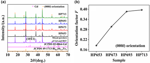
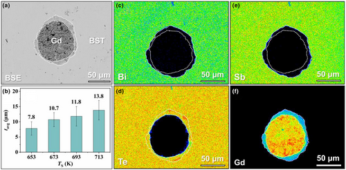
The diffraction peak at around 32° for the mixed powders of Gd and BST is identified as the diffraction peak of the plane in hexagonal Gd. However, it is worth noting that no diffraction peaks of Gd were observed in all the Gd/BST composites. This abnormal phenomenon should be caused by the interfacial reaction between Gd and BST. In order to investigate the interfacial reaction between Gd and BST, a microstructural analysis was conducted with EPMA at the micron scale. Figure 2 clearly shows that the interfacial reaction layer consists of Gd and Te without the trace of Bi and Sb. This phenomenon is consistent with previous findings reported in the literature.[43] Moreover, it was observed that the average thickness (tavg) of interfacial reaction layers gradually increases as the TS increases, increasing from 7.8 to 13.8 μm (Figure 2b). These results suggest that the interfacial reaction range between Gd and BST matrix can be effectively controlled by tuning the TS.
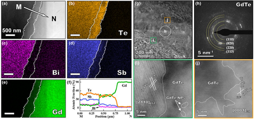
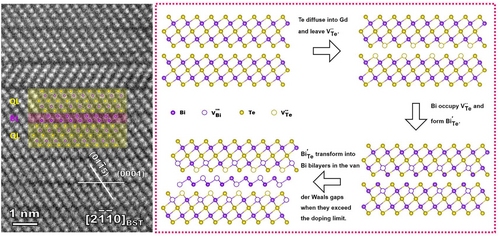
To further investigate the Gd/BST interfacial structures, the microstructures of the heterogeneous interfaces were characterized using scanning transmission electron microscopy (STEM) at the atomic scale. Figure 3a presents that a typical interfacial reaction layer was approximately 500 nm in thickness formed at the interface between Gd (white contrast) and BST matrix (black contrast). The elemental mappings (Figure 3) and energy-dispersive X-ray spectroscopy (EDS) line-scan (Figure 3f) of Te, Bi, Sb, and Gd clearly demonstrate that the interfacial reaction layer consists of Te and Gd at the nanometer scale. Transmission electron microscopy (TEM) image of the Gd/BST interface (Figure 3g) reveals that the reaction layer is composed of many nanocrystals. The corresponding selected area electron diffraction (SAED) pattern can be indexed to the GdTe structure with space group (Figure 3h). The Gd:Te ratio from EDS result is close to 1:1, further confirming that the reaction layer is GdTe. Using atomic-resolution high-angle annular dark field scanning transmission electron microscopy (HAADF-STEM), BST grain along the [20] zone axis, GdTe nanoparticles (NPs), and Gd along the [0001] zone axis can be identified (as shown in Figure 3i,j). Furthermore, the interface between BST and GdTe layer appears relatively smooth, while the interface between Gd and GdTe layer is more irregular. These features indicate that the interfacial reaction is conducted by the diffusion of Te atoms into Gd during the sintering process. The resulted interfacial microstructures should have a large impact on the electrical and thermal transport properties by enhancing the carrier scattering and phonon scattering.[44] In addition, Figure 3i shows a quite amount of BST quintuple layered (QL) structures and Bi (Sb) bilayers (BL) near the Gd/BST interface. It has been reported that Bi (Sb) bilayers generally appear in a Bi (Sb)-rich environment.[45] Herein, the Bi (Sb)-rich environment near the Gd/BST interface is evidently caused by the interfacial reaction between Gd and diffused Te from BST. The evolution mechanism of the Bi (Sb) bilayer structure is illustrated in Figure 4. Weakly bonded Te atoms in Van der Waals gaps tend to diffuse and react with Gd and eventually leave a number of Te vacancies () in BST QL. The Bi (Sb) atoms then occupy these Te vacancies and form cation antisite defects, which possess the lowest formation energy in a Te-poor environment. When the number of antisite defects exceeds the maximum limit, they transform into Bi (Sb) bilayers, which are filled in the van der Waals gaps of BST QLs. These characteristics can be observed in the atomic-resolution HAADF-STEM image of BST as shown in Figure 4. These p-type antisite defects and n-type Bi (Sb) bilayers should have impact on the electrical and thermal transport properties by influencing carrier concentration and enhancing phonon scattering.[45]
2.2 Magnetocaloric Properties
MC cooling is realized by the cyclic magnetization and demagnetization of MC materials based on the MC effect. When the MC materials are magnetized, magnetic moments align in parallel, resulting in a reduction of magnetic entropy (S). This causes the materials to heat up due to an increased lattice entropy under adiabatic conditions. When the MC materials are demagnetized, MC materials absorb heat from the surrounding cooling media under isothermal conditions and MC cooling occurs. Consequently, the magnetic entropy change (ΔS) is a crucial parameter for the MC materials. The maximum ΔS (ΔSM) is typically observed near the Tc as there is a dramatic change in magnetic order.[46] Magnetocaloric properties of Gd and Gd/BST composites are depicted in Figure 5. The M-T thermomagnetic curve suggests that the Tc of Gd is approximately 293 K (Figure 5a). The magnetic phase transition can be determined using the Arrott plot (M2-H/M curves). Based on the Banerjee criterion, a negatively sloped or S-shaped M2-H/M curve near Tc indicates a first-order magnetic phase transition, while a positive slope suggests a second-order magnetic phase transition.[47] In the case of Gd, the Arrott plot displays a positive slope (Figure 5b), which confirms the characteristic of a second-order magnetic phase transition.
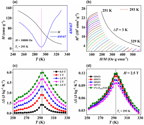
Figure 5c shows that the ΔSM for Gd under 2.5 T is 5.99 J·kg−1·K−1. The RCP is calculated using the equation RCP = ∆SM·δFWHM, where δFWHM is the full-width at half-maximum of the ΔS–T curve.[49] Figure 5d plots the ∆S values of Gd/BST composites and 2%Gd under 2.5 T, while Table 1 summarizes the corresponding MC properties. It is noticeable that the Tc of all Gd/BST composites are approximately 293 K, which is consistent with that of Gd. Furthermore, the ∆SM exhibits a monotonically decreasing trend with increasing TS due to the promotion of interfacial reaction of Gd. The ∆SM of HP713 under 2.5 T is 0.096 J kg−1 K−1, which has a 19% decrease compared to that of HP653. Overall, using the low-temperature high-pressure sintering approach, the MC performance of Gd/BST composites have been well retained.
| Sample | Tc (K) | ∆SM (J kg−1 K−1) | RCP (J kg−1) |
|---|---|---|---|
| HP653 | 293 | 0.118 | 4.93 |
| HP673 | 293 | 0.112 | 4.89 |
| HP693 | 293 | 0.104 | 4.57 |
| HP713 | 293 | 0.096 | 4.26 |
| 2% Gd | 293 | 0.120a | 5.08a |
- The Tc and ∆SM are obtained under applied magnetic field of 0.5 and 2.5 T, respectively.
- a The data is measured ∆SM of Gd after multiplied by 2%.
2.3 Thermoelectric Properties
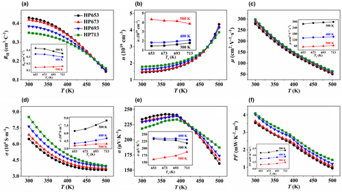
All samples exhibit positive α (Figure 6e), confirming the p-type conduction of Gd/BST composites. This observation is consistent with the Hall measurement results. The Seebeck coefficient (α) first increases as the temperature rises and then decreases due to intrinsic excitation. At room temperature, the α decreases with TS, which results from the increase in n.[53] Figure 6f shows that the PF of the all Gd/BST composites increases steadily with elevating TS. Benefitting from significantly increased σ, the HP713 sample achieves the highest PF of 4.09 mW K−2 m−1 at 300 K.
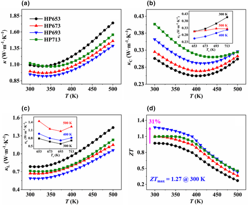
The thermal transport properties and ZT of Gd/BST composites in the temperature range of 300–500 K are displayed in Figure 7. The total thermal conductivity (κ) decreases firstly and then increases with increasing the measuring temperature (Figure 7a). The decrease in κ is attributed to enhanced phonon scattering from lattice vibration, whereas the increase in κ originates from the bipolar thermal effect induced by intrinsic excitation. Figure 7b shows that the carrier thermal conductivity (κC), which is proportional to σ by κC = LσT, also exhibits an increasing trend with TS. The trend of κL is similar to that of κ, as the contribution of κC to κ is small in this work. A higher sintering temperature leads to more antisite defects and heterogeneous interfaces induced by serious interfacial reaction, which can strongly scatter phonons and consequently depress κL.[54] Nonetheless, this effect is counteracted by the reduced phonon scattering stemming from the preferential orientation of {000 l} under the high-temperature sintering condition. Consequently, the κL decreases first and then increases as TS increases. Due to the simultaneous optimization of electron and phonon transport properties, HP693 exhibits a maximum ZT of 1.27 at 300 K, which is 31% higher than HP653 (Figure 7d). In terms of ZT value and ∆SM, this work is superior to previously similar works.[39, 40] The ZT of La(Fe0.92Co0.08)11.9Si1.1/Bi0.3Sb1.7Te3 reached 0.87 at room temperature and ∆SM was only 0.00086 J kg−1 K−1.[39] The ZT of MnCoGe/Bi0.37Sb1.63Te3 reached 0.68 at room temperature and ∆SM was 0.0043 J kg−1 K−1.[40] It demonstrated that the low-temperature high-pressure SPS method used in this work is feasible to obtain both excellent TE and MC properties.
2.4 Cooling Performance
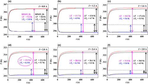
Two single-leg devices with the same dimension of 2.5 mm × 3.2 mm × 11.0 mm were fabricated with HP653 and HP693, which are named as HP653_D and HP693_D, respectively. Figure 8 shows the time-dependence cold-side temperature (TC) and hot-side temperature (TH) of two single-leg devices under different operating currents (I). When a current is applied, both TH and TC undergo an initially rapid change, followed by a gradual approach to the equilibrium. This phenomenon can be attributed to the lag effect caused by Fourier heat and Joule heat. The temperature difference between TH and TC is referred as the working temperature difference (∆T), while the temperature difference between the room temperature TR (300 K) and TC is referred as the cooling temperature difference (∆TC). Both ∆T and ∆TC are used to evaluate the cooling performance of the single-leg device. When the current is lower than the threshold current (2.0 A for HP653_D and HP693_D), both ∆T and ∆TC monotonically increase with the increase of current. However, once the current exceeds the threshold, ∆T continues to increase with the current, while ∆TC gradually decreases. Additionally, when the current exceeds the threshold, ∆TC increases first and then decreases over time. The increase in ∆TC originates from the Peltier effect which enables rapid refrigeration in a short time. The subsequent decrease in ∆TC is attributed to the Fourier heat and Joule heat, which requires more time for heat transport. The time difference between these factors contributes to this phenomenon.[55] Furthermore, under the threshold current, the ∆TC of HP693_D stabilizes at 6.4 K, showing an increment of 12% compared to that of HP653_D. Figure 8 illustrates that both ∆TC and ∆T of HP693_D are greater than those of HP653_D. Therefore, the enhanced ZT value results in enhanced cooling performance. Precise control of TS effectively preserves both the MC effect and TE performance of composites, providing a viable strategy to fabricate thermo-electromagnetic materials with both excellent TE and MC properties for all-solid-state TE/MC hybrid cooling technology. Such TE/MC hybrid cooling technology might overcome the technique barriers as faced by the TE and MC cooling, such as low efficiency, low frequency, low cooling power density, and large heat loss, showing a large potential in the application field of food storage, distribution warehousing, and other refrigeration circumstances.
3 Conclusions
In summary, a series of Gd/BST thermo-electro-magnetic materials had been prepared by a low-temperature high-pressure SPS process. BST grains in the composites exhibit {000 l} preferential orientation. The interfacial reaction layers between Gd and BST formed through the diffusion of Te from BST into Gd. The reaction of Te with Gd at the interface decreases overall Te content in the BST matrix, resulting in an increase in antisite defects and n. The enhanced {000 l} preferential orientation weakened the scattering of carriers and improved the μ. Thus, the σ and power factor of Gd/BST composites increase. The enhanced phonon scattering from antisite defects and interfacial reaction layers leads to a decrease in κL. As a result, the ZT of HP693 reaches the maxima 1.27 and increases by 31%. The maximum ∆TC reaches 6.4 K for HP693_D and increases by 12%. Importantly, all the composites remain the excellent MC performance of Gd. This work provides a universal approach to fabricating a thermo-electro-magnetic material with both TE and MC properties for TE/MC hybrid refrigeration technology.
4 Experimental Section
Sample preparation
The preparation of Gd/Bi0.5Sb1.5Te3 thermo-electro-magnetic material involves several steps. First, high-purity Bi (4 N), Sb (4 N), and Te (4 N) metals were weighted according to the stoichiometry of Bi0.5Sb1.5Te3, with an additional 2% excess of Te. These metals were then sealed in an evacuated quartz tube and melted at 953 K for 6 h in a rocking furnace to obtain a uniformly melted ingot. The ingot underwent a zone melting growth process. Next, the obtained BST ingot was manually crushed and ground into fine powders with particle size below 125 μm. These BST powders were then mixed with commercial Gd balls, which had a diameter of 90–150 μm, in a mass ratio of 98:2 to obtain mixed powders of BST and Gd. To prevent the Gd/BST interfacial reaction, a low-temperature high-pressure SPS method was employed.[56] The mixed powders were finally sintered into a series of Gd/BST composites (SPS-12000-10AT, Shenzhen Xingyuan, China) under a uniaxial pressure of 200 MPa at different temperatures (653, 673, 693, and 713 K).
Structural characterization
The phase constituents of Gd/BST composites were examined using powder X-ray diffraction (XRD, SmartLab, Rigaku Corporation, Japan). Cu Kα radiation (λ = 1.54186 Å) was used as the radiation source. The microstructure and elemental mappings of the Gd/BST interface were characterized using electron probe micro-analyzer (EPMA, JXA-8230, Nippon Electronics Corporation, Japan) equipped with energy-dispersive X-ray spectrometer. The microstructure had been further characterized with a double spherical aberration-corrected transmission electron microscope (TEM, Titan Cubed Themis G2 300, Thermo Fisher, USA). The TEM samples were prepared using focused ion beam (FIB, Helios NanoLab G3 UC, Thermo Fisher, USA).
Property measurements
The transport properties were measured along the same direction perpendicular to the direction of SPS uniaxial pressure. The electrical conductivity and Seebeck coefficient were simultaneously measured using a standard four-probe method (CTA-3, Beijing Cryoall Science and Technology Co., Ltd., China) in a helium atmosphere within the temperature range of 300–500 K. The Hall coefficient was obtained on a self-made device using a modified Hall measurement method.[57] Carrier concentration (n) and mobility (μ) were calculated according to the equations n = |1/RHe| and μ = |σRH|, where e is the electron charge. The total thermal conductivity (κ) was calculated by the equation κ = λρCp, where the bulk density (ρ) was determined by the Archimedes method, the specific heat capacity (Cp) was derived using Dulong-Petit law, and the thermal diffusivity coefficient (λ) was measured by the laser flash method using a Netzsch LFA-467 system. The carrier thermal conductivity (κC) was calculated by the Wiedemann-Franz law κC = LσT, where L is Lorentz constant and was calculated according to the equation L = 1.5 + exp(−|α|/116).[58] The lattice thermal conductivity (κL) was thus obtained by subtracting the electrical contribution from κ according to the relation κL = κ - κC. The magnetic properties were measured using multi-VersaLab vibrating sample magnetometer (VSM, VersaLab, Quantum Design INC., USA). The cooling performance of Gd/BST single-leg cooling devices with 2.5 mm × 3.2 mm × 11.0 mm were measured by a homemade apparatus. A direct power supply (Gwinstek, GPD-2303S) was used to provide the working current. Temperatures at both the ends of single-leg cooling devices were detected by the high-precision T-type thermocouple (OMEGA Engineering INC.) and the data was recorded by the acquisition module and LabVIEW program.
Acknowledgements
This work was supported by the National Key Research and Development Program of China (2019YFA0704903) and National Natural Science Foundation of China (11834012, 52130203, 92163122, 91963207, 91963122).
Conflict of Interest
There are no conflicts to declare.


