Electrospun Semiconductor-Based Nano-Heterostructures for Photocatalytic Energy Conversion and Environmental Remediation: Opportunities and Challenges
Abstract
Harvesting solar energy to drive the semiconductor photocatalysis offers a promising tactic to address ever-growing challenges of both energy shortage and environmental pollution. Design and synthesis of nano-heterostructure photocatalysts with controllable components and morphologies are the key factors for achieving highly efficient photocatalytic processes. One-dimensional (1D) semiconductor nanofibers produced by electrospinning possess a large ratio of length to diameter, high ratio of surface to volume, small grain sizes, and high porosity, which are ideally suited for photocatalytic reactions from the viewpoint of structure advantage. After the secondary treatment of these nanofibers through the solvothermal, gas reduction, in situ doping, or assembly methods, the multi-component nanofibers with hierarchical nano-heterostructures can be obtained to further enhance their light absorption and charge carrier separation during the photocatalytic processes. In recent years, the electrospun semiconductor-based nano-heterostructures have become a “hot topic” in the fields of photocatalytic energy conversion and environmental remediation. This review article summarizes the recent progress in electrospinning synthesis of various kinds of high-performance semiconductor-based nano-heterostructure photocatalysts for H2 production, CO2 reduction, and decomposition of pollutants. The future perspectives of these materials are also discussed.
1 Introduction
The rapid developments of global industry and economy have led to enormous demands for energy.[1-3] According to relevant data,[4-6] the consumption rate of worldwide energy has attained 16.9 TW in 2013 and is estimated to approach 25.6 TW in 2035. In 2017, the primary energy consumption growth has averaged 2.2%, which is up from 1.2% last year and the fastest since 2013.[7] Notably, more than 80% of the used energy comes from fossil fuels such as natural gas, coal, and petroleum.[8] As the fossil fuel consumption decreased in 2020, the greenhouse gas CO2 emissions from the energy use declined by 6.3%, which is the lowest value since 2011.[9] It is not hard to see that the energy shortage and environmental pollution issues are mainly caused by the excessive exploitation and use of non-renewable fossil fuels. Hence, it is an urgent need to develop efficient and low-cost methods for the production of renewable energy and the remediation of contaminated environment. As a promising “green” technology, photocatalysis offers great potential for simultaneously realizing the energy conversion and environmental remediation.[10-15] When a semiconductor photocatalyst is irradiated with the photon energy equal or larger than its band gap, the electrons in the valence band (VB) can be excited to the conduction band (CB) with simultaneous formation of the same amount of holes in the VB.[16-19] The photoinduced electrons on the CB of the semiconductor are capable of reducing water and CO2 for the production of sustainable low-carbon fuels of such H2 and CH4/CO, respectively.[20-26] Meanwhile, the photoinduced holes on the VB of the semiconductor can react with the surface hydroxyl groups to yield OH• radicals, which are a strong oxidizing agent to decompose/mineralize the organic pollutions.[27-31] The photocatalytic oxidation and reduction abilities of semiconductor photocatalysts depend strongly on the redox potentials of their VB and CB, respectively.[6, 32, 33] As shown in Figure 1, the redox potentials of typical photocatalytic reactions for the solar-to-fuel conversion and the pollution decomposition are listed with respect to the VB and CB potentials of different semiconductor photocatalysts.[34-37] This can guide researchers to precisely select the semiconductor photocatalyst for the desired photocatalytic reaction. For instance, achieving the overall water splitting requires that the CB potential of the semiconductor photocatalyst should be more negative than the potential of H+/H2, while its VB potential should be more positive than the potential of O2/H2O.[38-41] Similarly, in order to decompose the organic pollutants effectively, the CB and VB potentials of the semiconductor photocatalyst should enable the photoinduced charge carriers to react with the corresponding chemical groups (O2, OH−, etc.) on the surface of the photocatalyst for producing strong oxidizing radicals (O2•−, OH•, etc.).[42-47] Additionally, the photocatalytic reduction of CO2 over the semiconductor photocatalyst is a proton-assisted multi-electron process, which can generate different kinds of carbohydrate fuels, relying on the CB potential of the photocatalyst in the range from −0.61 to −0.20 V.[48-53] Although various semiconductors have been employed to implement photocatalytic reactions for the purpose of either the energy conversion or the environmental remediation, the photocatalytic efficiencies are still unsatisfactory because of the drawbacks on two aspects:[54-60] I) kinetic processes of the photogenerated charge carriers; and II) microscopic structures and morphologies.
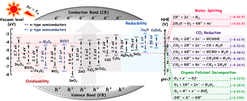
Assembling appropriate semiconductor or metal components into the well-designed semiconductor-based heterostructure is a commonly used strategy for improving the kinetic process of photogenerated charge carriers during the photocatalytic processes.[61-66] In particular, the synergistic integration of various functional nanostructure units into semiconductor-based heterostructure photocatalysts has become the emerging effective strategies to improve the functionality in the research area of energy conversion. Meanwhile, the unique microscopic structure or morphology can also increase the light-harvesting ability, charge separation, and catalytic active site of the photocatalyst.[67-71] For instance, the nanostructured mesoporous photocatalysts possess abundant active sites and short pathways for both the reactant diffusion and the charge carrier transportation;[72-80] the hollow nanostructure can multi-scatter the incident light to increase the light-harvesting efficiency;[62, 81-86] the one-dimensional (1D) nanostructure is beneficial for the photogenerated electron transfer along the photocatalyst;[32, 87-95] the 2D-2D-type semiconductor heterojunction constructed through flat loading one 2D semiconductor onto the other 2D semiconductor surface often leads to high charge mobility and low charge recombination rates.[96-99] Among different nanostructured photocatalysts, 1D semiconductor nanofibers made by electrospinning have more distinct advantages for the potential application in photocatalysis, including processability, 3D open structure, hierarchical porosity, large ratio of length to diameter, high ratio of surface to volume, and small grain sizes.[100-106] In this review, we thoroughly summarize recent progress in the research area of electrospun semiconductor-based nano-heterostructures for the photocatalytic energy conversion and environmental remediation. We highlight structure advantages of electrospun semiconductor-based nano-heterostructure photocatalysts on the increase in the light-harvesting ability, the charge separation, and the catalytic active site. The photoinduced kinetic processes of charge carriers in different electrospun semiconductor-based nano-heterostructure photocatalysts are also understood. The photocatalytic pollutant decomposition, H2 production, and CO2 reduction over electrospun semiconductor-based nano-heterostructure photocatalysts are reviewed, and future perspectives and challenges are discussed.
2 Electrospinning Technique for Photocatalytic Energy and Environmental Materials
2.1 Basic Principles
The earliest information about electrospinning appeared on a patent published by Formhals in 1934. It broadly describes the operation process for producing polymer filaments through electrostatic repulsions between surface charges on the precursor droplet.[107] With the progress of nanoscience and nanotechnology, the electrospinning technique has gained extensive attention in the experimental and theoretical studies. As shown in Figure 2, the key modules of a typical electrospinning setup can be summed up as three parts: 1) high voltage power supply; 2) capillary (including a solution container and a spinneret); and 3) grounded metal collector (usually aluminum foil).[108] The two opposite electrodes on the high voltage power supply are connected with the spinneret and the grounded collector. Usually, the spinneret side filled with the viscoelastic precursor solution of either polymer solution or their melts is applied a high negative voltage with a voltage difference of several tens of kilovolts lower to the grounded collector. During the electrospinning process, the precursor solution can be extruded to form a charged droplet at the nozzle of the spinneret. There are mainly two kinds of electrostatic forces on the droplet: One is the electrostatic repulsion that occurs on the droplet surface due to the existence of like charges; and another one is the Coulombic force between the spinneret and the grounded collector. When the electrostatic repulsion overcomes the surface tension of the droplet, the Coulombic force would drive the ejection of a liquid jet from the nozzle to the grounded collector. This liquid jet experiences fast stretching and whipping processes, thereby deforming into a conical object, the so-called Taylor cone.[109, 110] With the evaporation of the solvent from the stretched liquid jet, the randomly oriented fibers with diameters from tens of nanometers to hundreds of micrometers can be produced. These electrospun fibers interweave with each other, forming a thin fibrous membrane on the collector.[111]
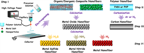
Over the past decades, more than one hundred kinds of natural and man-made polymers, such as water-soluble polyvinyl alcohol (PVA), poly(vinylpyrrolidone) (PVP),[109] and non-water-soluble polyacrylonitrile (PAN), polyimide (PI), and poly(vinylidene fluoride) (PVDF),[108, 115] have been processed into 1D nanofibers by electrospinning. Some of these polymers possess abundant functional groups, which can connect with inorganic metal ions through the coordination interaction. This process kindles the light for electrospinning preparation of inorganic nanofibers by using the organic polymer nanofiber as the structure template. In general, the electrospinning preparation of inorganic nanofibers can be mainly divided into three steps (as shown in Figure 2): 1) addition of metal salts or high-dispersed inorganic nanoparticles into the polymer precursor solution, forming the organic/inorganic mixture solution; 2) electrospinning treatment of the above mixture solution into organic/inorganic composite nanofibers; and 3) calcination of the obtained organic/inorganic composite nanofibers at atmosphere condition to prepare the metal oxide nanofibers. When these metal oxide nanofibers are further calcinated in atmospheres of H2, H2S, and NH3, the corresponding metal, metal sulfides, and metal nitrides can be fabricated, respectively. On the contrary, the metal-free carbon or carbon-based nanofibers can be prepared by carbonizing the electrospun nanofiber of organic polymer that is capable of preparing the carbon material.
2.2 Advantages in Photocatalytic Energy Conversion and Environmental Remediation
In recent years, electrospun semiconductor-based nanofibers have been considered as burgeoning “hot materials” for achieving high-efficient photocatalytic activity toward solar-to-fuel conversion and environmental remediation.[100, 114, 116] According to the literatures,[115, 117-119] the advantages of electrospun nanofiber photocatalysts can be briefly summarized as following aspects (Figure 3): 1) The electrospun semiconductor-based nanofibers possess 3D open hierarchical structures, hierarchical porosity, high surface areas, and large aspect ratios, providing more active sites for the contact with the reactants;[109, 120, 121] 2) the electrospun nanofibers consisting of highly crystalline and closely interconnected semiconductor or metal nanoparticles (NPs) are beneficial for the vectorial transfer of photoinduced charge carriers through the grain boundaries, leading to the high separation efficiency of electron–hole pairs;[122-125] 3) the ultra-long nanofibrous structure enables the electrospun semiconductor photocatalysts to show a light-scattering behavior that can increase light-harvesting in UV region;[126] 4) the components and contents in electrospun semiconductor-based nanofiber photocatalysts could be easily controlled through adjusting the composition of inorganic salts in the electrospinning precursor solutions;[120, 127-130] 5) the electrospun semiconductor-based photocatalysts with a 3D nanofibrous nonwoven web structure can be readily separated from the photocatalytic reaction solution by sedimentation, thereby showing excellent reusable and renewable property;[131-133] and 6) the electrospun semiconductors or carbon nanofibers can serve as active substrates for the assembly of secondary semiconductor nanostructures to fabricate the nano-heterojunction photocatalysts.[100, 116, 134-137] Thus, the design and synthesis of various electrospun semiconductor-based nano-heterostructures is a promising way to solve the poor light-harvesting efficiency, limited catalytic active sites, and fast charge recombination of traditional semiconductor-based photocatalysts on the basis of the photosynergistic effect between the structure advantages of electrospun materials and the kinetic sensitization on the photogenerated charge carriers through engineering the energy band structure in semiconductor-based nano-heterostructures. In this review, we classify newly developed electrospun semiconductor-based photocatalysts as electrospun semiconductor heterojunction photocatalysts, electrospun plasmonic heterostructure photocatalysts, and electrospun flexible heterostructure photocatalysts. The photocatalytic behaviors of the above electrospun photocatalysts for solar-to-fuel conversion and environmental remediation are described, and the corresponding photogenerated charge carriers are also discussed.
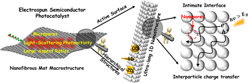
3 Electrospun Semiconductor Heterojunction Photocatalysts
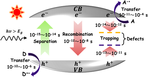
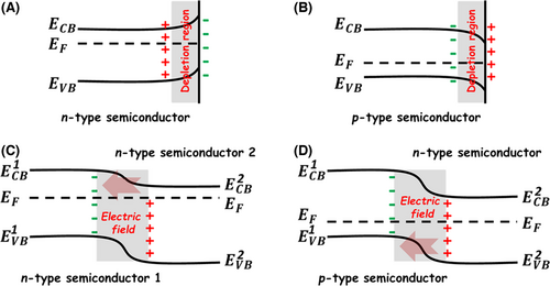
When a semiconductor photocatalyst encounters an intrinsic excitation, vast amounts of charge carriers would generate in its body within the timescale of femtosecond. However, owing to the fast recombination process that occurs in 10−12~10−8 s, most electron–hole pairs are lost in the semiconductor before they migrate to the surface for initiating the photocatalytic oxidation and reduction reactions as shown in Figure 4.[35, 138-143] This phenomenon often leads to a poor photocatalytic efficiency of the single semiconductor photocatalyst. Engineering semiconductor heterojunctions into the photocatalytic system can effectively alleviate the recombination process of photogenerated charge carriers based on the interfacial charge transfer.[87, 144-147] Once the semiconductor heterojunction is formed, an electrostatic field will be built at the hetero-interface due to the interfacial electron transfer from the semiconductor component with higher Fermi level to the semiconductor component with lower Fermi level. This built-in electrostatic field makes the two semiconductor components have opposite charges at their heterojunction region. Consequently, the photogenerated charge carriers can be separated at the semiconductor hetero-interface by the electrostatic interaction.[148-151] This kinetic sensitization process has been widely used to explain the enhanced photocatalytic activities of semiconductor heterojunction photocatalysts, including p-n-type and n-n-type heterojunctions (Figure 5).[152-158]
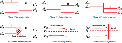
According to the energy band alignment at the hetero-interface of two different semiconductors, the semiconductor heterojunctions can be divided into three types (Figure 6):[159-163] 1) “type I” heterojunction—both the CB and VB of the semiconductor with the smaller band gap are located between those of the semiconductor with the larger band gap; 2) “type II” heterojunction—the CB and VB of the two semiconductors are staggered; and 3) “type III” heterojunction—the VB of one semiconductor lies above the CB of the other semiconductor. Among them, the “type II” heterojunction photocatalyst is the most popular one, since the photogenerated electron and hole can be spatially separated into two different semiconductor components, and therefore strongly restrain their recombination process.[164, 165] Although selecting appropriate semiconductor components to construct the heterojunction photocatalysts can improve the light-harvesting range and the separation of photogenerated charge carriers, the photocatalytic reduction and oxidation abilities inevitably decrease due to the photoinduced interfacial charge transfer. To overcome this drawback, the artificial all-solid-state Z-scheme photocatalytic system is established based on the natural photosynthesis process combined with the fundamental theory of “type II” heterojunction.[166-172] In this specific semiconductor heterojunction photocatalytic system, the electron mediators, such as metal NPs and carbon nanomaterials, are usually introduced between the two semiconductor components to form the Ohmic contact at their hetero-interfaces. Upon interband excitations of these two semiconductor components, the photogenerated electrons at the CB of semiconductor II can transfer to the VB of semiconductor Ⅰ to combine with the photogenerated holes across the electron mediator. In this way, the photogenerated electrons with higher reducibility and the photogenerated holes with higher oxidizability are left in the CB of semiconductor Ⅰ and the VB of the semiconductor II, respectively. This photoinduced kinetic process enables the Z-scheme photocatalytic heterostructure system to show the strong photocatalytic reducibility and oxidizability. Recent research found that the charge separation mechanism of Z-scheme photocatalytic reaction can also occur in many “type II” heterojunction systems without adding the electron mediator, which is a so-called direct Z-scheme photocatalyst.[173-175] The achievement of the direct Z-scheme photocatalyst requires a low potential difference in the CB of semiconductor II to the VB of semiconductor Ⅰ, because this energy band configuration benefits the electron transfer from semiconductor II to Ⅰ at the hetero-interface. It should be pointed that the available photogenerated charge carriers in the Z-scheme photocatalyst is only half of those in the normal “type II” heterojunction photocatalyst under the same reaction conditions due to the existence of charge recombination in the former. Even then, owing to the unique charge transfer mechanism, the Z-scheme photocatalysts still attract much attention in the photocatalytic water splitting to simultaneously produce H2 and O2.[27, 166, 169-173]
As we know, the basic driving force for the interfacial charge separation or recombination is the built-in electric field between the two semiconductor components in their heterostructure. By considering this key factor, a brand-new Step scheme (S-scheme) heterojunction was proposed in the two semiconductor heterostructure system, for which the staggered energy band structure between the two semiconductor components is similar to that of the “type II” heterojunction but with a different charge transfer process.[176] In general, the two semiconductor components in the S-scheme heterojunction should possess a contrary oxidation (with a more positive VB) and reduction (with a more negative CB) abilities. Meanwhile, the Fermi level of oxidation semiconductor component should be lower than that of the reduction semiconductor component. When the well-defined hetero-interface forms between these two semiconductors, the electron on the Fermi level of the reduction semiconductor component would transfer to that of the oxidation semiconductor component across their hetero-interface until a new Fermi level is established. As a result, the built-in electric field directing from the reduction to oxidation semiconductor components forms at their hetero-interface regions, accompanied by the upward and downward shift for the energy band edges of reduction and oxidation semiconductor components, respectively, as shown in Figure 7. The interfacial built-in electric field would drive the transfer of photoinduced electron on the CB of the oxidation semiconductor component to the VB of the reduction semiconductor component for combining with the photoinduced hole on the VB. Thus, the photoinduced electrons on the CB of the reduction semiconductor component and the photoinduced holes on the VB of the oxidation semiconductor components are preserved to initiate the photocatalytic reduction and oxidation reactions, respectively. According to the above introduction, the S-scheme heterojunction is devisable based on the energy band structures and Fermi level of the two semiconductor components. Benefiting from the advantage of the charge transfer process, the S-scheme heterojunction photocatalysts with strong photoredox abilities are suitable for photocatalytic overall water splitting and CO2 reduction.

The design and synthesis of metal–semiconductor-type heterojunctions is another effective strategy to enhance the photogenerated charge separation of the semiconductor-based photocatalysts.[177-182] According to the interface contact between the metal and semiconductor nanostructures, the metal–semiconductor heterojunctions can be classified as Ohmic junction and Schottky junction.[183-188] When the Fermi level of the metal heterocomponent is higher than that of the semiconductor heterocomponent, the electron transfer will take place from the metal to semiconductor heterocomponents to balance the Fermi level of the formed heterojunction system. This electron flow can cause the downward band bending for both the CB and VB of the semiconductor heterocomponent. As a result, the photogenerated electrons transfer from the semiconductor to metal heterocomponents across a potential well formed at the hetero-interface. This type of interface contact in the metal–semiconductor heterojunction is named as “Ohmic junction.”[189-196] On the contrary, when the semiconductor heterocomponent shows an upward band bending due to the electron transfer between the Fermi levels of the metal and semiconductor heterocomponents, an interfacial potential barrier would be built with respect to the photogenerated electron on the CB of the semiconductor heterocomponent. This potential barrier is the well-known Schottky barrier, and the formed heterojunction is called “Schottky junction.” Although the traditional Schottky barrier in the heterojunction impedes the electron transfer from the semiconductor to metal heterocomponents, a number of high-energy photogenerated electrons on the CB of the semiconductor heterocomponent could be still trapped by the metal heterocomponent across the Schottky junction area.[197-205] Thus, the metal heterocomponent in metal–semiconductor-type heterojunctions often serves as the “electron sink” to promote the photogenerated charge separation. In the case of photocatalytic H2 production reaction, many noble metal nanostructures, such as Au, Ag, Pt, and Pd, also act as efficient cocatalysts, which can not only promote the photogenerated charge separation but also lower down the overpotential for H2 production.[2, 206-208] Among these noble metal cocatalysts, Pt nanoparticle has received much concern due to its small work function and low H2 overpotential.[209-214] Unfortunately, the use of noble metal cocatalysts usually suffers from stiff price and earth rarity. In recent years, much effort has been devoted to the development of low-cost and earth-abundant nanomaterials to replace the expensive noble metal cocatalysts for boosting photocatalytic water splitting or reduction.[215, 216] The metal-like carbon nanostructures, such as nanotubes (NTs), nanofibers, quantum dots (QDs), and ultra-thin nanosheets (NSs) (graphene), are effective metal-free cocatalysts for assisting H2 production.[217-225] The contact type of the hetero-interface between these carbon nanomaterials and semiconductors generally belongs to either “Ohmic junction” or “Schottky junction.”[31, 226-228] In this regard, the photoinduced charge separation mechanism of carbon–semiconductor heterostructures is the same as that of metal–semiconductor-type heterojunctions.
3.1 Homogeneous Semiconductor Heterojunction Nanofibers
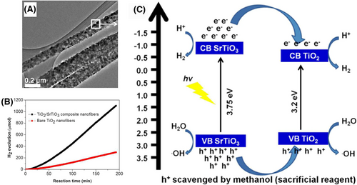
The homogeneous semiconductor heterojunction nanofibers mean that two or more kinds of semiconductor NPs with definite heterojunction interfaces are randomly dispersed into the electrospun nanofibers. This type of heterojunction nanofibers can be easily obtained through simultaneously adding diverse metal salts into the polymer precursor solution during the electrospinning fabrication process for inorganic nanofibers. The large number of semiconductor heterojunction units formed into the electrospun nanofibers could not only boost the photogenerated charge separation of semiconductors but also increase contact interfaces between semiconductors and reactants. As a result, a high-efficient photocatalytic activity would be expected on homogeneous semiconductor heterojunction nanofibers. The TiO2/SrTiO3 composites in the electrospun nanofibers belong to the “type II” heterojunction, which exhibit a higher photocatalytic H2 production rate over bare TiO2 nanofibers in a water/methanol sacrificial reagent system under the irradiation of UV light.[229] In this system, the photogenerated electrons and holes transfer from the SrTiO3 to TiO2 heterocomponents, which lead inevitably to the charge carrier recombination in TiO2 (Figure 8). From the viewpoint of photoinduced charge separation, the design and synthesis of homogeneous semiconductor “type II” heterojunction nanofibers are welcome in the areas of photocatalytic organic pollution treatment and H2 evolution. The electrospun nanofibers of CeO2-ZnO, TiO2-ZnO, SnO2/ZnO, and BiOCl/Bi2Ti2O7 heterojunctions are abided by the charge separation process of “type II” heterojunctions upon UV light irradiation.[230-234]
To extend the light-harvesting region, many narrow band-gap semiconductors, such as Bi2WO6, Fe2O3, SnS2, Bi2MoO6, InVO4, BiVO4, BiFeO3, BN, and graphitic carbon nitride (g-C3N4), are usually employed as the heterocomponents to construct the homogeneous “type II” heterojunction nanofibers.[235-239] The ZnO/Bi2WO6 nanofibers consisted of nanosheets (NSs), and NPs could be synthesized using a straightforward strategy combining an electrospinning technique with sintering process. These electrospun nanofibers not only possess more active sites but also can effectively restrain the recombination of photoinduced electron/hole and therefore exhibit excellent photocatalytic and recycle properties for the decomposition of RhB and methylene blue (MB) dyes under UV-visible light irradiation.[240] When integrating visible light-active “type II” heterojunctions, that is, α-Fe2O3/Bi2MoO6 and α-Fe2O3/Bi2WO6, carbon-doped TiO2/carbon, BiVO4/Bi4V2O11, into the electrospun nanofibers, the photocatalytic activity of the formed homogeneous semiconductor heterojunction nanofibers can be further enhanced due to the improved light absorption and utilization abilities.[241-245]
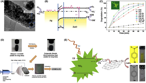
Many homogeneous noble metal/semiconductor heterojunction nanofibers can be prepared by a simple electrospinning process, followed by heat treatment to remove polymer templates and simultaneously to convert noble metal salts into noble metal NPs.[246] By using this synthesis route, the Ag-ZnO homogeneous heterojunction nanofibers with a diameter of 80–150 nm and coupled Ag NPs in the size ranging from several to 15 nm have been achieved. The optimal photocatalytic activity of Ag-ZnO homogeneous heterojunction nanofibers for RhB decomposition exceeds that of pure ZnO nanofibers by a factor of more than 25. This enhanced photocatalytic activity is attributed to the formation of “Ohmic junction” at the Ag-ZnO interface, which promotes the charge separation, thereby allowing both the photogenerated electrons and holes to participate in the overall photocatalytic reaction (Figure 9A–C).[247] The electrospinning preparation of graphene/Pd/TiO2 multi-heterojunction nanofibers can further increase the photocatalytic activity due to the existence of new electron acceptor of graphene to accelerate the photogenerated charge separation. The photocatalytic decomposition efficiency of 4-NP was nearly 100% over the graphene/Pd/TiO2 heterojunction nanofibers under visible light irradiation (Figure 9D,E).[248]
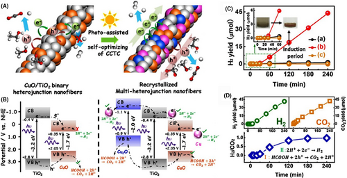
Over the past years, the CuO-based homogeneous heterojunction nanofibers have attracted much attention in the research field of photocatalysis.[249-256] Among them, the mechanism of CuO/TiO2-based nanofibers during the photocatalytic process is very interesting. The energy band structure at the CuO/TiO2 interface follows the “type I” heterojunction. This means that both the photogenerated electrons and holes transfer from the TiO2 to CuO heterocomponents, leading to the improved charge separation of the TiO2 heterocomponent.[249] However, from the viewpoint of the thermodynamic principle, the photogenerated electrons on the CuO surface are not suitable for the photocatalytic proton reduction, because the CB potential of CuO is situated below the reduction potential of H+/H2 (~−0.42 V). Zhang et al. demonstrated that upon simulated sunlight irradiation, the electrospun binary CuO/TiO2 heterojunction nanofibers can be recrystallized to form the quaternary Cu/Cu2O/CuO/TiO2 multi-heterojunction nanofibers due to the kinetic difference of the exciton migration during the photocatalytic process. The rate constant of interfacial electron transfer in the quaternary nanofibers (~1.7 × 10⁸ s−1) is much higher than that of the binary ones (~0.7 × 10⁸ s−1). As a result, a 40-fold enhanced H2 production rate was observed on the recrystallized nanofiber photocatalyst during the photocatalytic decomposition of formic acid as compared to the pure TiO2 nanofibers (Figure 10).[253] Interestingly, by adjusting the electrospinning parameter, the semiconductor-based multi-heterojunctions with specific nanostructures, such as mesoporous, nanobelts (NBs), or NTs, can be obtained, which possess superior photocatalytic activity due to the improved separation of photogenerated charge and the unique nanostructure property.[235, 257-259] Some briefly comparison of the photocatalytic activities for different homogeneous semiconductor-heterojunction nanofibers can be seen in Table 1.
| Photocatalyst | Heterojunction type | Mass | Incident light source | Conditions | Time | Activity | Refs |
|---|---|---|---|---|---|---|---|
| TiO2/SrTiO3 | I | 1 g/L | UV/400 W/Hg lamp | methanol (aq)/10% |
200 min |
H2/1100 μmol | [ 229 ] |
| TiO2/CuO | I | 5 mg | UV-Vis/300 W/Xe lamp | methanol (aq)/10 mL/10% | -- | H2/1146.9 μmol·g−1·h−1 | [ 251 ] |
|
MO (aq)/15 mL/20 mg·mL−1 +0.5 mL of H2O2 |
60 min | 100% | |||||
| CuO/TiO2 | I | 25 mg | UV-Vis/300 W/Xe lamp |
RhB (aq)/50 mL/5 × 10−5 M +2 mL of H2O2 |
30 min | 100% | [ 249 ] |
| Vis/300 W/Xe lamp /λ > 420 nm | 80 min | 100% | |||||
| CuO-Co3O4/N-TiO2 | II | 5 mg | Vis/300 W/Osram lamp | MB + MO (aq)/5 mL/30 mg·L−1/pH = 10 | 1 h | 100% | [ 391 ] |
| Au/CuO/Co3O4 | Schottky | 10 mg | Vis/100 mW/Xe lamp | Na2S2O8 + NaOH (aq)/10 mL/0.1 M + 1 M/pH = 8.8 | -- | O2/2.92 mmol·h−1·g−1 | [ 259 ] |
| Ag/ZnO | Ohmic | 10 mg | UV/8 W/low-pressure Hg tube/254 nm | RhB (aq)/10 mL/2.5 × 10−5 M/pH = 5.4 | 50 min | 100% | [ 247 ] |
| CdS/ZnO | II | 50 mg | Vis/Enviolet GmbH, Karlsruhe, Germany | MB (aq)/100 mL | 100 min | 90% | [ 392 ] |
| TiO2/ZnO | II | 1 mg | UV/6 W/312 nm | S. aureus grown in LB media/37 °C/24 h/1 × 104 CFU·mL−1 | 30 s | 86.7% | [ 393 ] |
| ZnO/TiO2 | II | 1 mg/mL | Vis/75 W/Xe lamp/λ > 400 nm | MB (aq)/15 ppm | 125 min | 95.82% | [ 232 ] |
| SiO2/TiO2 | II | 20 mg | full sunlight/500 W/Xe lamp | MO (aq)/30 mL/40 mg·L−1 | 120 min | 94% | [ 394 ] |
| ZnO/Bi2WO6 | II | 60 mg | Simulated solar/350 W/Xe lamp | RhB (aq)/40 mL/10 mg·L−1 | 2.5 h | 90.4% | [ 240 ] |
| MB (aq)/40 mL/20 mg·L−1 | 70 min | 91.6% | |||||
| α-Fe2O3/Bi2MoO6 | II | 100 mg | Simulated sunlight/500 W/Xe lamp | MB (aq)/40 mL/20 mg·L−1 | 4 h | 90.7% | [ 241 ] |
3.2 Hierarchical Semiconductor Heterojunction Nanofibers
Hierarchical semiconductor heterojunction nanofibers can be synthesized through assembling the secondary semiconductor or metal nanostructures onto the electrospun nanofibrous substrates. In this type of heterostructure photocatalysts, an elaborate design of the secondary nanostructures on the electrospun nanofibrous substrates is conducive to increase the light absorption, interfacial charge transfer, and surface active site, therefore leading to the enhanced photocatalytic activity (Figure 11). In general, TiO2 and carbon materials are widely used as the nanofibrous substrates to be decorated by other nanostructures. This is because that TiO2 is a classical photocatalyst with good chemical stability, while the carbon nanofiber is a good conductor to trap the photogenerated electron from the cohesive semiconductors. Many semiconductor nanostructures have been loaded onto the electrospun TiO2 or carbon nanofibers to enhance the UV or visible light photocatalytic activities.
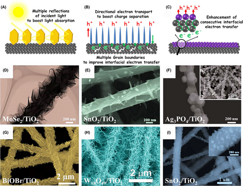
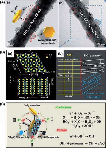
Visible light-active sulfide nanostructures, such as SnS2 NSs, ZnIn2S4 NSs, CdS NSs, NiS NSs, and MoS2, are frequently chosen as the hierarchical heterojunction components for improving both the light-harvesting region and the charge carrier separation of the electrospun TiO2 nanofibers.[260-264] A low lattice mismatch between the two semiconductor heterocomponents is a prerequisite condition to obtain the hierarchical semiconductor heterojunction nanofibers. Zhang et al. found that by using a simple hydrothermal method, the single-crystalline SnS2 NSs with ultra-thin 2D layered nanostructures (4–8 nm) could be uniformly lying flat on the electrospun TiO2 nanofibers consisted of anatase–rutile (AR) mixed-phase TiO2 NPs. The flat-lying growth of the SnS2 NSs on the TiO2 nanofibers’ surface is ascribed to low lattice mismatch values of the ()SnS2/(101)TiO2(anatase) hetero-interface (3.3%) and the ()SnS2/(110)TiO2(rutile) hetero-interface (2.7%). Photocatalytic tests indicate that the hierarchical SnS2/TiO2 (anatase–rutile) nanofibers as the tricomponent heterojunction system possess the stronger photocatalytic activity than the bicomponent heterojunction system of hierarchical SnS2/TiO2 (anatase) nanofibers or TiO2 (anatase–rutile) nanofibers. This suggests that the three-way photosynergistic effect between SnS2, TiO2 (anatase), and TiO2 (rutile) components in the multi-component heterojunction nanofibers results in the high separation efficiency of photogenerated electron–hole pairs (Figure 12).[260]
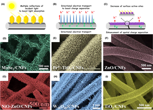
Electrospun carbon nanofiber is a kind of low-cost electron acceptor, which can effectively boost the photogenerated charge separation of semiconductor photocatalysts (Figure 13). When using the electrospun carbon nanofibers as the substrates for constructing the hierarchical semiconductor heterojunction nanofibers, the surface of carbon nanofibers should be firstly activated by nitric acid or plasma. The as-activated carbon nanofibers possess abundant active sites for allowing the hydro/solvothermal assembly of the secondary multi-functional semiconductor nanostructures, such as ZnO NPs, TiO2 NPs, bismuth oxychloride NSs, MoSe2, and NSs.[265-272] As an instance, CuS NPs/ZnO NR heterostructure arrays have been grown on electrospun carbon nanofibers by a simple combination of a hydrothermal process and successive ionic layer adsorption and reaction. Upon simulated solar light irradiation, the photocatalytic activity of CuS/ZnO/carbon heterostructure nanofibers for MB decomposition is 2.2 times higher than that of ZnO. This enhanced photocatalytic activity is ascribed to the broadened light absorption range and improved charge carrier separation, mainly arising from the cooperative effect of the “type II” heterojunction at CuS/ZnO interface and conductive carbon nanofibers.[272]
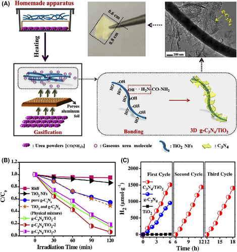
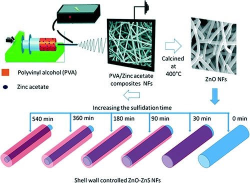
Besides the hydro- or solvothermal synthetic route, the hierarchical semiconductor heterojunction nanofibers can be also obtained through the decoration of semiconductor nanostructures onto electrospun nanofibers by other techniques, such as vapor transport deposition, photoreduction, wet-chemical assembly, and in situ sulfidation.[273-280] Ghosh et al. produced a set of hierarchical “NRs-on-NFs” mesoporous heterostructures through high-temperature organization of V2O5 NRs-on-TiO2 nanofibers for enhancing the photocatalytic activity of ethanol oxidation under visible light irradiation.[281] Zhou et al. decorated electrospun TiO2 nanofibers with g-C3N4 NSs to form “type II” heterojunction via a facial gas–solid reaction. The specific surface area of the obtained g-C3N4/TiO2 heterojunction nanofibers could reach 121.5 m2 g−1. Upon visible light irradiation, the rate constant decomposition (RhB) and the H2 evolution rate of the hierarchical heterojunction nanofibers are 4.6 and 1.6 times of g-C3N4 NSs, but 23 and 167.8 times of TiO2 nanofibers, respectively (Figure 14).[282] Uyar and co-workers prepared the ZnO-ZnS core–shell heterojunction nanofibers via electrospinning followed by sulfidation process. During the sulfidation process, the surface of electrospun ZnO nanofibers can be in situ-converted into the ZnS NPs with the thickness from 5 to 50 nm depending on the sulfidation reaction time from 30 to 540 min. Owing to the matchable energy band configuration between ZnO and ZnS, the hierarchical ZnO-ZnS heterojunction nanofibers exhibited high photocatalytic activities for both RhB and 4-NP decompositions under UV and visible light irradiation (Figure 15).[283] In Table 2, we also summarized some typical examples of hierarchical semiconductor-heterojunction nanofibers as photocatalysts for photocatalytic energy conversion and environmental remediation.
| Photocatalyst | Heterojunction type | Mass | Incident light source | Conditions | Time | Activity | Refs |
|---|---|---|---|---|---|---|---|
| SrTiO3 cubes/TiO2 NFs | I | 100 mg | UV/Upland UVP lamp/254 nm | AO 7 (aq)/60 mL/50 mg·L−1 | -- | ~99% | [ 395 ] |
| Ag2O NPs/BiVO4 NFs | II | 5 mg | Vis | RhB (aq)/10 mg·L−1 | 100 min | 98.47% | [ 396 ] |
| TiO2 NFs@BiOI NSs | II | 20 mg | Vis/500 W/Xe lamp/λ > 420 nm | RhB (aq)/20 mL/20 mg·L−1 | 135 min | 92% | [ 397 ] |
| BiOCl NSs/TiO2 NFs | II | 10 mg | UV/300 W/Xe lamp | RhB (aq)/100 mL/5 mg·L−1 | 15 min | 96.9% | [ 398 ] |
| BiOBr NSs/TiO2 NFs | II | 10 mg | UV/50 W/high-pressure Hg lamp/313 nm | RhB (aq)/100 mL/10 mg·L−1 | 20 min | 89% | [ 386 ] |
| MO (aq)/100 mL/10 mg·L−1 | 20 min | 95% | |||||
| 100 mg | Vis/150 W/Xe lamp/λ > 400 nm | RhB (aq)/100 mL/10 mg·L−1 | 1 h | 94% | |||
| CdS NRs/TiO2 NFs | II | 8 mg | Vis/300 W/Xe lamp/λ > 420 nm |
Benzotrifluoride (oxygen-saturated)/1.5 mL +alcohol (molecular oxygen 0.1 MPa)/0.1 mmol |
4 h |
benzyl alcohol: conversion ~22% selectivity ~99% |
[ 279 ] |
| MoO3 NSs/TiO2 NFs | II | 10 mg | UV/50 W/Hg lamp/313 nm | RB (aq)/100 mL/10 mg·L−1 | 40 min | 97% | [ 399 ] |
| MoSe2 NSs/TiO2 NFs | II | 25 mg |
Full spectrum Source/300 W/Xe lamp/320–2500 nm |
RhB (aq)/50 mL/10 mg·L−1 | 40 min | ~98% | [ 384 ] |
| 25 mg | TC (aq)/50 mL/10 mg·L−1 | 2 h | ~91% | ||||
| 30 mg | Cr(VI)/30 mL/50 mg·L−1/pH = 3 | 2 h | ~95% | ||||
| TiO2 NRs/SnO2 hollow NFs | II | 50 mg | UV/15 W/Hg lamp/254 nm | RB5 (aq)/100 mL/30 mg·L−1 | 3 h | ~100% | [ 400 ] |
| g-C3N4 NSs/TiO2 NFs | II | 50 mg | Vis/500 W/Xe lamp/420–780 nm | RhB (aq)/50 mL/10 ppm | 2 h | 93.6% | [ 282 ] |
| 100 mg | Vis/300 W/Xe lamp/420–780 nm |
methanol (aq)/100 mL/10% + H2PtCl6 alcohol solution/20 μL/50 g·L−1 |
-- | H2/251.7 μmol·h−1·g−1 | |||
| TiO2 NFs/graphdiyne NSs | Ohmic | 0.1 mg | UV/2 W·cm−2/Hg lamp/365 nm | RhB (aq)/1 mL/8 μg·mL−1 | 1 h | ~90% | [ 401 ] |
| 0.1 mg/mL | MRSA cells/20 mL liquid LB medium/109 CFU·mL−1 | 5 min | 98% |
3.3 Z-Scheme Semiconductor Heterojunction Nanofibers
Recent studies found that many homogeneous semiconductor heterojunction nanofibers obey the direct Z-scheme charge transfer mechanism after interband excitations of the semiconductor components.[284-287] This kind of Z-scheme semiconductor heterostructure nanofibers has been investigated in photocatalytic pollution decomposition, H2 production, and CO2 reduction.[284-287] Xu et al. developed a simple and effective method for fabricating anatase and rutile biphase TiO2 nanofibers with controllable rutile content via different cooling speeds (slow cooling and rapid cooling) of calcined electrospun TiO2 nanofibers. Upon UV light irradiation, the photogenerated electrons on the CB of anatase TiO2 can transfer to the VB of rutile TiO2, therefore prolonging lifetimes of photogenerated electrons and holes on the rutile and anatase TiO2, respectively, for fulfilling the photocatalytic reduction and oxidation reactions. This is the first time to report the Z-scheme photocatalytic mechanism for enhancing the photocatalytic activity of electrospun anatase–rutile biphase TiO2 nanofibers for H2 production.[288] Zhang et al. propose that the direct Z-scheme photocatalytic mechanism also occurs in electrospun WO3/TiO2 heterojunction nanofibers. Interestingly, after loading photocatalytic sensitizers of such MoS2 NS, Pt NPs, and carbon layers on the surface of WO3/TiO2 heterojunction nanofibers, the photogenerated charge carriers in the obtained ternary heterojunction system can be further separated, thereby leading to the enhanced photocatalytic activity for H2 production as compared to traditional Z-scheme WO3/TiO2 nanofibers. This is a smart strategy to combine the Z-scheme charge transfer with the semiconductor-based heterojunction effect (Schottky junction, “type II” heterojunction, and LSPR effect) for synergistically enhancing the photocatalytic H2 production.[287, 289-291]
3.4 S-Scheme Semiconductor Heterojunction Nanofibers
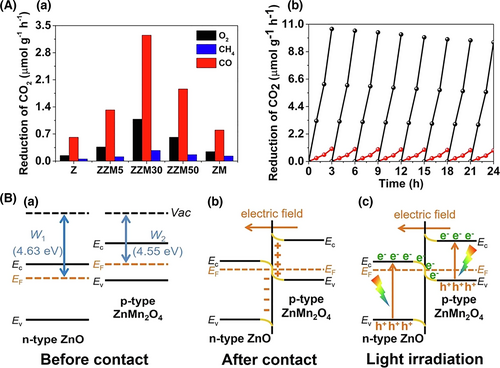
Since the Step scheme (S-scheme) heterostructure was first proposed by Yu’s group in 2019,[176] this kind of heterojunction concept has been widely investigated in the research area of low-dimensional semiconductor heterostructure-based photocatalysis, in especial, for the electrospun semiconductor-based heterostructure nanofibers.[292-297] For instance, Wang et al. reported a series of sulfur-doped g-C3N4/TiO2 S-scheme photocatalysts for Congo Red degradation under simulated solar light irradiation. The photocatalytic performance of the composite NFs is much higher than that of pure TiO2 and sulfur-doped g-C3N4. The enhanced photocatalytic activity is attributed to the S-scheme heterojunction mechanism.[293] Deng et al. fabricated a p-type ZnMn2O4/n-type ZnO S-scheme heterojunction nanofiber by in situ-grown ZnMn2O4 on ZnO NFs via electrospinning and thermal calcination. The obtained composite NFs were used for photocatalytic CO2 reduction under visible light irradiation. The production rates of CO and CH4 were greatly improved in the ZnMn2O4/ZnO NFs compared with those in pristine ZnO NFs and ZnMn2O4. This work firstly realized an S-scheme heterojunction composed of p-type and n-type semiconductors (Figure 16).[294] Table 3 shows the comparison of photocatalytic activities for different electrospun semiconductor-heterojunction nanofibers based on Z-scheme or S-scheme.
| Photocatalyst | Heterojunction type | Mass | Incident light source | Conditions | Time | Activity | Refs |
|---|---|---|---|---|---|---|---|
| α-Fe2O3/FeVO4 homogeneous NFs | Z-scheme | 100 mg | Vis/500 W/Xe lamp/λ > 400 nm | MB (aq)/100 mL/20 mg·L−1 | 3 h | 97.5% | [ 402 ] |
| BiFeO3/Bi2Fe4O9 homogeneous NFs | Z-scheme | 100 mg | Vis/300 W/Xe lamp/λ > 420 nm | TEOA (aq)/100 mL/10% | 8 h | H2/800 μmol·g−1 | [ 284 ] |
| 50 mg | Vis/350 W/Xe lamp/λ > 400 nm | RhB (aq)/50 mL/10 mg·L−1 | 2 h | 65% | |||
| Anatase–rutile TiO2 homogeneous NFs | Z-scheme | 50 mg | UV/350 W/Xe lamp |
Methanol (aq)/80 mL/20%/ +H2PtCl6·6H2O (aq) (0.6 wt% Pt) |
-- | H2/324 μmol·h−1 | [ 288 ] |
| NiS/TiO2 core–shell NFs | Z-scheme | 50 mg | UV-Vis/350 W/Xe lamp | Methanol (aq)/80 mL/20% | -- | H2/655 μmol·g−1·h−1 | [ 263 ] |
| Carbon-coated TiO2/WO3 homogeneous NFs | Z-scheme | 20 mg | UV-Vis/300 W/Xe lamp | Methyl alcohol (aq)/70 mL/36% | -- | H2/~1570 μmol·g−1·h−1 | [ 287 ] |
| TiO2/g-C3N4/RGO homogeneous NFs | Z-scheme | 50 mg | Simulated solar/500 W/Xe lamp | RhB (aq)/50 mL/10 mg·L−1 | 60 min | 99.1% | [ 403 ] |
| CuAl2O4 hollow NFs/Bi2WO6 NSs | Z-scheme | 50 mg | Vis/300 W/Xe lamp/λ ≧ 420 nm/150 mW·cm−2 | H2O/50 mL | -- |
H2/17.8 μmol·g−1·h−1 O2/5.8 μmol·g−1·h−1 |
[ 404 ] |
| Vis/150 W/Xe lamp/λ ≧ 420 nm/80 mW·cm−2 | RhB (aq)/50 mL/10 mg·L−1 | 70 min | 97.85% | ||||
| MO (aq)/50 mL/10 mg·L−1 | 100 min | 96.55% | |||||
| 4-NP (aq)/50 mL/10 mg·L−1 | 150 min | 94.66% | |||||
| TaON/Bi2MoO6 NSs core–shell NFs | S-scheme | 40 mg | Vis/300 W/Xe lamp/λ > 400 nm/97 mW·cm−2 | Levofloxacin antibiotic (aq)/100 mL/20 mg·L−1/pH = 6.2 | 75 min | 92.7% | [ 405 ] |
| Cr(VI) (aq)/100 mL/20 mg·L−1/pH = 5.1 | 75 min | 82.8% | |||||
| TiO2/CdS homogeneous NFs | S-scheme | -- | UV-Vis/350 W/Xe lamp | Methyl alcohol (aq) | -- | H2/2320 μmol·g−1·h−1 | [ 406 ] |
| Bi2O3 NPs/TiO2 NFs | S-scheme | 50 mg | Vis/Xe lamp | Phenol (aq)/15 mL/100 mg·L−1 | 120 min | 45% | [ 407 ] |
4 Electrospun Plasmonic Heterostructure Photocatalysts
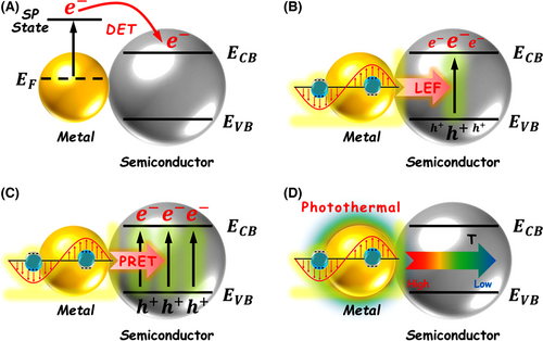
From viewpoints of light absorption and utilization, noble metal nanostructures (i.e., Ag, Au, Pt, Pd) are better candidates for sensitizing semiconductor photocatalysts because of their localized surface plasmon resonance (LSPR).[178, 298-302] LSPR refers to the resonant photon-driven collective oscillation of free electrons in noble metal nanostructures.[303, 304] This fascinating near-field effect enables noble metal nanostructures as the “optical antenna” to strongly absorb and concentrate incident phonons at their plasmon resonance frequency.[305, 306] Furthermore, resonance excitation of noble metal nanostructures can generate plasmonic “hot spots” to greatly enhance localized electric fields on the near surface (<10 nm) of the nanostructures. Notably, the plasmon resonance wavelength of noble metal nanostructures can be tuned, ranging from ultraviolet (UV) to visible, and even to near-infrared (NIR) region, by adjusting parameter conditions, including the metal species, metal morphology, and surrounding medium.[185, 307, 308] Thus, coupling noble metal nanostructures with semiconductors to form plasmonic photocatalysts has become a promising tactic to enhance the photocatalytic activity thanks to LSPR property of noble metal nanostructures. To date, four basic mechanisms have been proposed to explain the plasmon-enhanced photocatalytic activity over noble metal-decorated semiconductor nanostructures (Figure 17): 1) direct “hot electron” transfer (DET)—the LSPR-excited “hot electrons” of the noble metal nanostructure can reach a high-energy surface plasmon state, and then transfer directly into the CB of the semiconductor nanostructure that is in intimate contact with the noble metal nanostructure;[203, 309-315] 2) local enhancement of electric field (LEF)—the LSPR excitation of noble metal component in the noble metal–semiconductor heterostructure can enhance the localized electric fields, leading to the promoted separation of photogenerated charge carriers in the semiconductor component;[316-318] 3) plasmonic resonance energy transfer (PRET)—when the plasmonic resonance of the noble metal nanostructure overlaps with the intrinsic absorption of the semiconductor nanostructure, the plasmonic resonance energy can transfer from the noble metal to the adjacent semiconductor via a dipole–dipole interaction. This effect induces the generation of charge carrier at or below the band edge of the semiconductor;[319-321] and 4) photothermal effect—the plasmon-induced photothermal effect is ascribed to the phonon–dielectric medium interaction during the relaxation process of plasmonic hot electron in the noble metal nanostructure. The phenomenon creates a temperature gradient surrounding the noble metal nanostructure with much higher temperature range than room temperature. The enhanced localized temperature may boost the reactant diffusion and accelerate the electron transfer nearby the noble metal nanostructure.[322, 323] Recently, researchers found that heavily doped semiconductors, such as MoO3-x, Cu2-xS, Cu2-xSe, B-/P-doped Si, and Sn-In2O3, also possess LSPR behavior.[324-331] Different to the classical plasmonic metal nanostructures, the LSPR of the plasmonic semiconductor nanostructures is derived from the collective oscillation of excess free electron or hole carriers generated by ion heavy doping. Satisfactorily, the resonance absorption band of plasmonic semiconductor nanostructures often appears on the low-energy visible-NIR light region.[332-337] Furthermore, the plasmon resonance frequency and intensity of these semiconductor nanostructures are related to the dopant concentrations, stoichiometric compositions, or phase transitions.[338-344] What’s more, the heavily doped semiconductors can be also employed as the low-cost plasmonic “optical antenna” to enhance the photocatalytic activity of normal semiconductor photocatalysts through the plasmon-induced DET, PRET, and photothermal effect that are the same as the sensitization process in the common plasmonic metal/semiconductor systems. Importantly, the plasmonic semiconductor nanostructures still inherit their interband absorption feature.[345] Thus, rational integration of plasmonic semiconductor nanostructures with traditional semiconductor nanostructures can achieve a synergistic sensitization between the semiconductor heterojunction effect and the LSPR property for highly efficient photocatalytic applications.
4.1 Plasmonic Metal-based Heterostructures
Plasmonic noble metal NPs, such as Au, Ag, Pt, and their alloys, can be easily inserted into the electrospun semiconductor nanofiber matrices, forming plasmonic heterostructure nanofibers, though a facile in situ thermal reduction process.[246, 346-350] The close contact between plasmonic NPs and semiconductors NPs in their electrospun nanofibers is beneficial to the transfer of “hot electron” from the plasmonic NPs to the cohesive semiconductors NPs, realizing a high-efficient DET process. Au/CeO2 hybrid nanofibers with the amount of Au NPs from 0.25 to 2.5 wt.% have been prepared through electrospinning followed by calcination in air. The grain sizes and plasmonic absorption of Au NPs in these electrospun nanofibers could be adjusted by changing the dosage of chloroauric acid in the electrospinning precursor solution. The introduction of Au NPs into electrospun CeO2 nanofiber matrixes leads to a remarkable enhancement of photocatalytic activity for benzyl alcohol oxidation upon either simulated sunlight or visible light. The enhanced photocatalytic activity of Au/CeO2 hybrid nanofibers is ascribed to the injection of plasmonic hot electron from Au to CeO2.[346]
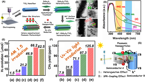
Plasmonic metal-based heterostructure nanofibers can be also obtained through controllably loading noble metal NPs onto electrospun semiconductor nanofibers by using chemical deposition or growth methods, such as atomic layer deposition, wet-chemical deposition, photodeposition, and hydro/solvothermal growth.[351-354] Recently, Zhang et al. found that the rational integration of LSPR of noble metal NPs with the heterojunction effect of semiconductors in the well-designed heterostructures can result in multi-channel improvement of kinetic behaviors of photogenerated charge carriers in the photocatalytic system. A successful example was achieved on the hetero-nanostructural plasmonic photocatalyst fabricated through hierarchical assembly of ultra-thin ZnIn2S4 NSs-intercalated plasmonic dimer-like metal (Au and Ag) NPs onto electrospun TiO2 nanofiber surfaces. The LSPR-coupling effect of plasmonic dimer-like structure can greatly boost the formation of photogenerated charge carriers in the photocatalyst by the PRET process. Meanwhile, the semiconductor heterojunction effect can further separate these charge carriers through the electrons transfer at ZnIn2S4/TiO2 interface. Thus, the Ag/ZnIn2S4/TiO2 photocatalyst with the optimal component and composition ratio exhibited about 11-fold enhancement on photocatalytic H2 production, and nearly 16-fold improvement on photocatalytic CO2 reduction as compared to the ZnIn2S4 NSs (Figure 18).[355]
4.2 Plasmonic Non-Metal-Based Heterostructures
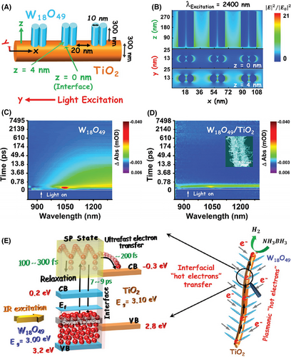
As compared to traditional plasmonic noble metal nanostructures, the burgeoning plasmonic nanostructures of non-stoichiometric semiconductors not only possess a cheaper price but also are more easily grown onto the surface of electrospun semiconductor nanofibers due to the low lattice mismatch between the two semiconductors. What’s more, plasmonic absorption bands of these semiconductor nanostructures often appear on IR light region, which offers an attractive opportunity to enable researchers to design and synthesize the IR-driven plasmonic photocatalysts by using the electrospinning technique. Zhang et al. have given a successful attempt to the solvothermal growth of plasmonic W18O49 NWs onto electrospun TiO2 nanofibers, forming nonmetallic W18O49/TiO2-branched heterostructures. Through ultra-fast transient absorption spectroscopy and finite-difference time-domain (FDTD) simulations, IR-driven transfer of plasmon-induced hot electron in the above branched heterostructures was demonstrated. The transfer of plasmonic hot electron from the W18O49 branches to the TiO2 backbones takes place within only ~200 fs in the branched heterostructure. This transfer process is much faster than the relaxation process (7–9 ps) of the hot electron from the surface plasmon state to the ground state in the W18O49 NWs. Thus, the W18O49/TiO2-branched heterostructure shows the enhanced photocatalytic H2 production from ammonia borane (NH3BH3) compared with that of W18O49 NWs under IR light irradiation to excite LSPR (Figure 19).[356] The comparison of photocatalytic activities for different electrospun plasmonic heterostructure photocatalysts are listed in Table 4.
| Photocatalyst | Plasmonic material | Mass | Incident light source | Conditions | Time | Activity | Refs |
|---|---|---|---|---|---|---|---|
| Au/CeO2 | Au | 1 mg | Vis/Xe lamp/λ > 420 nm | 100 μmol Benzyl alcohol in 2 mL acetonitrile under O2 atmosphere | 5 h | Benzaldehyde/392 μmol·g−1·h−1/selectivity of 100% | [ 346 ] |
| Simulated sunlight (UV-Vis)/Xe lamp | 5 h | Benzaldehyde/2360 μmol·g−1·h−1/selectivity of 100% | |||||
| Au/Pt/TiO2 | Au | 5 mg | UV-Vis/300 W/Xe lamp | L-ascorbic acid (aq)/10 mL/0.1 M/pH = 4 | -- | H2/11.658 μmol·h−1 | [ 347 ] |
| UV-Vis/500 W/Xe lamp | 90 mL gastight reactor bubbled with CO2 through deionized water | -- | CH4/0.57 μmol·h−1 | ||||
| Au/Pt/TiO2 | Au | 5 mg |
Dual-beam/300 W/Xe lamp/420 ± 10 nm +150 W/Xe lamp/550 ± 20 nm |
L-ascorbic acid (aq)/10 mL/0.1 M/pH = 4 | -- | H2/0.108 μmol·h−1 | [ 348 ] |
| Au/Ag/TiO2 | Au/Ag | 25 mg | Vis/40 W/LED daylight lamp | MB (aq)/50 mL/5 mg·L−1 | -- | RhB decomposition rate of 43 × 10−4/min | [ 354 ] |
| Ag/g-C3N4/TiO2 | Ag | 5 mg | AM 1.5/300 W/Xe lamp | TEOA (aq)/10 mL/15% | -- | H2/1.5 μmol·h−1 | [ 246 ] |
| Ag/ZnIn2S4/TiO2 | Ag | 5 mg | AM 1.5/300 W/Xe lamp | TEOA (aq)/10 mL/15% | -- | H2/33.1 μmol·h−1 | [ 355 ] |
| 5 mg | UV-Vis/300 W/Xe lamp/280–780 nm | 80 mL gastight reactor bubbled with high purity CO2 through deionized water | 4 h | CH4/~125.8 ppm | |||
| AgI-TiO2/PAN | Ag | 200 mg | Vis/300 W/Xe lamp/λ > 400 nm | MO (aq)/100 mL/5 mg·L−1 | 5 h | ~97% | [ 408 ] |
| Ag/BiFeO3 | Ag | 5 mg | Direct sunlight | MB (aq)/100 mL/10 mg·L−1 | 2 h | 100% | [ 353 ] |
| TiO2/WO3/Au | Au | 50 mg | UV-Vis/300 W/Xe lamp | Methyl alcohol (aq)/70 mL/~36% | -- | H2/269.63 μmol·h−1 | [ 291 ] |
| W18O49/TiO2 | W18O49 | 5 mg | IR/300 W/Xe lamp/λ > 750 nm | NH3BH3 (aq)/6 mL/~0.33 mg·mL−1 | -- | H2/0.22 μmol·min−1 | [ 356 ] |
| W18O49/C | W18O49 | 5 mg | IR/300 W/Xe lamp/λ > 750 nm | NH3BH3 (aq)/6 mL/~0.33 mg·mL−1 | -- | H2/0.14 μmol·min−1 | [ 388 ] |
5 Electrospun Flexible Self-Supporting Heterostructure Photocatalysts
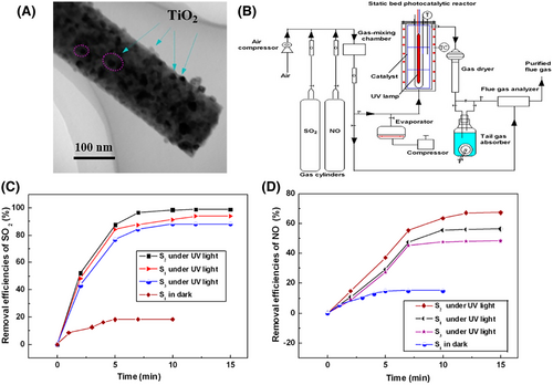
The electrospun flexible self-supporting nanofibrous membranes are mainly featured by the bendability, folding, twisting, compression, stretching, etc.[357] These advantages make the electrospun flexible self-supporting nanofibrous membranes as the ideal substrates to support the semiconductor nanostructured photocatalysts for the applications in the gas-phase and liquid-phase photocatalytic reactions.[358-360] Immobilization of semiconductor-based nanostructures onto the electrospun polymer nanofibers, such as polytetrafluoroethylene (PTFE), polyvinylidene fluoride (PVDF), polyamic acid (PAA), polymethyl methacrylate-co-methacrylic acid [P(MMA-co-MAA)], nylon 6,6, polyethersulfone (PES), and poly-L-lactide (PLLA), can achieve flexible self-supporting heterostructure photocatalysts.[361-367] This kind of photocatalysts inherits not only high photocatalytic activities of semiconductor-based nanostructures but also the properties of electrospun polymer nanofibrous membranes (e.g., flexibility, lightweight, self-supporting property, macroscopical processability, microcosmic porosity, and 3D open hierarchical structures). Owing to the hydrophobicity, and chemical and thermal stability, electrospun polyacrylonitrile (PAN) nanofibers have been frequently used as the supports for immobilizing the semiconductor-based nanostructures. Su et al. reported a novel photocatalysis system for simultaneous desulfurization and denitrification of flue gas over electrospun TiO2/PAN nanofiber photocatalysts. The flexible nanofibrous structure allows these photocatalysts to be easily assembled on the suitable position of the photoreactor for obtaining a larger gas flow rate and maximum utilization of the incident UV light. Furthermore, high microcosmic porosity of the electrospun membrane supporter leads to a very large gas–solid photoreaction interface during the photocatalytic reaction. Thus, this photocatalysis system can overcome some drawbacks of conventional gaseous pollutant removal systems (Figure 20).[358] Interestingly, Lee et al. give an attempt to extend the application of electrospun flexible self-supporting heterostructure photocatalysts in the area of sterilization. They found that ZnO NP-loaded PAN nanofibers possess a more effective photocatalytic bactericidal activity for Gram-negative E. coli and Gram-positive S. aureus under UV light irradiation than that of ZnO NPs. Also, after ten cycles, the kill percentages of these bacteria could still remain 96.6% over the ZnO/PAN composite nanofibers. These remarkable activities can be attributed to the unique 3D open hierarchical structures of the flexible nanofibers, thereby increasing its specific surface area.[368]
Constructing multi-functional semiconductor-based heterojunction units onto electrospun PAN nanofibers is a smart method to further improve the photocatalytic activities of the flexible self-supporting heterostructure photocatalysts. To date, many “type II” heterojunction systems, such as g-C3N4/BiOI, ZnO/TiO2, copper phthalocyanine/BiOCl, and ZnO/polyaniline, have been assembled onto electrospun PAN nanofibers for photocatalytic water purification.[230, 360, 369-371] Recently, Zhou and co-workers fabricated flexible g-C3N4/BiOI/PAN nanofiber photocatalysts via an in situ treatment of PAN/g-C3N4/Bi(NO3)3 composite nanofibers.[360] The strong chemical interaction between the g-C3N4 and BiOI heterocomponents leads to a highly effective separation of photogenerated charges across their “type II” heterojunction interface. What’s more, the flexible macroscopic network structures of these nanofibers photocatalysts enable them to float below the surface of the reaction solution for maximizing the absorption of the excitation light. Thus, the g-C3N4/BiOI/PAN nanofibers present high-efficiency photocatalytic activities for the decomposition of RhB and removal of toxic Cr(VI) ions upon visible light irradiation (Figure 21).[360] Based on the charge separation process of Ohmic or Schottky junctions, low-cost carbon-based nanomaterials, such as QDs, multi-wall NTs, and single-wall NTs, have been also employed to enhance the photocatalytic activities of UV or visible light-responsive semiconductor nanostructures supported on electrospun PAN nanofibers.[372, 373] Xie et al. prepared the novel flexible CQDs/Bi20TiO32/PAN core–shell structural nanofibers with the PAN as the core and CQDs/Bi20TiO32 composites as the shell using the coaxial electrospinning technique. The flexible carbon QDs/Bi20TiO32/PAN nanofibers showed both the excellent visible light-driven photocatalytic activity and the good recyclability for the decomposition of herbicide isoproturon.[374]

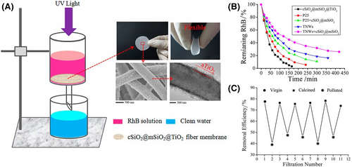
Besides the aforementioned polymer nanofibers, the electrospun SiO2-based composite nanofiber is another class of popular building block for constructing free-standing membranes with high flexibility and thermal stability. The flexible SiO2 nanofibrous membranes can be achieved through calcining the polymer template/SiO2 precursor composite nanofibers at a suitable calcine temperature (<1000 °C) due to the residual low-content carbonaceous species of polymer template in the formed amorphous SiO2 nanofibrous matrix to obstacle its embrittlement.[357, 375] Fortunately, the surface of the electrospun SiO2 nanofibers contains abundant active hydroxide groups, allowing the post-decoration of semiconductor or semiconductor-based photocatalysts with great convenience. Chen et al. have devoted much effort to the design and construction of flexible self-supporting heterostructure photocatalysts with electrospun SiO2-based nanofibers as the scaffolds for simultaneously optimizing the photocatalytic activity, mechanical strength, and thermal and chemical tolerance during the photocatalytic water purification. To increase the specific surface area, stability, and applicability, electrospun SiO2 nanofibers were clad by a mesoporous SiO2 shell layer through the modified Stöber method and subsequent calcination. Afterward, the obtained SiO2@mesoporous SiO2 core–shell nanofibers were muffled with the porous layer, which is composed of ultra-small anatase TiO2 nanostructures, through the hydrolysis of TiCl4 combined with the high-temperature calcination, thereby forming the unique core@double-shell structural nanofibers. This kind of composite fiber possesses several advantages for the photocatalysis application: 1) huge specific surface area; 2) high adsorbability on the pollutants; 3) high flexibility, excellent thermal stability, and easy to be compiled into the photocatalytic filtration membranes for widespread use; and 4) the all-inorganic components bringing great convenience in the remediation of photocatalysts from organic pollution via a simple calcination. Upon UV light irradiation, the SiO2@mesoporous SiO2-TiO2 core@double-shell nanofibers possess high photocatalytic activity for RhB decomposition as compared to that of commercial Degussa P25 (Figure 22).[376, 377] To further extend the light absorption region, the TiO2 component in the above SiO2 nanofiber-based flexible self-supporting photocatalysts has been replaced by the visible light-driven nanostructures, such as Bi2WO6 nanoplatelets, CuO NPs, Bi2WO6 NPs, and MIL-100(Fe), and g-C3N4.[378-382] These flexible nanofiber photocatalysts have high visible light photocatalytic activities, good tailorability, and excellent reusability for the application of photocatalytic organic pollutant decomposition. In addition, the flexible inorganic nanofibrous membranes have been also reported through the electrospinning preparation of the ion-doped TiO2, SiO2/TiO2, and carbon-based nanofiber systems under the suitable preparation conditions. These membranes can be also used as the flexible substrates to construct semiconductor-based free-standing heterostructure photocatalysts.[357] Thus, the design and fabrication of flexible self-supporting heterostructures through the electrospinning technique is a promising way for achieving high-performance membrane photocatalysts for practical photocatalytic application. In Table 5, we listed some typical examples of electrospun flexible self-supporting heterostructure photocatalysts for photocatalytic energy conversion and environmental remediation.
| Photocatalyst | Flexible substrates | Mass | Incident light source | Conditions | Time | Activity | Refs |
|---|---|---|---|---|---|---|---|
| PAN/BiOCl/BiOI | PAN | 20 mg | Full spectrum/300 W/Xe lamp/300 nm <λ < 2500 nm | RhB (aq)/100 mL/10 mg·L−1 | 1 h | 97% | [ 409 ] |
| PAN/Ag-AgBr@Bi20TiO32 | PAN | 100 mg | Vis/500 W/Xe lamp/λ > 400 nm | Isoproturon (aq)/50 mL/15 mg·L−1 | 54 h | 87.9% | [ 370 ] |
| ZnO/PAN | PAN | 500 mg·L−1 | UV/4 W/365 nm |
RB 5 (aq)/3 mg·L−1/pH = 6.67 or Rho B (aq)/3 mg·L−1/pH = 5.5 |
80 min | 100% | [ 368 ] |
| RB 5 (aq)/3 mg·L−1/pH = 6.67 | 2 h | CO2/0.243 mmol | |||||
| 10 mg | E. coli or S. aureus grown in LB media at 37 °C with continuous shaking at ~250 rpm with the cell suspension of ~1 × 10⁵ CFU·mL−1 | 25 min | 100% | ||||
| TiO2-PAN | PAN | 800 mg | UV/254 nm | SO2/1700 mg·m−3/200 mL·min−1/40 °C/humidity 5% | 15 min | 99.3% | [ 358 ] |
| NO/650 mg·m−3/200 mL·min−1/40 °C/humidity 5% | 71.2% | ||||||
| PAN-MWCNT/TiO2-NH2 | PAN | 15 mg | Vis/125 W/Xe lamp/λ > 400 nm | Ibuprofen/100 mL/5 mg·L−1/pH = 2 | 210 min | 100% | [ 410 ] |
| Naproxen/100 mL/5 mg·L−1 | 90 min | ||||||
| Cetirizine/100 mL/5 mg·L−1 | 50 min | ||||||
| ZnO@PVA/KGM | PVA | 2 × 2 cm2 | Solar simulator/300 W/Xe lamp/83 mW cm−2 | MO (aq)/100 mL/8 mg·L−1 | 2 h | 98% | [ 411 ] |
| PVDF-TiO2 | PVDF | 3.8 mg/45 cm2 | UV/six 4 W blacklight blue lamps/350–400 nm | BPA (aq)/45 mL/10 µM | 100 min | 100% | [ 367 ] |
| 4-CP (aq)/45 mL/10 µM | 1 h | 100% | |||||
| CMT (aq)/45 mL/10 µM | 2 h | 100% | |||||
| PI/ZnO | PI | 5 mg | UV/low-pressure Hg lamp | MB (aq)/5 mg·L−1 | 2.5 h | 98% | [ 412 ] |
| Pd@ZnO@Si@Nylon 6,6 | Nylon 6,6 | 1 × 1 cm2 | UV | MB (aq)/1.28 × 10−5 M | 1 h | 97% | [ 364 ] |
| ZnIn2S4/PVDF-poly(MMA-co-MAA) | poly(MMA-co-MAA) | 100 mg | Vis/500 W/Xe lamp/λ > 420 nm | MO (aq)/100 mL/10 ppm | 2 h | 92% | [ 363 ] |
| cSiO2@mSiO2@TiO2 | cSiO2@mSiO2 | 40 mg | UV/300 W/Osram Ultra-Vitalux UV light | RhB (aq)/100 mL/1.2 g·L−1 | 150 min | 95% | [ 376 ] |
| SiO2/MIL-100(Fe) | SiO2 | 5 mg | Vis/300 W/Xe lamp/λ > 400 nm |
RhB (aq)/20 mL/10 mg·L−1 + H2O2/10 μL |
70 min | 95% | [ 381 ] |
| TiO2/PES | PES | 0.5 cm × 0.5 cm/8–10 μm/~1.37 g·m−2 | UV/366 nm | MB (aq)/3 mL/1 × 10−5 M | 4 h | 20% | [ 365 ] |
| CNF@SnS2 | CNF | 50 mg | Vis/300 W/Xe lamp/λ > 400 nm | Cr(VI) (aq)/50 mL/250 mg·L−1/pH = 2 | 90 min | 100% | [ 271 ] |
| TiO2/carbon NFM | Carbon | -- | UV-Vis/300 W/Xe lamp | Loaded with the captured PM pollutant/0.1 mL of deionized water | 2 h |
CO2/53.0 ppm·h−1 CO/12.7 ppm·h−1; CH4/2.8 ppm·h−1 |
[ 266 ] |
| ZnO-poly-ʟ-Lactide | Poly-ʟ-Lactide | -- | UV/100 W/Hg lamp | MB (aq)/20 mL/5 ppm/5 mL·min−1 | 80 min | 90% | [ 366 ] |
| g-C3N4@NH2-MIL-88B(Fe)/bicomponent and multi-networked nanofibrous aerogels | Bicomponent and multi-networked nanofibrous aerogels | 25 mg | Simulated sunlight/500 W/Xe lamp |
Cr(VI) (aq)/50 mL/25 mg·L−1 +ammonium oxalate/10 mg +H2SO4/1 mmol·L−1/pH = 7 |
20 min | ~100% | [ 413 ] |
| 25 mg | Sulfamethoxazole (aq)/50 mL/20 mg·L−1/pH = 9 | 150 min | ~100% | ||||
| 100 mg |
TEOA (aq)/300 mL/10% +H2PtCl6/3 wt% (Pt nanoparticle) |
-- | H2/77.5 μmol·h−1 | ||||
| 50 mg | Salmonella typhimurium (TA98 and TA1535)/40 mL | 2 h | 79.8% and 76.4% |
6 Conclusiounsatisfactory because of the drawbacksns and Perspectives
Electrospinning technique provides a facile and universal approach for producing continuous ultra-long nanofibers of various semiconducting materials, including oxides, nitrides, and sulfides, and their composites. These electrospun semiconductor nanofibers with random arrangements are composed of tightly adherent nanoparticle units. As a consequence, the biscale porosity (the micron-sized pores at the gaps of interweaved nanofibers and the nanosized pores at nanoparticle units’ gaps), large ratio of surface to volume, ultra-high ratio of length to diameter, and abundant intercrystalline interfaces are well integrated within electrospun semiconductor nanofibers.[100, 117, 383] These unique structure properties are beneficial to improve the photocatalytic performance of traditional semiconductor photocatalysts toward energy conversion and environmental remediation, for example, photocatalytic reactants of whether liquid or gas can easily penetrate into porous structures of the electrospun nanofibers; amounts of intercrystalline interfaces in ultra-long 1D nanostructures can boost the migration and transport of photogenerated charge carriers on the surface of semiconductors. On the contrary, the multi-component semiconductor-based nanofibers with different heterostructures can be designed and fabricated through controlling the electrospinning parameters. In this way, many classical theories of solid state physics, that is, semiconductor-based heterojunction and surface plasmon resonance, have been purposefully introduced into the electrospun semiconductor-based nano-heterostructures for further improving both the light-harvesting ability and the photoinduced kinetic process of such charge carrier generation, separation, or migration. This review systematically summarizes recent advances on the design and electrospinning preparation of semiconductor-based nano-heterostructures for potential applications in photocatalytic water splitting/reduction and CO2 reduction, and photocatalytic decomposition of organic pollution from water or air. The highlights of this review focus on the discussions of how to engineer the photoinduced charge carrier kinetic through the rational assembly of photofunctional heterocomponents in/onto electrospun semiconductor nanofibers toward high-performance nano-heterostructure photocatalysts.
Although a large number of recent successful paradigms have been summarized to demonstrate the enhanced photocatalytic activities through synergistically optimizing the outside microstructures and the inner energy band configurations of electrospun nano-heterostructure photocatalysts, there are still many key issues that need to be answered for the purposes of both photocatalytic mechanism investigation and practical application. For achieving highly efficient photocatalytic solar-to-fuel conversion, the ideal photocatalyst should be characterized in broad-spectrum absorption, fast charge migration, and separated oxidation/reduction regions. In this regard, the controllable hierarchical synthesis of electrospun nano-heterostructures with well-integrated plasmonic nanostructures and semiconductor-based heterojunctions may be an exciting research direction. The selection of semiconductor heterojunction component/configuration, the moderation of plasmonic absorption band, and the elaborate construction of oxidation/reduction regions are three essential factors for influencing the photocatalytic activities of the obtained electrospun hierarchical nano-heterostructures. The electrospinning equipment should be continuously developed and updated so as to satisfy varied demands on the microtopography of the electrospun nanofibers. This will accelerate the pace of progress for realizing fine processing of photocatalytic oxidation and reduction regions or active sites on electrospun hierarchical nano-heterostructure photocatalysts that are synergistically sensitized by plasmonic nanostructures and semiconductor-based heterojunctions.
Electrospun flexible heterostructure photocatalysts have great potential for practical application in photocatalytic decomposition of organic pollution from water and air. However, the widely used flexible photocatalyst scaffolds are made by either polymer or SiO2-based nanofibrous materials, which inevitably induce some inconveniences during actual photocatalytic environmental remediation. It is essential to develop a new kind of electrospun flexible nanofibrous scaffold with excellent chemical and heat stability. Meanwhile, the immobilization process of semiconductor photocatalysts onto electrospun flexible nanofibrous scaffolds should be further investigated to avoid the separation between the photocatalysts and the scaffolds after a long-time photocatalysis. It is believed that the present review will arouse enough scientific interest in the electrospinning preparation of wide-spectrum-driven high-performance nano-heterostructure photocatalysts toward energy conversion and environmental remediation.
Acknowledgements
This work is supported by the National Natural Science Foundation of China (Grant Nos. 12074055 and 62005036), Liaoning BaiQianWan Talents Program, Dalian Science Foundation for Distinguished Young Scholars (2018RJ05), the Natural Science Foundation of Liaoning Province (Grant No. 2020-MZLH-15), and the Program for Dalian Excellent Talents (Grant No. 2020RQ131).
Conflict of Interest
The authors declare no conflict of interest.
Biographies

Na Lu received her PhD degree (2016) at Northeast Normal University and then initiated her independent career at School of Physics and Materials Engineering in Dalian Minzu University (2016). Her current research focuses on the design and synthesis of low-dimensional semiconductor-based materials for photocatalytic applications. She has published more than 30 SCI papers in the above fields such as Adv. Mater., Adv. Func. Mater., Appl. Catal. B- Environ.. Her current SCI H-index is 22 with over 1400 citations.

Mingyi Zhang is an associate professor of the School of Physics and Electronic Engineering at Harbin Normal University, PR China. He received his PhD degree (2013) at Northeast Normal University. His research interests focus on low-dimensional semiconductor-based materials for photocatalytic and electrocatalytic applications.

Peng Zhang received his Ph.D in Materials Physical and Chemistry from Northeast Normal University, China (2014). After postdoctoral research at Helmholtz-Zentrum Berlin, Germany, he joined the School of Materials Science and engineering at Zhengzhou University (2016). His current research interests focus on low dimensional carbon-based materials and their applications in the fields of environment remediation and energy storage. He has published more than 100 SCI papers in the above fields such as Adv. Mater., Adv. Func. Mater. His current SCI H-index is 37 with over 5000 citations including 11 ESI highly cited papers.

Zhenyi Zhang received his PhD degree in 2012 at Northeast Normal University and then worked as a postdoctoral research fellow at Solar Fuels Laboratory in Nanyang Technological University, before initiating his independent career at School of Physics and Materials Engineering in Dalian Minzu University in 2013. His current research focuses on the design and synthesis of low-dimensional semiconductor-based materials for photocatalysis and sensing applications. He has published more than 80 SCI papers in the above fields such as Adv. Mater., Adv. Func. Mater. His current SCI H-index is 45 with over 8000 citations including 11 ESI highly cited papers.


