Crystallization Regulation and Morphological Evolution for HTM-free Tin-Lead (1.28eV) Alloyed Perovskite Solar Cells
Abstract
There have been huge achievements of all-perovskite tandem solar cells, which recently realized the highest power conversion efficiency of 24.8%. However, the complex device structure and complicated manufacture processes severely restrict the further development of all-perovskite tandem solar cells. In this work, we successfully fabricated high-efficiency hole transport material-free (HTM-free) Sn−Pb alloyed narrow bandgap perovskite solar cells (PSCs) by introducing guanidinium thiocyanate (GASCN) and hydroiodic acid (HI) into the perovskite precursor solution. GASCN and HI play a positive synergy effect during perovskite crystallization process resulting in larger grain size, fewer surface defects, and lower trap density to suppress the Sn2+ oxidation degradation. Furthermore, they could effectively adjust the energy level of perovskite materials, reduce the energy level difference between perovskite and ITO resulting in more efficiently transport of free hole charge carriers. As a result, with adding GASCN and HI, the achieved highest power conversion efficiency of HTM-free devices increased from 12.58% to 17.85%, which is one of the highest PCEs among all values reported to date for the HTM-free narrow-bandgap (1.2–1.4 eV) Sn−Pb binary PSCs. Moreover, the optimized device shows improved environmental stability. Our additive strategy manifests a remarkable step towards the facile, cost-efficient fabrication of HTM-free perovskite-based tandem solar cells with both high efficiency and simple fabrication process.
1 Introduction
In the last decade, there are enormous remarkable progresses in organic–inorganic hybrid perovskite solar cells (PSCs) have been achieved. Up to now, the certified highest photoelectric conversion efficiency (PCE) of single-junction lead halide PSCs has reached 25.5%,[1] which is comparable to traditional crystalline silicon cells, CIGS (copper indium gallium selenide), and GaAs (gallium arsenide) solar cells. Recently, in order to obtain even higher energy harvesting efficiency, an increasing number of researches are focusing on perovskite/Si,[2-4] perovskite/CIGS,[5-7] and monolithic all-perovskite tandem solar cells, which shows great promise for ultrahigh efficiency (>40%).[8-10] Among these tandem solar cells, the all-perovskite tandem solar cell shows great potential as an ideal candidate to surmount the Shockley-Queisser limits on account of the low-temperature processability and tunable bandgap.[11-14]
The two terminal monolithic all-perovskite tandem devices usually consist of a narrow-bandgap (NBG; 1.1–1.3 eV) bottom subcell and a wide-bandgap (WBG) (1.7–1.9 eV) top subcell.[13, 15, 16] The classical device architecture of all-perovskite tandem solar cells is glass substrate/ITO (indium tin oxide)/HTL (hole transport layer)/WBG-perovskite/ETL (electron transport layer)/SnO2 (tin dioxide)/ITO/HTL/NBG-perovskite/ETL/BCP (bathocuproine)/metal electrode,[10, 17] which is very complicated. The masses of functional layers basically mean various processing techniques and high cost that could gravely limits its promising future prospects.[18, 19] Even more, these high-temperature sputtering process and solution preparation methods might cause damage to underlying functional layers. For example, the preparation of PEDOT:PSS aqueous solution as HTL of bottom subcell may damage the underlying layers and the hydrophilic PEDOT:PSS also seriously shorten the long-term stability of PSCs due to its poor thermal stability.[20, 21] The charge carrier transporting and recombination efficiencies between functional layers also play a critical role in determining device performance, which means the poor interfacial contact might lead to more interfacial trap recombination.[22-24] Liao et al. fabricated HTM-free PSCs based on FAPb0.5Sn0.5I3 and realized 7.94% PCE in 2017.[25] In 2019, McGehee et al. successfully prepared Sn–Pb mixed NBG cell without HTM with PCE of 16.4% and close to 21% for all-perovskite tandem devices.[20] Huang et al. designed an advanced simple interconnection layer between two subcells and achieved a high PCE of 24.4% with great long-term stability.[18]
As for Sn–Pb mixed narrow bandgap bottom subcells, the poor performance and instability problem were mainly caused by the oxidation of Sn2+ located at the surface defects and grain boundaries.[26, 27] During the oxidation process, the increasing defects density resulted from Sn4+ limits the charge carrier transporting and carrier lifetime. Therefore, applying effective dopants and surface passivation techniques to decrease the defects density of Sn–Pb mixed perovskites was a key method to enhance the device performance. Recently, there are some small additives have been employed to reduce the trap density in Sn–Pb mixed perovskites, such as Tin difluoride (SnF2[28]), Sn powder,[26] GABr,[29] PHCl,[30] and much more.[31]
Herein, we established an effective method to successfully fabricate high performance HTM-free narrow bandgap PSCs, which possesses a promising prospect on all-perovskite tandem solar cells. Moderate HI and GASCN were cooperatively introduced into the perovskite precursor solution to adjust the dynamic nucleation procedure aiming to effectively improve crystalline quality. By reducing phase segregation and enlarging grain size to form compact perovskite surface, the Sn–Pb mixed perovskite films successfully have much less oxidation of Sn2+ to Sn4+ at grain boundaries and surface defects. Furthermore, the HI and GASCN could effectively adjust the energy level of perovskite materials, reduce the energy level difference between perovskite and ITO resulting in more efficient transport of free hole charge carriers. As a result, compared to 12.58% for control devices, the best PCE of 17.85% was achieved in the HTM-free NBG (1.28 eV) PSCs, which is the highest PCEs among all values reported to date for the HTM-free NBG (1.2–1.4 eV) Sn−Pb binary PSCs. Moreover, the optimized device shows improved environmental stability with <20% loss of its initial efficiency after being tested in high humid environment (60%–80% RH) and then stored in glovebox for about 240 h. Our additive strategy proposes a new way to fabricate HTM-free perovskite-based tandem solar cells. This work manifests a remarkable step towards the facile, cost-efficient fabrication of PSCs with both high efficiency and simple fabrication process.
2 Results and Discussion
In this work, we fabricated HTM-free PSC devices with directly depositing (FAPbI3)0.7(MASnI3)0.3 perovskite layer on bare ITO substrates with PC61BM as electron transport layer and BCP on the perovskite as shown in Figure 1a. Figure S1 (Supporting Information) showed the performance of HTM-free and PEDOT-based control devices. For the HTM-free devices, we achieved the best device with stabilized PCE of 12.58% despite the open circuit voltage (Voc) was only 0.67 V and the short circuit current density (Jsc) was 26.81 mA cm−2, which were both little smaller than PEDOT-based devices due to the lack of hole extraction layer. The present results indicated the actionability and enormous potential for fabricating HTM-free narrow bandgap Sn−Pb mixed PSCs and even being transferred to monolithic all-perovskite tandem solar cells.[20, 25]
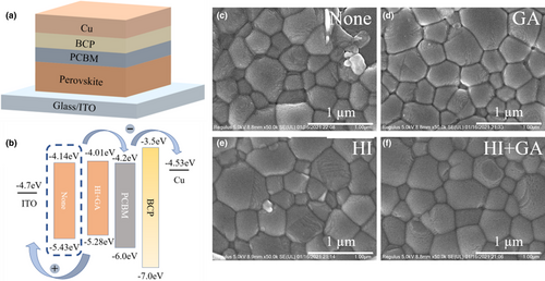
Although we successfully prepared HTM-free Sn−Pb mixed PSCs, the devices performance obviously was not good enough to transfer into all-perovskite tandem solar cells. The poor performance was mainly caused by the oxidation of Sn2+ located at the surface defects and grain boundaries.[27, 32] Therefore, in order to achieve better HTM-free NBG PSCs, HI solution and GASCN were carried out in this work and their synergistic effect in fabrication process was observed. The (FAPbI3)0.7(MASnI3)0.3 perovskite layer was prepared as details shown in the experimental section and their surface morphologies were characterized as indicated in Figure 1c–f and Figure S2 (Supporting Information). In order to directly view the perovskite crystal size, the grain size distributions were summarized and plotted as in the frequency chart (Figures S3 and S4 in the Supporting Information). For the obtained pristine perovskite layer (Figure 1c), there were lots of small grains, surface pinholes, and impurity phase at the grain boundaries, which all could cause severe nonradiative recombination. Also, from the atomic force microscopy (AFM; Figure S2 Supporting Information), the average surface roughness of the unadded perovskite was high to 26.3 nm. For the GASCN-added perovskite layer (Figure 1d), the surface morphology was obviously improved and the grains were more uniform when comparing to pristine devices. GASCN adding into perovskite precursor solution could play a positive role in increasing perovskite grain size and improving film morphology due to SCN ions.[33, 34] Besides, From Figure S5 (Supporting Information), there was obvious shift of the characteristic peak, which could mean the existence of GA left in the perovskite film. GA cations located at grain boundaries could form a stable two dimensional (2D) structure, which could improve photovoltaic properties substantially.[29, 33, 35-37] The 2D structure not only could effectively reduce oxygen in the air diffusing into perovskite layer through grain boundaries to suppress the oxidation of Sn2+, but also could block the diffusion of ions through grains to form excessive vacancies. In addition, there was also significantly enhancement in perovskite morphology as shown in Figure 1e when only adding HI into the perovskite precursor solution. It is found that HI could react with Lead diiodide (PbI2) to form an intermediate, hydrogen lead iodide (HPbI3+x) in the perovskite precursor solution.[38-41] As we know, tin-based perovskite has much faster nucleation speed than lead-based perovskite, which means the difference of crystallization rate would easily cause serious phase separation during the annealing process.[42] Therefore, the formation of HPbI3+x or HSnI3+x intermediates could effectively slow down the crystallization process involving the cations exchange of H+ and MA+/FA+ in the framework.[38] With both adding GASCN and HI into the perovskite solution, there were more compact and uniform perovskite grains achieved in Figure 1f and the average surface roughness of ideal perovskite layer was only 18.9 nm due to the synergistic effect of GASCN and HI. Figure 1b and Figure S6 (Supporting Information) showed the energy diagram of the pristine, GASCN and HI-added device, which is extracted from the UV-photoelectron spectroscopy (UPS) characterization spectra in Figures S7 and S8 (Supporting Information) and the ultraviolet–visible (UV–vis) absorption spectra in Figure 2b. Adding GASCN and HI could effectively adjust the energy level of perovskite materials. There was slightly increase of the Highest Occupied Molecular Orbital of perovskite material with adding GASCN and HI, resulting in more efficient transport of free hole charge carriers.
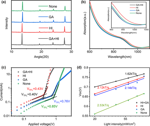
In order to further explore the effect of GASCN and HI on perovskite crystallinity, Figure 2a depicted the X-ray diffraction (XRD) patterns of GASCN and HI-added, GASCN-added, HI-added, pristine perovskite films deposited on ITO substrates, respectively. From the XRD results, it was obviously observed that there were stronger and sharper (110) and (220) lattice planes at around 14° and 28° of the perovskite film with introducing GASCN and HI than the pristine perovskite, which indicated that the perovskite with GASCN and HI contained higher phase purity and well-oriented crystal structure. To further verify the existence of the intermediate phase, the XRD characterization was carried out to measure the pristine and annealed perovskite films while adding HI solution. As shown in Figure S9 (Supporting Information), there was obvious characteristic peak at around 11.5° for HPbIx before annealing and vanished after annealing for 10 min at 100 °C. This is consistent with many previous literature reports.[38, 40] Figure S10 (Supporting Information) also demonstrates the absence of the DMAPbI3 intermediate in the perovskite film while adding HI solution.[41] Figure 2b and Figure S11 (Supporting Information) showed the UV–vis absorption spectra of the above perovskite films. The GASCN-added perovskite film contained the smallest light absorption cutoff value, which was 960 nm and on the contrast, the largest cutoff value was improved to 978 nm with only adding HI into perovskite precursor solution; 964 and 968 nm were, respectively, the cutoff values of pristine, both GASCN and HI-added perovskite materials. In other words, the bandgap of perovskite materials decreased to 1.28 eV from 1.29 eV when adding HI and GASCN. Furthermore, there was obvious enhancement of absorption intensity after adding HI into perovskite, which might be due to the improvement of perovskite morphology. From the absorption graph, HI played the most important role in lowering the bandgap and strengthening the absorption intensity of perovskite material.[38, 43]
Figure 2d showed the light intensity dependent Voc of the four kinds of PSCs. These devices, respectively, exhibited slopes of 1.62, 2.12, 2.14, and 2.53 kT q−1 for both HI and GASCN added, HI-added, GASCN-added and pristine PSCs. The slope derived from (kT q−1) was closely related to trap-assisted recombination in perovskite film that the smaller slope value suggested the smaller energy loss from trap-assisted recombination.[47, 48] As a result, it was obvious to infer that HI and GASCN could both effectively reduce surface defects and trap density and finally lead to higher Voc and Jsc of PSCs. The device added by both GASCN and HI contained the lowest slope of 1.62 kT q−1, which was consistent with the best device performance. The photoluminescence (PL) spectra of the corresponding perovskite films were also provided as shown in Figure S12 and Table S1 (Supporting Information) to support the result from SCLC characterization. The PL emission peak intensity of the perovskite films was apparently increased sequentially from pristine, GASCN-added, HI-added, both GASCN and HI-added perovskite films, which meant the positive effect of GASCN and HI in the suppression of non-radiative trap-assisted recombination.
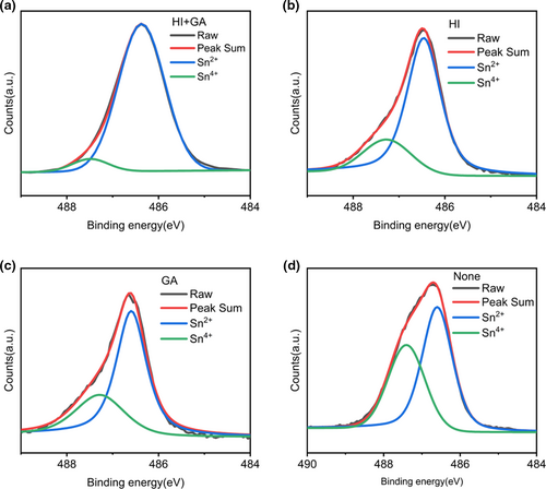
In order to further explore the effect of GASCN and HI on the suppression of high-density defects induced by Sn2+ oxidation in Pb-Sn perovskite film, Sn elements in various perovskite materials were detected using X-ray photoemission spectroscopy (XPS). Figure 3a–d conveyed the XPS spectra of Sn 3d core-level of GASCN and HI-added, HI-added, GASCN-added, and pristine perovskite films respectively. By deconvoluting each spectrum with Sn2+ (486.8eV) and Sn4+ (487.5 eV) peaks, the amount of Sn4+ at the surface were calculated.[49, 50] From Figure 3d, the ratio of Sn4+ was 41.5% without adding GASCN or HI. The amounts of Sn4+ decreased to 31.6% and 21.1% when adding GASCN and HI respectively as shown in Figure 3b,c. As for both adding HI and GASCN in perovskite precursor solution, the ratio of Sn4+ lowered to only 6.3% in Figure 3a. As a consequence, introducing GASCN and HI into perovskite precursor solution could effectively suppress the oxidation of Sn2+.
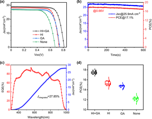
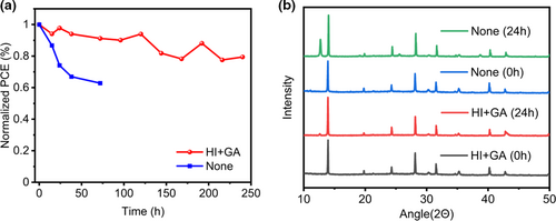
The PSCs with a structure of ITO/Perovskite/[6,6]-Phenyl C61 butyric acid methyl ester (PCBM)/BCP/Cu were fabricated to observe the cell performance under AM 1.5G solar 100 mW cm−2 simulator illumination. Figure S13 and Table S2, Figure S14 and Table S3 (Supporting Information) provide an optimized concentration of HI solution and GASCN, respectively. Figure 4a indicated the cell performance of HTM-free PSCs with different adding conditions and their particular parameters were summarized in Table 1. Pristine (FAPbI3)0.7(MASnI3)0.3 device showed the worst cell performance in PCE of 12.58% with a Jsc of 26.81 mA cm−2, a Voc of 0.67 V and an FF of 73.79%. While adding GASCN or HI respectively into perovskite precursor solution, there were effective increase of PCEs. For the only GASCN adding, the best device achieved a PCE of 14.95% with a Jsc of 27.03 mA cm−2, a Voc of 0.75 V and an FF of 74.19%. On the contrast, as for only HI adding device, the best resulted PCE was 15.82% with a Jsc of 28.24 mA cm−2, a Voc of 0.74 V and an FF of 76.16%. For the cell under the synergistic effect of GASCN and HI, we realized the highest PCE of 17.85%, which was 40% higher than the pristine device, with a Jsc of 28.94 mA cm−2, a Voc of 0.81 V and an FF of 75.90%. Figure S15 (Supporting Information) showed the forward and reverse scanning efficiency of the champion device with the scan rate of 0.02 V/step and the delay time of 0.001 ms. Comparing to previous report on the Sn−Pb alloyed narrow bandgap HTM-free PSCs, the best cell we prepared in this work has the highest PCE (see Table S4, Supporting Information). Figure 4c gave the external quantum efficiency (EQE) spectrum of both GASCN and HI added best device. The improved EQE was inspected in the range of 300–980 nm, which was consistent with the band edge of the previous UV–vis absorption spectra and PL emission peaks. The integrated photocurrent density from the EQE spectra of GASCN and HI both added (FAPbI3)0.7(MASnI3)0.3 device was 27.85 mA cm−2, which was consistent with the Jsc value in J-V measurement. Figure 4b showed the steady-state measurement for Jsc and PCE at the maximum power point (MPP) for the best device added by GASCN and HI. The inspected Jsc and PCE of both GASCN and HI added (FAPbI3)0.7(MASnI3)0.3 device, respectively, stabilized at around 25.9 mA cm−2 and 17.1%. Figure 4d showed the average efficiency of the four devices. As for the long-term stability measurement, the prepared PSCs without encapsulation were measured under humid (RH >70%) environment and then transferred into glovebox to store. The PCE of pristine PSCs dropped quickly under 60% of its initial value after stored for only 72 h as shown in Figure 5a. On the contrast, with adding both GASCN and HI into perovskite precursor solution, the stability of PSCs could be substantially enhanced with a decrease of 20% after 240 h. Besides, Figure 5b also suggested the change of XRD patterns for pristine and both HI and GASCN-added perovskite materials while being exposed under air environment for 24 h. For the pristine perovskite film, there was obvious degradation of perovskite material due to the high diffraction intensity of PbI2 characteristic peaks after reacting with oxygen and water in air. On the contrary, there was not much difference in XRD patterns for GASCN and HI-added perovskite material and only a small amount of PbI2 was produced. As a result, introducing GASCN and HI could efficiently enhance the long-term stability of perovskite material.
| PCE [%] | Jsc [mA cm−2] | Voc [V] | FF [%] | |
|---|---|---|---|---|
| HI+GA | 17.85 | 28.94 | 0.81 | 75.90 |
| HI | 15.82 | 28.24 | 0.74 | 76.16 |
| GASCN | 14.95 | 27.03 | 0.75 | 74.19 |
| Pristine | 12.58 | 26.81 | 0.67 | 73.79 |
3 Conclusion
In summary, an effective and novel strategy in this work has been demonstrated by introducing both HI and GASCN into Sn−Pb alloyed perovskite precursor solution to successfully prepare high-efficiency HTM-free narrow bandgap PSCs. HI and GASCN both play a positive synergistic effect during crystallization process resulting in larger grain size, more compact morphology and much fewer surface defects in perovskite film. Furthermore, they could effectively adjust the energy level of perovskite materials, reduce the energy level difference between perovskite and ITO, resulting in more efficient transport of free hole charge carriers. After respectively adding GASCN and HI into perovskite solution, the highest PCEs of PSCs respectively increase to 14.95% and 15.82% from only 12.58%. Furthermore, the achieved highest PCE of both GASCN and HI-added perovskite precursor solution is up to 17.85%. Besides, for GASCN and HI-added PSCs, there is <20% loss of its initial efficiency after being tested under hazard environment (60%–80% RH) and then stored in glovebox for about 240 h. This work introduces a remarkable path to fabricate efficient and stable Sn−Pb alloyed HTM-free narrow bandgap PSCs. This kind of narrow bandgap PSCs in simple structure can be believed and attached importance to fabricate monolithic all-perovskite tandem solar cells.
4 Experimental Section
Materials
Tin diiodide (SnI2, 99.99%) was purchased from Advanced Election Technology Co., Ltd. PbI2 (99.99%), PCBM (99%) and 2, 9-Dimethyl-4, 7diphenyl-1, 10-phenanthroline (BCP, 99%) were obtained from Xi’an Polymer Light Technology. SnF2 (99%) and GASCN (99%) was obtained from Aladdin Industrial Corporation. Methylamine iodide (MAI, 99.99%) and Formamidinium iodide (FAI, 99.99%) were obtained from Greatcell Solar Materials Pty Ltd. Hydroiodic acid (HI, 57%), N, N-dimethylformamide (DMF, 99.8%), dimethyl sulfoxide (DMSO, 99.8%), isopropyl alcohol (IPA, 99.8%), chlorobenzene (99.8%) as well as toluene (99.8%) were acquired from Sigma-Aldrich Company. All the chemicals and solvents were received and applied without further purification.
Fabrication of PSC devices
The perovskite precursor solution was prepared by mixing FAI, MAI, PbI2, and SnI2 powders with molar ratio as 1.5 m (FAPbI3)0.7(MASnI3)0.3; 10% SnF2 in molar ratio to SnI2 was added. For each milliliter precursor solution, 5 mg GASCN was added. The ideal solvent was obtained by mixing 800 μL DMF and 200 μL DMSO. After dissolving completely, 10 μL HI solution was added into precursor solution. Patterned ITO coated glass substrates were sequentially cleaned by ultrasonic cleaner for 15 min in detergent, DI water, acetone, and isopropanol. The substrates were then dried by nitrogen flow and were put into ultraviolet-ozone chamber for 15 min. After UVO treatment, the substrates were transported into nitrogen-filled glovebox to fabricate perovskite layer. After being filtered by 0.22 μm PTFE filter, 80 μL perovskite precursor solution was dripped on the substrates. For this one-step solution casting process, the spinning speed was 4000 rpm for 30 s and 150 μL toluene was dropped onto the center of spinning substrates at 5 s before the end. Afterwards, the casted substrates were shifted on 100 °C hot plate to anneal for 10 min. After cooling down to room temperature, 20 mg mL−1 PC61BM dissolved in chlorobenzene was coated on perovskite layer at 1000 rpm for 60 s. Lastly, 8nm BCP and 100 nm metal silver electrode were sequentially thermal evaporated in vacuum chamber at pressure <4 × 10⁻⁴ Pa through a shadow mask with active area of 0.1 cm2.
Characterization
The J-V measurement of the devices without encapsulation was carried out in air (60%–70% humidity) at room temperature using a shadow mask by a computer controlled Keithley 2400 Source Measure Unit under AM1.5G solar 100 mW cm−2 simulator illumination (Enlitech Solar Simulator SS-F7-3A). The light intensity was calibrated by a standard silicon solar cell. The EQE was performed using a DSR100UV-B spectrometer with an SR830 lock-in amplifier. The steady-state PCE was measured by recording the value of the photocurrent density at the largest power output bias voltage. The XRD patterns were obtained by using the Bruker ECO D8 (Bruker, Germany) system. The UV–vis absorption spectra of the perovskite films were obtained by using the spectrophotometer (Perkin Elmer Lambda 750). Scanning electron microscopy (SEM) images were obtained by using the field-emission SEM (FEI Nova_Nano SEM 430). AFM images were obtained by the Bruker Dimension Icon in the Tapping mode. PL and time-resolved photoluminescence (TR-PL) were measured with Edinburgh Instrument FLS980. XPS spectra were carried out by ThermoFisher Nexsa and UPS was measured with ThermoFisher Escalab 250Xi.
Acknowledgements
H.H. and X.Z. contributed equally to this work. This work was financially supported by the Joint Funds Project funding from Guangdong Basic and Applied Basic Research Foundation (Grant No. 2019B1515120083), the National Natural Science Foundation of China (Grant No. U19A2089), the Key Fundamental Research Project funding from the Shenzhen Science and Technology Innovation Committee (Grant No. JCYJ20200109141014474), the National Key Research and Development Project from the Ministry of Science and Technology of China (Grants Nos. 2016YFA0202400 and 2016YFA0202404), the Peacock Team Project from Shenzhen Science and Technology Innovation Committee (Grant No. KQTD2015033110182370), Shenzhen Engineering R&D Center for Flexible Solar Cells project funding from Shenzhen Development and Reform Committee (Grant No. 2019-126), and the Guangdong-Hong Kong-Macao Joint Laboratory (Grant No. 2019B121205001).
Conflict of Interests
The authors declare no competing interests.


