Negative differential conductance materials for flexible electronics
ABSTRACT
The need for electronics that is compatible with life is driving the search for electronically active materials that may be used for transferring integrated circuits onto flexible substrates. One route is to build transistors, which modulate the conductivity of organic thin films with a lateral gate. However, as is well known in the case of graphene, the in-plane conductivity cannot easily be switched off. Another route is to use negative differential resistance (NDR) phenomena. Until recently, NDR was only obtained from band engineered semiconductors. This article reviews the recent development of flexible materials that specifically make use of transport perpendicular to graphite planes to obtain NDR. These materials include h-boron-nitride/graphene multilayers and graphite-silicone composites. We report on the dependence of their current-voltage curves on deformation, changes in structural and experimental parameters. We also describe device implementations in the form of flexible oscillators, amplifiers and memories. © 2013 Wiley Periodicals, Inc. J. Appl. Polym. Sci. 2014, 131, 40169.
INTRODUCTION
Background
For decades, the miniaturization of transistor circuitry has underpinned progress in electronics. Increases in integration density have brought gains in speed and memory capacity while dramatically reducing power consumption. The latter has dropped by 4 orders of magnitude from 0.4 μJ per floating point operation (flop) in 1997 to 70 pJ in 2012. Although the scaling down of integrated circuits has been predicted to reach its physical limits for many years, technological prowess, notably the development of high permittivity dielectrics, has enabled the scaling of transistor gates to dimensions as small as 22 nm. Over the next decade, energy requirements are forecast to drop to 5–10 pJ per flop. In parallel with the miniaturization in silicon chips, novel materials have been sought to build integrated circuits on flexible substrates.1, 2 This effort is motivated by the need for ergonomic human-computer interfaces that fit the human body, curved surfaces, and moving parts. Applications areas include conformable displays,3-8 touch sensitive pads,9-13 Braille displays,14 body wearable sensors,15, 16 medical probes and implants,17-19 artificial retinas,20, 21 and artificial skins.22, 19, 23-25 As most flexible materials are electrical insulators, attention has focused on conjugated polymers that allow electrons to delocalize along molecular chains and hop from one molecule to another. These polymers tend to have p-type conduction,26 which hinders the realization of CMOS logic. Recently electric field induced ambipolar conduction has also been achieved.27, 28 Organic polymers are prone to decay under bias voltage cycling and oxidation at the site of the conjugated bonds. The development of organic thin films for transistors,26, 28 molecular electronics,29 and organic electro-luminescent devices has already been covered in excellent reviews.29-31
Aims
The purpose of this review is to report on novel graphitic compounds that exhibit negative differential resistance (NDR) in their current-voltage (I–V) curves. These materials combine electronically active properties with the ability to bend. The NDR is a region of the I-V curves where the current decreases (
 ) when the bias voltage increases (
 ). The negative differential conductance
 is the figure of merit that defines active properties such as the voltage and power gain.32 Here, we describe the synthesis of these materials and the physical mechanisms underpinning the NDR as these differ from quantum mechanical tunneling in band engineered semiconductors. We show how NDR devices achieve the traditional functions of transistors such as voltage amplification,32 bistable memories and are unique in implementing multilevel logic,33 and high frequency generation.34, 35 The recent demonstration of NDR in flexible materials opens an exciting new direction for fundamental research on the coupling between mechanical deformation and electronic gain, which opens a range of new possibilities for electromechanical sensing.36, 37
Table 1 shows the main families of devices fabricated on rigid and flexible substrates. Field effect transistors and optoelectronic devices have already been translated from silicon or III–V semiconductors to organic thin films. In contrast, NDR devices such as Esaki diodes, double barrier resonant tunneling structures and superlattices have only been implemented on crystalline substrates. These devices require band engineered semiconductor structures, which are modulated on the atomic scale and are defect free to produce a tunneling current, which decreases with increasing voltage. These are stringent conditions for organic thin films, which are not easily structured at the supramolecular level. This article reports on the observation of tunneling NDR in flexible graphitic compounds, which combine long range atomic order with flexibility. These are the graphene-boron nitride38 and graphite-silicone39 systems in which a current may be injected perpendicular to the atomically thin graphite planes.
| Transistors | NDR Devices | Optoelectronics | |
|---|---|---|---|
| Rigid substrates | Field effect transistors | Esaki diodes | Light Emitting Diodes |
| Bipolar transistors | Semiconductor superlattices | Optocouplers, | |
| Resonant tunneling diodes | LASER heterojunctions | ||
| Flexible substrates | Organic transistors | →This review← | Organic electroluminescent devices |
A New Dawn for NDR Devices?
From a technological stand point, one may ask what benefit would the novel graphitic structures confer to NDR devices given that semiconductor NDR has only so far supplanted transistors in niche application such as high frequency mixing.35 In fact, perpendicular transport through graphene planes presents many advantages over semiconductor multilayers. In III–V tunneling structures, quantum resonances, and the associated NDR have been blurred by the thermionic current component activated over the tunneling barriers. These problems have been addressed by using materials with higher tunneling barriers such as boron nitride,38 or polysilane39 to quench the thermionic current. Second, the tunneling process leading to NDR in graphitic compound is very robust, as it does not involve resonance through a localized energy level bound to quantum well. Further, the peak-to-valley current ratio, which measures the switching contrast - can theoretically be infinite39 unlike in semiconductor multilayers. Third, the graphene-boron nitride tunneling system has both atomically thin graphene electrodes and boron-nitride barriers which allows atomic level miniaturization.38 Fourth, graphene boron-nitride trilayers have negligible transit times due to the absence of a central quantum well. As a result, one expects faster response time than in resonant tunneling structures where Fabry-Perot type resonances impose a dwell time of a few picoseconds. Boron-nitride trilayers could thus operate as quasi-optical sources at generating frequencies in excess of the THz. Fifth, the flexibility of graphitic materials has allowed the voltage oscillations generated by the NDR region to be tuned by strain. In this way, the NDR material mimics the response of biological mechanoreceptors and opens a new route towards accurate pressure sensing. The conversion of strain into voltage oscillations of frequency proportional to strain replicates the response of electromechanical sensors (Merkel cells)40, 41 in the skin. The coding of strain into frequency is believed to explain the high sensitivity of the human touch.
Perpendicular transport presents an attractive alternative to in-plane transport in graphene as the lack of energy band gap makes it difficult to turn off the in-plane conduction through the action on an electrostatic gate. By contrast, perpendicular transport in graphitic compounds has already obtained amplification gain, electromechanical sensing, and offers high peak-to-valley current ratios with the real prospects of material improvement in the near future.
Organization of the Article
The article is organized as follows. Section “Introduction” presents the background and motivations; Section “ Flexible Electronics” reviews the science and technology of transistors and electro-luminescent devices made from flexible materials as well as the routes towards their synthesis; Section “Materials for Negative Differential Resistance” covers the materials for NDR including semiconductors, metal-organic thin films, graphene-boron-nitride trilayers, and graphite-silicone composites; Section “Electromechanical Response of Strained NDR Devices” describes the behavior of the NDR under strain and the analogy with mechanoreceptors in the human skin; Section “Applications of Flexible NDR” describes demonstrates voltage amplification by plastic materials and proposes simple multilevel memories; the conclusion summarizes the advantages and drawbacks of graphitic NDR materials and identifies future challenges.
FLEXIBLE ELECTRONICS
Flexible circuits require specific materials for interconnects, logic gates, power storage cells, sensing, and actuation. Circuit flexibility is generally gauged by the ability to operate at tight bend radii. Organic thin films have lower electron mobility and optical quantum efficiency than semiconductors; however, their low fabrication costs and printability have made them a good choice for large area displays, sensor arrays, and bioelectronics. Current research efforts on organic materials are directed toward increasing the resistance of conjugated polymers to oxidation, which is known to degrade mobility over time.26 Increasing the resilience to bias voltage cycling and mechanical fatigue are also important research areas to improve material performance.28, 42 Shape memory is another factor, which limits the electromechanical response time to between 10 ms and several minutes.23
An alternative route pioneered by John Rogers's group at the University of Illinois1 is to micromachine semiconductor membranes on elastomeric substrates using the island-bridge approach. The islands are semiconductor devices transferred from a crystalline substrate onto a flexible substrate using lift-off techniques. Individual islands are then bridged by nanoribbons carefully engineered to obtain a flexible semiconducting mesh. Although this approach does not quite achieve the level of flexibility of organic films, it allows high performance semiconductor devices including fast transistors, multicolor light emitting diodes, temperature sensors, etc. to be integrated on flexible platforms. This has opened important new possibilities for medical research for instance in optogenetics.43
Flexible active devices have also been made from composite thin films. These materials typically incorporate conductive nanoparticles (usually carbon) in an insulating elastomer.44 This route has been very successful in making addressable arrays of conformable pressure sensors and actuators.6, 9, 45, 46 Generally soft conducting composites give an order of magnitude larger electromechanical coupling than silicon or GaAs, the latter's piezoresistance being 1.1% per atmosphere.47
Before reviewing the three classes of materials above, it is useful to examine the physical requirements that pressure sensors must meet to solve modern technological challenges. To our knowledge, the most stringent conditions are set by the need to image turbulent flow.48 Currently, the best pressure and shear stress sensors are micromachined in-silico. They have dimensions of 100 microns and sensitivity of 50–500 kPa, which is inadequate.22 Imaging turbulence in the air boundary layer of an aircraft is an outstanding challenge,48 which calls for sensor arrays sampling pressure changes at a rate of 1 kHz, with sensitivity of at least 1 kPa, and spatial resolution better than 26 μm.
Organic Transistors
Organic transistors are synthesized from either small conjugated molecules such as pentacene or conjugated polymers such as polythiophene or PEDOT.26, 42 The former are prepared by thermal sublimation and have been used to make addressable arrays of organic transistors with excellent flexibility.28, 45 The latter by contrast have better resistance to oxidation and higher mobility up to 0.1 cm2 V−1 s−1. Polymer films were obtained by inkjet printing,49, 50 paper-like inline printing,51, 52 subtractive lift-off lithography where the organic film is peeled off from the imprinted area,53 spin coating,54 thermal imprint lithography, which can achieve a resolution as high as 5 nm.55, 56 Beside addressable matrices of sensors, organic transistors are important for wearable electronic tags for radio-frequency identification.51 Although the conduction mechanism is predominantly through holes, functionalization with fluorinated perylene carboxylic diimides has been used to obtain high mobility n-type conduction in organic thin films.57
Composites and Thin Films of Graphitic Nanomaterials
Artificial skins have successfully been implemented that mimic the sense of touch with sensitivity approaching the detection threshold of the human skin at 0.1 g/mm2 or 1 kPa.22 This was achieved by reading the change of resistance9, 44, 58 or capacitance59, 60 of soft conducting composites mixing conducting graphitic nanoparticles (carbon black, graphene, and carbon nanotubes) in an elastomeric matrix: poly(propylene), poly(styrene), poly(methylmetacrylate), and poly(dimethylsiloxane) being among the most common. Such composites exhibit piezoresistance larger than 10%/atm. Transport is percolative. The conductivity depends exponentially on the hopping distance between conducting islands61 and increases as power law of the nanoparticle filling fraction.39, 44 Composites incorporating carbon black (amorphous) nanoparticles have been used to make large area pressure sensor matrices,45 temperature sensing elements9 on substrates such as cellulose acetate or poly(ethylene naphthalate) that allow arrays to conform to curved surfaces. Large piezoresistance with negligible shape memory has been obtained in networks of self-aligned graphene flakes.11, 39, 62-64 Composites incorporating single and multiwall carbon nanotubes in poly(ethylene) and poly(propylene) matrices have also been synthesized. These obtained good pressure12, 13, 23 and strain sensing properties.65, 46 Interestingly, carbon nanotubes allow a degree of directional control that has enabled strain detection through changes in capacitance.46 Sekitani et al.6, 66 have further achieved highly conductive (100 S.m−1) and stretchable (100%) interconnects by dispersing single wall carbon nanotubes in fluorinated rubber and using ionic liquids as an intermediate preparation step. Wang et al. have similarly achieved high frequency operation with flexible circuits integrating semiconducting nanotube networks as interconnects.67 Self-anchored carbon nanotubes in microcavities68 and graphitic ink10 have further proved to be excellent pressure sensors. These sensors were able to detect the pressure applied by fingertips, which typically amounts to 50–500 kPa, a sensitivity which can be enhanced by the use of microstructured rubber layers.24
The enormous surface area of graphene and carbon nanotubes also affects the mechanical strength and thermal stability of the matrix even at low filling fractions (<2%) resulting in an increased Young's modulus (+30%) and glass transition temperature (+30°C).69 Optical and thermal actuation was obtained by embedding carbon nanotubes in hydrogel.70 Electrical actuation was achieved by fabricating carbon nanotube composites on either side of a gelatinous electrolyte, which produced bi-metallic strip-like deflection under bias.14
Island-Bridge Semiconductor Lattices
Membranes of metallic and semiconductor materials are better able to sustain the strain experienced by active materials during bending.1, 8 This is because, unlike in the bulk, thin ribbons are able to distribute deformation over large scales keeping local strain below the fracture threshold.17 This principle has guided the development of the island-bridge strategy for making flexible circuits. This technology is very attractive in that it builds on the earlier development of inorganic semiconductor devices. These devices can sit on rigid islands while being interconnected via deformable metallic ribbons. The use of lift-off techniques8 for transferring active semiconductor devices from their native substrate to a flexible substrate allows integrating III–V semiconductors such as GaN for blue light stimulation in optogenetics,18, 43 sensors and silicon circuits on the same flexible substrate.71 This strategy does not compromise component performance since the switching speed, optical quantum efficiency43, 72, 73 and chemical stability of semiconductor devices are conserved in the flexible version. This versatile strategy has led to a wealth of new applications in bioelectronics including flexible microelectrodes,74 interconnects,1, 6 wireless power transmission,67, 75 brain mapping,16 catheters,71 optogenetics,43 epidermal electronics and body wearable sensors,15, 71 bioengineered scaffolds for synthetic tissues,76 wound monitoring electronics,7 conformable materials such as fibroin which dissolve in biological tissues after a healing period77, 78 and stretchable batteries.79 Curvilinear electronics based on silicon membrane interconnects has been shown to operate on curved surfaces,80 articulated joints and paper-like displays.25
A related concept has been proposed based on the graphene-graphite system.81 This proposal envisions graphene transistors interconnected via graphite tracks. The fabrication method relies on the spatial patterning of metal catalysts to selectively activate the growth of graphene or graphite. Arrays of graphene transistors interconnected with multi-layer graphite have been used to demonstrate this concept in chemical sensing.81
MATERIALS FOR NDR
Tunneling in Semiconductors
The importance of NDR for making active devices has been recognized early on.32 Electronic oscillators, amplifiers, and binary memories have all been realized with Esaki diodes,82 semiconductor superlattices,83 and resonant tunneling double barrier structures.84 These quantum tunneling devices use the electric field induced alignment of quantum energy levels to obtain regions of decreasing current giving NDR. Resonant tunneling from one 2D system in the emitter electrode of a double barrier resonant tunneling structure to another 2D system in the quantum well has been demonstrated both with electrons85 and holes.86 Recently NDR between 2D electron systems has been demonstrated in a graphene/h-boron nitride/graphene trilayer.38 Double barrier resonant tunneling structures have been integrated vertically to obtain multiple peaks in the I–V curves. These systems exhibit consecutive regions of NDR, which are attractive for multilevel logic.87 Multilevel memories made from these devices have been demonstrated by several groups.33, 88, 89 The physics of semiconductor tunneling devices is now well-understood. However, the sensitivity of the peak-to-valley current ratio to scattering and the blurring of quantum mechanical resonances by thermo-activated current have limited their room temperature applications. Tunneling devices nevertheless occupy technological niches such as high frequency generation and heterodyne detection in radio-astronomy.34, 35
In semiconductor tunneling devices, the stability condition is determined by the external circuit through the product |g|r where g is the small signal conductance of the NDR region and r is the load resistance of the external circuit.32 When |g|r >1, the NDR device and its eternal circuit form a bistable system, which is used in memories. In the opposite case, the system oscillates spontaneously.
Intrinsic Bistability, Switching, and NDR-Like Behavior of Organic Thin Films
Since the work of pioneering work of Gregor90 in the 1960s, a NDR–like phenomenon has also been known to exist in thin polymer films. This NDR is relevant to flexible electronics although it is essentially a charging effect, fundamentally different from the tunneling effect giving semiconductor NDR. Thin films of conjugated polymers have typically been contacted with ITO, Au, or Al electrodes. The first such work measured the I–V curves of poly(divinylbenzene) contacted with Pb electrodes.90 A sudden jump in conductivity was found between 2 and 4 V when the bias voltage was swept upwards. The conductivity then remained in the high state over a few tens of millivolts before returning to the low conductivity state, yielding the NDR region in the process. When the bias voltage was retraced from 5 V back to 0 V, the conductivity was found to remain in the low state throughout the sweep: in other words the conductivity peak was absent. To turn on the high conductivity state again and demonstrate reversibility, the polymer had to be biased with the opposite polarity and the voltage increased toward negative values. Because the conductivity jumps asymmetrically while keeping the sweep direction of the bias voltage constant, the NDR of metal/polymer films is qualitatively different from the tunneling NDR of semiconductor multilayers whose I–V curves are always symmetrical. Since the NDR exists only when the bias is swept up but vanishes when it is swept down, it also becomes impossible to implement metal/polymer systems as oscillators, amplifiers, and memories whose state can be controlled by an external circuit.32 This is why one applies the term “NDR-like” to conductance peaks in metal/polymer systems.
Conductance switching has been demonstrated in a wide range of metal/polymer systems. Multilevel conductance switching has been obtained by applying voltage pulses of different amplitude in poly(2-methoxy-5-(2′-ethyl-hexyloxy)−1,4-phenylene vinylene) between ITO and Al electrodes. Switching occurs above a threshold voltage, which depends on the polymer film thickness and the work function of the metal in the electrodes.91 The conductivity ratio in the high and low states was found to be as high as 104 in electrostatically self-assembled Rose-Bengal molecules.92 Polymer switches are particularly relevant to WORM memories (Write Once Read Many times) for which they provide either fuses, which switch open when biased by a voltage pulse,92 or anti-fuses, which become conducting.93-99 The switching to a lower conductance state was achieved in copolymers such as poly[N-vinylcarbazole-co-EU(vinylbenzoate)(2-thenoyltrifluoroacetone)2-phenanthroline] (PKEu) which has both electron donors and acceptors groups obtained through electrostatic self–assembly preparation techniques.100
Conductivity switching occurs prior to a NDR region in poly-aniline nanofibers,98, 101 poly(methylmethacrylate-co–9-anthracenyl methylmethacrylate),102 2-amino-4,5-imidazoledicarbonitrile (AIDCN),94 poly(ehtylenedioxythiophene) (PEDOT) films,96, 97 polystyrene,95 polypyrrole,103 and polythiophene.99 Figure 1(a) shows a PEDOT film sandwiched between two Al electrodes, which is used to measure the I–V curves shown in Figure 1(b).96 A complex peak structure is seen below 4 V (region A), which is where bistability and switching between conductivity states occurs. Region B, by contrast exhibits a stable NDR region. The change in conductivity can be programmed with voltage pulses of different magnitude and duration.96 In general, the I–V curves of most polymers have a region of bistability at lower bias voltage followed by a small NDR region at higher bias.

At the microscopic level, the mechanism underpinning the NDR and bistability has been interpreted using various charge transfer mechanisms. One mechanism is the electric field induced charge transfer from gold nanoparticles formed during the thermal evaporation process in the vicinity of contacts to acceptor sites in the polymer.94, 95, 101 The release of extra conducting electrons in the LUMO of the polymer is the most frequently cited mechanism for conductivity jump. This has been corroborated by observations of the dependence of the electrical bistability on the thickness and the type of the metal in the electrodes. The charging (reduction)/discharging (oxidation) of conjugated bonds governed by the donor–acceptor sites of the polymer has also been proposed as a mechanism for bistable switching.29, 96, 100, 103 Molecular conformational changes under charging may play a role.102 Recently, metal filaments have been formed in a polymer104 to engineer a novel switching mechanism inspired from memristive alloys and to confirm the crucial role of the metal/polymer interface in the NDR.
The NDR-like phenomena of organic thin films may viewed as more closely related to Ovshinsky's switching in amorphous semiconductor alloys105 than to quantum tunneling in band engineered semiconductors. The recent discovery of memristance in TiO2 alloys has shown that Ovshinsky's switching could arise through the formation of conductive paths associated with reversible structural changes in the alloy.106, 107 Interestingly, both metal/organic and amorphous semiconductor memristive technologies have been competing to make the first artificial neuronal synapses, which change their conductivity based on the amount of stimulation their have received up to that point. These synapses, called spike timing dependent plastic synapses have been proposed and demonstrated based on metal/polymer thin films108, 109 and TiO2 memristive alloys.110 These materials are unique in emulating synaptic behavior, which is essential to enabling neural networks to learn without human supervision.
Tunneling in Graphene/Boron Nitride/Graphene Multilayers
Graphene films have been grown over large areas111 and form an interesting material for flexible electronics.112 The concept of a graphene transistor is however difficult to implement due to the impossibility in switching off the drain-source current. This is intrinsically linked to the absence of an energy band gap at the Dirac point. Recent work by Britnell et al.38 have instead investigated transport perpendicular to the graphene layers and demonstrated robust NDR. They built the device shown in Figure 1(c), which consist of 2 graphene layers sandwiching 4 monolayers of h-boron-nitride, an insulating material, which provides a tunneling barrier. Britnell et al. studied the tunneling current as a function of the bias voltage Vb between the two graphene layers and a gate voltage Vg, which set the Fermi level in one graphene layer relative the Dirac point in that layer. The I–V curves [Figure 1(d)] show a current peak, which moves to higher bias voltage when the chemical potential of the gated layer increases Vg > 0. Britnell have interpreted the current peak as occurring under specific bias condition that allow coherent tunneling between the layers. The translational invariance of the trilayer in the plane of the layers implies that in-plane momentum must be conserved. Conservation of in-plane momentum only occurs when the Dirac points are aligned, the chemical potential is the graphene layers being exactly ±eVb/2. The dependence of the peak position on Vg arises from misalignment between Dirac points caused by electrostatic feedback. This NDR is robust up to room temperature and presents strong potential for atomically small, flexible active devices. The tunneling mechanism does not require a quantum well structure. As a result the transit time of carriers is smaller than in conventional quantum well structures, which promises frequency generation in excess of the THz.35
The I–V curves of the graphene bilayer junction [Figure 1(e)] were also investigated theoretically113 using density functional theory and nonequilibrium Green's function approach. The I–V curves were predicted to exhibit a NDR region [Figure 1(f)] induced by the opening of an energy band gap in the biased graphene bilayer. This band gap is associated with the breakdown of AA or AB stacking symmetry as demonstrated by McCann et al.,114, 115 which is why the modeled I–V curves depend on atomic stacking [Figure 1(f)]. The band gap of the biased graphene bilayer has been demonstrated experimentally by angle resolved photoemission spectroscopy in doped bilayers116 and in gated bilayers.117, 118 Negative differential conductance has also been predicted to occur through coherent backscattering in graphene nanoribbons at the location of contacts,119-121 in zigzag ribbon geometries122 and via resonances through bound states.123 Moving from the graphene bilayer to bulk graphite increases the π-band overlap to 150 meV.124 The electric field required for breaking the π-band is 4.5 × 10¹¹ V/m, which makes NDR difficult to observe in bulk graphite unless this electric field is localized to within a few graphite planes only.
NDR of Graphite-Silicone Composites
Composites of graphitic nanoparticles in polymethylsiloxane (silicone) have also attracted attention for their robust NDR37, 39 which has been put to work in actual flexible devices such as electronic amplifiers and pressure sensors.36 Silicone is flexible but insulating. To make the material conduct, several groups have synthesized composites by mixing in metallic or semiconductor nanoparticles. Graphitic materials such as carbon black nanoparticles,58, 44 graphene,11 and graphite61 are particularly well suited as their density is close to that of silicone so that the mixture is effectively homogeneous. The composite effectively behaves as a percolation network in which transport is controlled by tunneling assisted hopping from one nanoparticle to the next.36, 37 The composite conductivity was shown to exhibits a power law dependence on the nanoparticle filling fraction, which is characteristic of percolation.36, 37 Graphite-silicone composites are prepared by mixing graphitic nanoparticles in liquid silicone using pestle and mortar until the mixture is homogeneous. A stannane based catalyst is then dissolved prior to molding the composite. Littlejohn et al. have used Hall bar shaped molds36 for their active devices [Figure 1(g)]. Composite Hall bars with 50 μm wide channels have been obtained by micro-machining molds in a silicon substrate using optical lithography and reactive ion etching. After filling the hollow Hall bar with composite, the surface of the wafer was coated with a layer of pristine silicone. This layer provides a flexible insulating substrate for the composite devices to stand on once the assembly is removed from to mold. The assembly is left to cure at room temperature for 24 h prior to unmolding. This approach has obtained micron sized electronically active devices on substrate with identical mechanical properties and excellent chemical stability.
Low temperature transport has been studied by Littlejohn et al. who measured I–V curves of graphite-silicone thin films between 4 and 300 K.36, 37, 39 At 77 K, the I–V curves of composites filled with highly oriented pyrolytic graphite nanoparticles (450 nm) exhibit a current peak followed by a NDR region [Figure 1(h)]. The I–V curves are completely symmetrical with respect to a change in bias polarity. The NDR region is independent of the direction in which the bias voltage is swept. The I–V curves show a small dependence on the rate of bias sweep, the current peak becoming more rounded when the sweep rate increases.39 The current, which increases smoothly before the peak, decreases by jumps in the NDR region. These small current jumps are not always reproducible and may be related to the stochastic nature of percolation. Despite these jumps, the current was found to decrease monotonically up to the breakdown voltage [Figure 1(h)].39 The peak-to-valley current ratio was 2.5 : 1 at break down (77 K), which marked the upper limit of the NDR region. This underlines a key difference with semiconductor tunneling devices whose NDR region has finite width. The composite NDR depends strongly on the crystalline structure of the filler nanoparticles. Littlejohn et al. studied composites filled with 3 different carbon allotropes. The I–V curves in Figure 1(h) reveal that sp2 bonding—associated with the formation of graphite planes—is essential to the formation of a NDR region. HOPG and pyrolytic graphite nanoparticles give NDR but not amorphous carbon. Another characteristic of the composite NDR is that it disappears when the I–V curves are measured on scales >0.1 mm at volume filling fraction of 32%.36 The peak current was associated with the formation of electric field domains in the composite film.125 The position of the current peak can be tuned with the HOPG filling fraction. The current peak moves to lower bias with increasing HOPG content.
When the temperature increases from 77 K upwards, the peak position decreases towards zero bias voltage and vanishes at 210 K.39 Between 210 and 300 K, the I–V curves increase monotonically. A small sublinear trend is observed, which is consistent with thermal expansion of the silicone matrix under Joule heating.61, 126, 127 The low temperature current peak is an altogether distinct phenomenon. Measurements of in-situ temperature show that Joule heating raises the film temperature by a few degrees at the peak while silicone remains below its glass transition temperature. Further, the composite can oscillate at frequencies faster that 10 kHz in the NDR region, which is faster than the thermal relaxation rate. These observations suggest that the low temperature NDR originates in the percolation transport through HOPG nodes of anisotropic conductivity.
Above the percolation threshold, percolation paths behave as depicted in Figure 2(a). The nodes of the percolation network are HOPG nanoparticles with random orientations θ relative to the electric field applied by the contacts. Conduction in graphite is known to be highly anisotropic being 3000 times larger along the graphite planes than in the perpendicular direction.124 The current entering a 450 nm wide HOPG nanoparticle will be carried by the same graphite plane as long as θ < 66° [Figure 2(b)]. It will enter one graphite plane and exit the next neighboring plane when 66° < θ < 78°. It will cross more graphitic planes when θ > 78° approaching 90°. The number of layers crossed as a function of tilt angle is plotted in Figure 2(c). The majority of HOPG nanoparticles [labeled 1, 2, and 4 in Figure 2(a)] will thus give low resistance associated with in-plane conduction. A relatively small number of nanoparticles for which θ > 78° will be too resistive to belong to any percolation path. Nanoparticles with intermediate tilt angle, such as particle 3 in Figure 2(a) support bilayer conduction. These particles conduct at low electric field bellow the critical value (4.5 × 10¹¹ V/m), which breaks the π-band overlap in graphite (150 meV).124 Above this critical electric field, nanoparticle 3 undergoes a semimetal to insulator transition.39, 113-117 A theory of tunneling through a single silicon barrier between two HOPG electrodes was built.39 This theory predicts an infinitely wide NDR region as the electric field increases beyond the critical value, which causes type 3 HOPG nanoparticles to become insulating. Littlejohn et al. calculated the theoretical I–V curves and predicted the correct dependence on temperature and HOPG filling fraction.39

Nanoparticles undergoing metal-insulator transition (Type 3) are believed to form the boundaries of the electric fields domains. A metal-insulator transition can only occur in sp2 hybridized nanoparticles, which explains why the NDR is only observed in HOPG and pyrolytic graphite nanoparticles. The tunneling theory39 was also used to fit the dependence of the peak position on temperature between 77 and 200 K. Temperature increases the thermoactivated current making the silicone barrier increasing conductive as temperature increases. As a result a larger fraction of the total applied bias is supported by graphite nanoparticles. The increase of the electric field across nanoparticles of Type 3 causes the metal-insulator transition to be reached at lower bias when temperature increases. A fit of the thermal activation plot gives a tunneling barrier height of 165 meV in the HOPG/silicone/HOPG system.39
Tunneling theory predicts that the NDR would be observed above room temperature if the tunneling barrier height could be increased to at least 250 meV.39 To this end, Littlejohn et al. have sought to tune the tunneling barrier by functionalizing the graphite/silicone interface with supramolecular assemblies [Figure 3(a)]. Several groups have used perylenedicarboximide (PDI) templates in surface chemistry to modify the local electronic properties of graphene.128-131 This has the effect of opening an energy band gap at the Dirac point.132, 133 Organic transistors have further been obtained based on PDI derivatives.57 An enhancement of the optical quantum efficiency has been achieved by adsorbing pyrene and perylene diimide on the graphene surface.62 Graphene sheets functionalized with poly(acrylonitrile) and poly(methylmethacrylate) have shown improvement in glass transition temperature, mechanical strength and thermal stability.69 Recently naphthalediimide molecules have also been used.134, 135 These molecules have the benzene ring core structure shown in Figure 3(b) but offer more versatility than PDI in attaching various appendages. Littlejohn et al. have used molecules synthesized with three different appendages [Figure 3(b)] to tune the I–V curves and the NDR region [Figure 3(c)].39 The core of the molecule attaches to the surface of HOPG nanparticles via Van der Waals interactions. NDI-Si appendages bond covalently to the [SiO] polymeric chains of the matrix giving the composite with the lowest resistance in Figure 3(c). The other appendages (NDI-Ph, NDI-Hex) have high steric volume and a chemical structure mismatched to that of the matrix. Unsurprisingly, NDI-Ph and NDI-Hex functionalization increases the resistance of the composite. Figure 3(c) thus shows that the physical characteristics of the silicone barrier can be tuned using chemical functionalization of the graphite surface.

ELECTROMECHANICAL RESPONSE OF STRAINED NDR DEVICES
Littlejohn et al.36 have incorporated graphite-silicone composites in a LC circuit resonator to make the composite oscillate spontaneously to demonstrate its ability to function as an electronically active material. Littlejohn et al. biased thin composite films in the NDR region with a load line of slope 1/r (0.5 mS) steeper than the negative differential conductance |g| (∼1 mS) so that the system exhibits a single, unstable, operating point in the NDR region. The time series oscillations of the composite are shown in Figure 4(a). Their frequency dependence obey the law
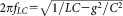 where L and C are the inductance and capacitance of the resonant circuit [Figure 4(b)]. The frequency of spontaneous oscillations was verified to decrease when the capacitance C is reduced [Figure 4(c,d)].

The spontaneous oscillations of composites are more complex than those generated by semiconductor multilayers. This can be seen in Figure 1(a), which shows multimode frequency generation. Spectral analysis of these oscillations36 reveals a natural mode of oscillations besides the driven oscillation mode set by the LC circuit. By varying L and C it is possible to make the composite oscillate over a 0–25 kHz bandwidth. The upper limit of this range corresponds to the intrinsic cut-off capacitance of the composite, which depends on the HOPG filling fraction. In contrast to the driven mode, the natural mode is self-oscillations of the composite, which occur in the NDR region without any external circuit. This mode is independent of L or C and is observed even after these components have been removed. The natural mode usually oscillates at a frequency higher than the cut-off frequency of the driven mode. The same bimodal frequency generation has been observed in several composites. The frequency of the natural mode increases with increasing pressure and graphite filling fraction. The natural mode is ascribed to drip-like percolation through the composite.36
Having demonstrated the active properties of the material, the next step is to investigate electrical behavior when the material is deformed. To this end, Littlejohn et al.36 have synthesized graphite-silicone thin Hall bars on stretchable and bendable substrates which are shown in Figure 5(a–c), respectively. The Hall bar in Figure 5(a) was prepared by imprint lithography and overlaid on pristine silicone substrate. Silicone substrates allow stretchable devices. The imprint mask consisted Hall bars molds prepared by optical lithography and plasma etched to a depth of 200 μm. The mask was coated with silicone oil to facilitate extrusion. The graphite silicone composite was then applied to fill the groovy pattern using a plastic blade. A uniform film of pristine silicone was then compression molded at the surface of the imprint mask to form a flexible substrate for the composite Hall bars. The pristine silicone/composite bilayer was allowed to set for 24 h to form rubber, after which the silicone bilayer was peeled giving the devices shown in Figure 5(a,b). Through this technique it is possible to fabricate silicone/silicone composite circuits of very small dimensions. The Hall bars prepared by Littlejohn et al.36 had channel widths down to 50 μm. The other types of composite devices are shown in Figure 5(c). These were molded on cellulose acetate sheets using similar methods. Cellulose acetate substrates bend but do not stretch given that their Young's modulus (E = 400 MPa) is much larger than that of silicone (E = 4 MPa). The composite/acetate bilayer was then bent to apply controlled interfacial strain ε [Figure 5(c)]. The bilayer strain was calculated from the relative change in the chord
 using Timoschenko's formula.136 The interfacial stress at 300 K was calculated form Stoney's formula.137

Increasing the strain has the effect of lowering the composite resistance and decreasing the negative differential conductance g, see Figure 5(c). The reduction of g is observed whether the composite film is put in tension or compression. This attribute of the electromechanical response has also been reported in silicon membranes.1, 138 The peak position moves to higher bias voltage with increasing strain. However, as long as the composite remains biased in the NDR region, the composite continues to oscillate. In fact, strain makes these oscillations easier to observed because the condition |g|r < 1 is relaxed. The low temperature experiments require the composite to be cooled down at 77 K and then warmed up to room temperature for the curvature of the film to be increased. The I–V curves were measured again after decreasing the curvature of the composite from bent to flat. The data in Ref. 36 show that the composite is remarkably resilient to temperature and mechanical cycling. Although the low temperature strain is very similar to the one applied at room temperature, low temperature stress is unknown in particular as silicone crosses its glass transition temperature at 230°C each time.
 , while the natural oscillation mode (labeled B) has no dependency dependence on
 . Strain affects the both oscillation modes via the reduction in negative differential conductance, g, as seen in Figure 5(d). First, strain increases the cut-off frequency of the cavity mode. The cut-off frequency is given by32:

 . Therefore, if
 , the cut-off frequency is
 and since g decreases with strain,
 will increase will increasing strain. Second, strain also increases the frequency of the natural mode, see line B in Figure 6(a–c). In this mode, the composite behaves as a strain sensor that encodes strain into frequency. The empirical frequency-strain relationship is plotted in Figure 6(d) and is approximately linear with a slope of
 Hz/% strain. It is interesting to compare the frequency response of the composite with the change in frequency of mechanoreceptor neurons in the skin (Merkel cells).40, 41 Figure 6(e) shows the voltage oscillations induced in one such receptor during the time interval in which pressure is applied to the skin.40 The frequency response to an increasing force [Figure 6(f)] is qualitatively the same as that of the composite in Figure 6(d). This effect opens up the possibility that flexible NDR might be used to make artificial skins.
APPLICATIONS OF FLEXIBLE NDR
The observation of NDR in flexible composites is paving the way toward other classes of active devices. Littlejohn et al.36 have demonstrated voltage amplification by using the composite as the active element (−g) of the tuned amplified circuit of Figure 7(a). The circuit is able to amplify a 1 kHz signal with a gain determined by
 . The amplitude of the amplified signal in Figure 7(b) fluctuates over time due to nonlinearities in the material. However, the voltage gain varies according to the theoretical curve of the tuned amplifier when the series resistance r is varied.

Multilevel logic memories are another type of application for flexible NDR. These devices require the NDR material to be biased in the bistable regime, |g|r > 1, so that the load line of the external circuit intersects the I–V curve at more than one point. To obtain multiple stable levels, Capasso et al.33 and other groups87-89 have vertically integrated several double barrier resonant tunneling structures, which give multiple peaks in the I–V curves. A single load line intercepting these peaks obtains multiple stable states over a range of bias voltage [Figure 7(c)]. Van der Wagt et al.,89 Wei and Lin88 and Capasso et al.33 have demonstrated multiple level memory devices based on this principle. I–V curves with multiple peaks may also be obtained with composite materials. By integrating sections of composite film with graded HOPG filling fraction in series, as pictured in the inset to Figure 7(c), the peak current will be obtained at different values of the total applied voltage. The section with the lowest HOPG filling fraction will initially support the largest electric field and give the first current peak. The next current peak will occur in the section with the next higher HOPG filling fraction and so on. This concept may be used to design flexible multilevel memories.
CONCLUSION AND FUTURE DIRECTIONS
Perpendicular transport through graphene and h-boron nitride multilayers offers a novel route toward NDR based active electronics. The materials are cheap, flexible, atomically thin, and give NDR with higher peak-to-valley current ratios than semiconductor multilayers. NDR based on graphitic materials has successfully underpinned active properties such as pressure sensing or amplification. The NDR mechanism differ significantly from NDR in semiconductor multilayers in that momentum conservation and electrostatic feedback give asymmetric I–V curves in graphene/h-boron nitride/graphene and wide NDR regions (extending to break-down voltage) in graphite silicone composites. Two modes of oscillation have been identified in the NDR region of graphite-silicone composites. One of these modes does not require the composite to be embedded in a LC resonator, unlike semiconductor multilayers, which removes the main obstacle to scaling circuits incorporating NDR devices.
Future challenges revolve around identifying materials optimizing the peak-to-valley current ratio at room temperature. This necessarily requires engineering tunneling barriers to quench the thermo-activated current. Promising results have been obtained by functionalizing the graphene surface with NDI and PDI molecules or by growing defect free h-boron nitride/graphene junctions. Future NDR devices will also limit nonlinearities associated with Joule heating and increase their bandwidth to enable faster response. Past experiments suggest that both objectives may be reached through better control of material chemistry at the graphene-silicone, graphene-boron nitride interface. Physicists will equally need to gain further insight into the metal-insulator transition at the scale of individual HOPG nanoparticles and in small area structures.
ACKNOWLEDGMENTS
The author wishes to thank DSTL(UK) who has partially supported this work under grants CDE28143 and CDE32154.
Biography

Dr Alain Nogaret is associate professor at the University of Bath. He was awarded a Ph.D. in Physics on the magneto-tunneling spectroscopy of III-V semiconductor multilayers from INSA Toulouse. He currently studies negative differential resistance in graphitic compounds and spin dynamics in magnetically modulated two-dimensional electron systems. He has demonstrated robust negative differential resistance in flexible composites which he uses to make flexible amplifiers and strain sensors. He has also demonstrated commensurability oscillations in lateral magnetic superlattices, channeling by magnetic edge states, and electrically induced spin resonance.