DC–DC Power Converters
Abstract
DC–DC power converters employ switched-mode circuitry to change dc voltages and currents with efficiencies approaching 100%. Basic converter circuits can reduce the voltage (buck converter), increase the voltage (boost converter) or both (buck-boost, Cuk, and SEPIC converters). Transformer-isolated circuits include the bridge, forward, and flyback converters.
Loss mechanisms include conduction loss arising from resistances or forward voltage drops of the power components, and switching loss generated during the transistor and diode switching transitions. Synchronous rectifiers can be employed to reduce the significant conduction loss caused by diode forward voltage drops in low-voltage applications.
The discontinuous conduction mode may arise when the inductor current is sufficiently small, which causes the output voltage to be strongly load-dependent.
Voltage-mode control employs pulse-width modulation to regulate the converter output voltage or other quantities through variation of the transistor duty cycle. Another popular technique is current-mode control, in which a circuit eauses the peak transistor current to follow a control reference signal.
Averaging methods are commonly employed to model the dynamics and efficiency of dc–dc power converters. The state-space averaging method leads to an equivalent circuit model that predicts the converter small-signal transfer functions. The circuit averaging technique is easily applied to simulate the converter transfer functions, in both continuous and discontinuous conduction modes, using computer programs such as SPICE.
- 1 Introduction
- 2 Converter Circuit Topologies
- 3 Analysis of Converter Waveforms
- 4 Transformer Isolation
- 5 Switch Implementation
- 6 Discontinuous Conduction Mode
- 7 Current-Mode Control
- 8 DC-DC Converter Modeling
1 Introduction
Direct current–direct current (dc–dc) power converters are employed in a variety of applications, including power supplies for personal computers, office equipment, spacecraft power systems, laptop computers, and telecommunications equipment, as well as dc motor drives. The input to a dc–dc converter is an unregulated dc voltage Vg. The converter produces a regulated output voltage V, having a magnitude (and possibly polarity) that differs from Vg. For example, in a computer off-line power supply, the 120 V or 240 V ac utility voltage is rectified, producing a dc voltage of approximately 170 V or 340 V, respectively. One or more dc-dc converters then reduce the voltage to the regulated several volts required by the processor integrated circuits (ICs).
High efficiency is invariably required because cooling of inefficient power converters is difficult and expensive. The ideal dc–dc converter exhibits 100% efficiency; in practice, efficiencies of 70% to 95% are typically obtained. This is achieved using switched-mode, or chopper, circuits whose elements dissipate negligible power. Pulse-width modulation (PWM) allows control and regulation of the total output voltage. This approach is also employed in applications involving alternating current, including high-efficiency dc–ac power converters (inverters and power amplifiers), ac–ac power converters, and some ac–dc power converters (low-harmonic rectifiers).
1.1 Power Stage Operation
A basic dc–dc converter circuit known as the buck converter is illustrated in Fig. 1 (1-5) A single-pole double-throw (SPDT) switch is connected to the dc input voltage Vg as shown. The switch output voltage vs(t) is equal to Vg when the switch is in position 1 and is equal to zero when the switch is in position 2. The switch position varies periodically, such that vs(t) is a rectangular waveform having period Ts and duty cycle D. The duty cycle is equal to the fraction of time that the switch is connected in position 1, and hence,  . The switching frequency fs is equal to
  . In practice, the SPDT switch is realized using semiconductor devices such as diodes, power metal-oxide-semiconductor field-effect transistors (MOSFETs), insulated-gate bipolar transistors (IGBTs), bipolar junction transistors (BJTs), or thyristors. Typical switching frequencies lie in the range 1 kHz to 1 MHz, depending on the speed of the semiconductor devices.

The buck converter consists of a switch network that reduces the dc component of voltage and a low-pass filter that remove the high-frequency switching harmonics: (a) schematic and (b) switch voltage waveform.
 (1)
(1) , the dc component of Vs is less than or equal to Vg.
The power dissipated by the switch network is ideally equal to zero. When the switch contacts are closed, then the voltage across the contacts is equal to zero and hence the power dissipation is zero. When the switch contacts are open, then there is zero current and the power dissipation is again equal to zero. Therefore, the ideal switch network can change the dc component of voltage without dissipation of power.
 . A low-pass filter is employed for this purpose. The converter of Fig. 1 contains a single-section L-C low-pass filter. The filter has corner frequency f0 given by
 (2)
(2) (3)
(3) (4)
(4)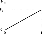
Buck converter dc output voltage V vs. duty cycle D.
Figure 3 illustrates one way to realize the switch network in the buck converter, using a power MOSFET and diode. A gate drive circuit switches the MOSFET between the conducting (on) and blocking (off) states, as commanded by a logic signal  . When
  is high (for
  ), then MOSFET
  conducts with negligible drain-to-source voltage. Hence,
  is approximately equal to Vg, and the diode is reverse-biased. The positive inductor current
  flows through the MOSFET. At time
  ,
,  becomes low, commanding MOSFET Q1 to turn off. The inductor current must continue to flow; hence,
  forward-biases diode
  and
and  is now approximately equal to zero. Provided that the inductor current iL(t) remains positive, then diode D1 conducts for the remainder of the switching period. Diodes that operate in the manner are called freewheeling diodes.
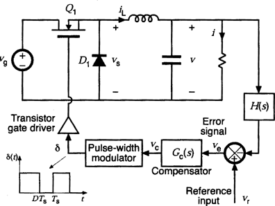
Realization of the ideal SPDT switch using a transistor and freewheeling diode. In addition, a feedback loop is added for regulation of the output voltage.
1.2 PWM Control System
As the converter output voltage v(t) is a function of the switch duty cycle D, a control system can be constructed that varies the duty cycle to cause the output voltage to follow a given reference vr. Figure 3 illustrates the block diagram of a simple converter feedback system. The output voltage is sensed using a voltage divider and is compared with an accurate dc reference voltage vr. The resulting error signal is passed through an op-amp compensation network. The analog voltage vc(t) is next fed into a PWM. The modulator produces a switched voltage waveform that controls the gate of the power MOSFET  . The duty cycle D of this waveform is proportional to the control voltage vc(t). This approach is sometimes called voltage-mode control.
If this control system is well designed, then the duty cycle is automatically adjusted such that the converter output voltage v follows the reference voltage vr and is essentially independent of variations in vg or the load current. Because the PWM samples vc(t) at a rate equal to the switching frequency  the feedback system generally is designed such that its bandwidth is substantially slower than the switching frequency.
2 Converter Circuit Topologies
A large number of dc–dc converter circuits is known that can increase or decrease the magnitude of the dc voltage and/or invert its polarity (1-5). Figure 4 illustrates several commonly used dc–dc converter circuits, along with their respective conversion ratios. In each example, the switch is realized using a power MOSFET and diode; however, other semiconductor switches such as IGBTs, BJTs, or thyristors can be substituted if desired.
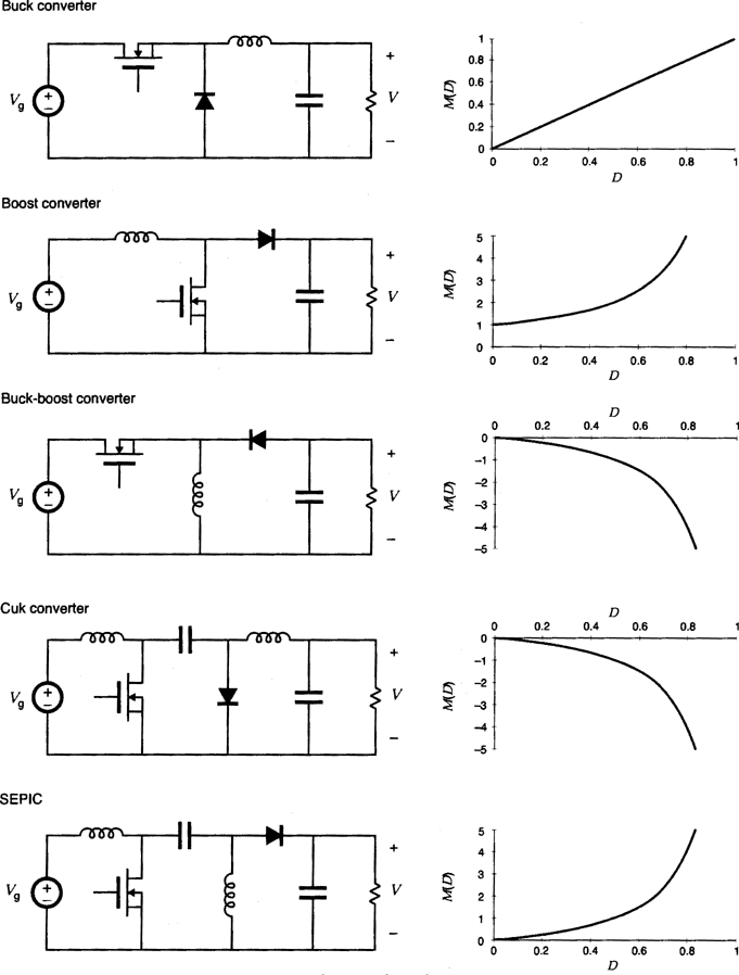
Several basic dc–dc converters and their dc conversion ratios  .
.
The first converter is the buck converter, which reduces the dc voltage and has conversion ratio  . In a similar topology known as the boost converter, the positions of the switch and inductor are interchanged. This converter produces an output voltage V that is greater in magnitude than the input voltage Vg. Its conversion ratio is
  .
.
In the buck-boost converter, the switch alternately connects the inductor across the power input and output voltages. This converter inverts the polarity of the voltage and can either increase or decrease the voltage magnitude. The conversion ratio is  .
.
The Cuk converter contains inductors in series with the converter input, and output ports. The switch network alternately connects a capacitor to the input and output inductors. The conversion ratio M(D) is identical to that of the buck-boost converter. Hence, this converter also inverts the voltage polarity, while either increasing or decreasing the voltage magnitude.
The single-ended primary inductance converter (SEPIC) can also either increase or decrease the voltage magnitude. However, it does not invert the polarity. The conversion ratio is  .
.
3 Analysis of Converter Waveforms
Under steady-state conditions, the voltage and current waveforms of a dc–dc converter can be found by use of two basic circuit analysis principles. The principle of inductor volt-second balance states that the average value, or dc component, of voltage applied across an ideal inductor winding must be zero. This principle also applies to each winding of a transformer or other multiple winding magnetic devices. Its dual, the principle of capacitor amp-second or charge balance, states that the average current that flows through an ideal capacitor must be zero. Hence, to determine the voltages and currents of dc–dc converters operating in periodic steady state, one averages the inductor current and capacitor voltage waveforms over one switching period and equates the results to zero.
The equations are greatly simplified by use of a third artifice, the small ripple approximation. The inductor currents and capacitor voltages contain dc components, plus switching ripple at the switching frequency and its harmonics. In most wel-designed converters, the switching ripple is small in magnitude compared with the dc components. For inductor currents, a typical value of switching ripple at maximum load is 10% to 20% of the dc component of current. For an output capacitor voltage, the switching ripple is typically required to be much less than 1% of the dc output voltage. In both cases, the ripple magnitude is small compared with the dc component and can be ignored.
As an example, consider the boost converter of Fig. 5(a). A resistor RL is included in series with the inductor, to model the resistance of the inductor winding. It is desired to determine simple expressions for the output voltage V, inductor current IL, and efficiency  . Typical inductor voltage and capacitor current waveforms are sketched in Fig. 5(b).

A nonideal boost converter: (a) schematic and (b) inductor voltage and capacitor current waveforms.
With the switch in position 1, the inductor voltage is equal to  . By use of the small ripple approximation, we can replace
  with its dc component
  and hence obtain
  . Likewise, the capacitor current is equal to
  , which can be approximated as
  .
.
When the switch is in position 2, the inductor is connected between the input and the output voltages. The inductor voltage can now be written  . The capacitor current can be expressed as
  .
.
 must be equal to zero. Upon equating the average value of the
  waveform of Fig. 5(b) to zero, we obtain
 (5)
(5) (6)
(6) (7)
(7) (8)
(8) . In the ideal case, when
  , the voltage conversion ratio M(D) is equal to one at
  and tends to infinity as D approaches one. In the practical case where some small inductor resistance RL is present, the output voltage tends to zero at
  . In addition, it can be observed that the inductor winding resistance RL (and other loss elements as well) limits the maximum output voltage that the converter can produce. Obtaining a given large value of
  requires that the winding resistance RL be sufficiently small.
Output voltage vs. duty cycle, for the nonideal boost converter of Fig. 5.
 (9)
(9) (10)
(10) . It can be observed that to obtain high efficiency, the inductor winding resistance RL should be much smaller than
  . This is much easier to accomplish at low duty cycles, where (
 ) is close to unity, that at high duty cycles where (
 ) approaches zero. Consequently, the efficiency is high at low duty cycles but decreases rapidly to zero near
  . This behavior is typical of converters having boost or buck-boost characteristics.
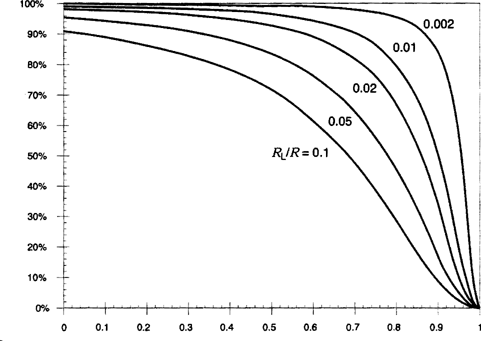
Efficiency vs. duty cycle, for the nonideal boost converter of Fig. 5.
Semiconductor conduction losses, caused by the on-resistances or forward voltage drops of the semiconductor switching elements, can be modeled in a similar manner. Semiconductor switching losses arise during the switching transitions when the SPDT switch changes from position 1 to position 2 or vice versa and are described in more detail below.
4 Transformer Isolation
In many applications, it is desired to incorporate a transformer into the switching converter, to obtain dc isolation between the converter input and output. For example, in off-line power supply applications, isolation is usually required by regulatory agencies. This isolation could be obtained by simply connecting a 50 Hz or 60 Hz transformer at the power supply ac input terminals. However, as transformer size and weight vary inversely with frequency, incorporation of the transformer into the converter can make significant improvements: the transformer then operates at the converter switching frequency of tens or hundreds of kilohertz. The size of modern ferrite power transformers is minimized at operating frequencies ranging from several hundred kilohertz to roughly one Megahertz. These high frequencies lead to dramatic reductions in transformer size.
When a large step-up or step-down conversion ratio is required, the use of a transformer can allow better converter optimization. By proper choice of the transformer turns ratio, the voltage or current stresses imposed on the transistors and diodes can be minimized, which leads to improved efficiency and lower cost.
Multiple dc outputs can also be obtained in an inexpensive manner, by adding multiple secondary windings and converter secondary-side circuits. The secondary turns ratios are chosen to obtain the desired output voltages. Usually, only one output voltage can be regulated, via control of the converter duty cycle, so wider tolerances must be allowed for the auxiliary output voltages. Cross regulation is a measure of the variation in an auxiliary output voltage, given that the main output voltage is regulated perfectly.
The basic operation of transformers in most power converters can be understood by replacing the transformer with the simplified model illustrated in Fig. 8(b). The model neglects losses and imperfect coupling between windings; such phenomena are usually considered to be converter nonidealities. The model consists of an ideal transformer plus a shunt inductor known as the magnetizing inductance LM. This inductor models the magnetization of the physical transformer core, and hence, it must obey all of the usual rules for inductors. In particular, volt-second balance must be maintained on the magnetizing inductance. Furthermore, as the voltages of all windings of the ideal transformer are proportional, volt-second balance must be maintained for each winding. Failure to achieve volt-second balance leads to transformer saturation and, usually, destruction of the converter. The means by which transformer volt-second balance is achieved is known as the transformer reset mechanism.

Modeling a physical transformer such that its basic operation within an isolated dc–dc converter can be understood: (a) transformer schematic symbol and (b) equivalent circuit model that includes magnetizing inductance LM and an ideal transformer.
There are several ways of incorporating transformer isolation into any dc–dc converter. The full-bridge, half-bridge, forward, and push-pull converters are commonly used isolated versions of the buck converter. Similar isolated variants of the boost converter are known. The flyback converter is an isolated version of the buck-boost converter. Isolated variants of the SEPIC and Cuk converter are also known. The full-bridge, forward, and flyback converters are briefly described in this section.
4.1 Full-Bridge Buck-Derived Converter
The full-bridge transformer-isolated buck converter is sketched in Fig. 9. Typical waveforms are illustrated in Fig. 10.

The full bridge transformer-isolated buck converter.

Waveforms of the full bridge circuit of Fig. 9.
The transformer primary winding is driven symmetrically, such that the net volt-seconds applied over two switching periods is equal to zero. During the first switching period, transistors Q1, and Q4 conduct for time DTs. The volt-seconds applied to the primary winding during this switching period are equal to  . During the following switching period, transistors Q2 and Q3 conduct for time DTs, thereby applying
  volt-seconds to the transformer primary winding. Over two switching periods, the net applied volt-seconds is equal to zero.
In practice, small imbalances exist such as the small differences in the transistor forward voltage drops or transistor switching times, so that the average primary winding voltage is small but nonzero. This nonzero dc voltage can lead to transformer saturation and destruction of the converter. Transformer saturation under steady state conditions can be avoided by placing a capacitor in series with the transformer primary. Imbalances then induce a dc voltage component across the capacitor, rather than across the transformer primary. Another solution is the use of current-mode control; the series capacitor is then omitted.
 (11)
(11)The full bridge configuration is typically used in switching power supplies at power levels of several hundred watts or greater. At lower power levels, approaches such as the forward converter are preferred because of their lower parts count. Four transistors and their associated drive circuits are required. The utilization of the transformer is good, which leads to small transformer size. The transformer operating frequency is one half of the transistor switching frequency.
4.2 Forward Converter
The forward converter is illustrated in Fig. 11. This transformer-isolated converter is also based on the buck converter. It requires a single transistor and therefore finds application at power levels lower than those encountered in the full bridge circuit. The maximum transistor duty cycle is limited in value; for the common choice  , the duty cycle is limited to the range
  .
.
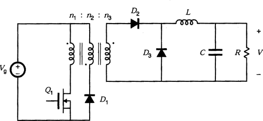
The forward converter, a single-transistor isolated buck converter.
 is applied to the second winding. This negative voltage causes the magnetizing current to decrease. When the magnetizing current reaches zero, diode D1x turns off. Volt-second balance is maintained on the transformer windings provided that the magnetizing current reaches zero before the end of the switching period. It can be shown that this occurs when
 (12)
(12) this expression reduces to
 (13)
(13) (14)
(14)A two-transistor version of the forward converter is illustrated in Fig. 12. Transistors Q1 and Q2 are controlled by the same gate drive signal, such that they conduct simultaneously. After the transistors turn off, the transformer magnetizing current forward-biases diodes D1 and D2. This applies voltage  across the primary winding, thereby resetting the transformer. The duty cycle is again limited to
  This converter has the advantage that the transistor peak blocking voltage is limited to Vg and is clamped by diodes D1 and D2. This circuit is quite popular in power supplies having 240 Vac inputs.

A two-transistor version of the forward converter.
4.3 Flyback Converter
The flyback converter of Fig. 13 is based on the buck-boost converter. Although the two-winding magnetic device is represented using the same symbol as the transformer, a more descriptive name is “two-winding inductor.” This device is sometimes also called a “flyback transformer.” Unlike the ideal transformer, current does not flow simultaneously in both windings of the flyback transformer. Rather, the flyback transformer magnetizing inductance assumes the role of the inductor of the buck-boost converter. The magnetizing current is switched between the primary and the secondary windings.

The flyback converter, a single-transistor isolated buck-boost converter.
When transistor Q1 conducts, diode D1 is reverse-biased. The primary winding then functions as an inductor, connected to the input source Vg. Energy is stored in the magnetic field of the flyback transformer. When transistor Q1 turns off, the current ceases to flow in the primary winding. The magnetizing current, referred to the secondary winding, now forward-biases diode D1. Energy stored in the magnetic field of the flyback transformer is then transferred to the dc load.
 (15)
(15)The flyback converter has traditionally been used in the high-voltage power supplies of televisions and computer monitors. It also finds widespread application in switching power supplies with power levels of tens of watts. This converter has the advantage of a very low parts count. Multiple outputs can be obtained using a minimum number of added elements: Each auxiliary output requires only an additional winding, diode, and capacitor. However, in comparison with buck-derived transformer-isolated converters such as the full bridge and forward circuits, the flyback converter has the disadvantage of poor cross regulation.
5 Switch Implementation
The switch network realization of Fig. 3 employs single-quadrant switches. Each semiconductor element can conduct current of only one polarity in the on state and block voltage of one polarity in the off state, which implies that, for proper functioning of the switch network, the source voltage, load voltage, and inductor current must all be positive. Consequently, the switch network allows the instantaneous power to flow in one direction only: from the source Vg toward the load.
Bidirectional (regenerative) power flow can be obtained with a current-bidirectional two-quadrant realization of the switch network. An example is illustrated in Fig. 14, in which a dc–dc converter interfaces batteries to the main dc power bus of a spacecraft. The anti-parallel-connected transistors and diodes form current-bidirectional switches. Transistor Q2 is driven with the complement of the Q1 drive signal, such that Q2 is off when Q1 is on, and vice versa. To charge the battery, the inductor current  is positive and flows through transistor Q1 and diode D2. To discharge the battery, the current
  reverses polarity and flows through transistor Q2 and diode
  . In both cases, the battery voltage is less than the main dc bus voltage. The magnitude and polarity of the battery current can be controlled via adjustment of the duty cycle D.
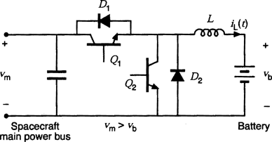
A buck converter with two-quadrant switches and bidirectional power flow. Spacecraft battery charger/discharger example.
Synchronous rectifiers are commonly employed in dc–dc converters that supply a low voltage such as the one or two volts required by computer processors. In such applications, the approximately fixed diode forward voltage drop leads to considerable loss. The efficiency can be improved by replacing the diode with a MOSFET Q2 having low on-resistance, as illustrated in Fig. 15. The forward voltage drop can then be made as small as desired if a large MOSFET having sufficiently small on resistance is employed. The synchronous rectifier exploits the ability of the power MOSFET to conduct reverse current; the gate of transistor Q2 should be driven so that Q2 turns on when the diode would have turned on.

Buck converter employing synchronous rectifier Q2.
Switching loss imposes an upper limit on the switching frequencies of practical converters. During the switching transitions, the transistor voltage and current are simultaneously large. In consequence, the transistor experiences high instantaneous power loss, which can lead to significant average power loss, even though the switching transitions are short in duration. Switching loss causes the converter efficiency to decrease as the switching frequency is increased.
Several mechanisms lead to switching loss. Significant energy can be lost during the slow switching times of minority-carrier semiconductor devices such as BJTs, IGBTs, and thyristors. The p-n diode reverse recovery process induces substantial additional energy loss in the transistor during the transistor turn-on transition. The energy stored in the semiconductor output capacitances is dissipated during the transistor turn-on transition. Energy stored in transformer leakage inductances and other stray inductances is usually dissipated by the transistor during the turn-off transition. The total switching loss is equal to the sum of the energy losses that arise via these mechanisms, multiplied by the switching frequency. Switching loss can be partially mitigated through the use of a resonant or soft-switching converter.
6 Discontinuous Conduction Mode
When the switching ripple in an inductor current or capacitor voltage is large enough to cause the polarity of the applied switch voltage or current to reverse, then converters that employ single-quadrant switches enter the discontinuous conduction mode (DCM), which typically occurs at light load (small load current) in dc–dc converters that employ diodes rather than synchronous rectifiers. In some cases, dc–dc converters are purposely designed to operate in DCM at all load currents.
The properties of dc–dc converters change radically when DCM is entered. The conversion ratio M(D) becomes load-dependent. The output voltage is increased, and the small-signal converter dynamics are altered substantially. Control of the output voltage may be lost when the load is removed; indeed, the output voltages of boost and buck-boost converters tend to very large values when the load is disconnected.
 is greater than the dc component I, and hence, the diode becomes reverse-biased at time
  . The remainder of the switching period constitutes a third subinterval in which both the transistor and the diode are off. It can be shown that the condition for operation in DCM can be expressed as
 (16)
(16) and
and  for the buck converter. In general, the DCM boundary can be expressed with an equation in this form; the expressions for
  for basic converters are listed in Table 1. When equation 16 is not satisfied, then the converter operates in the continuous conduction mode (CCM) as described by Fig. 1 and equation 4.
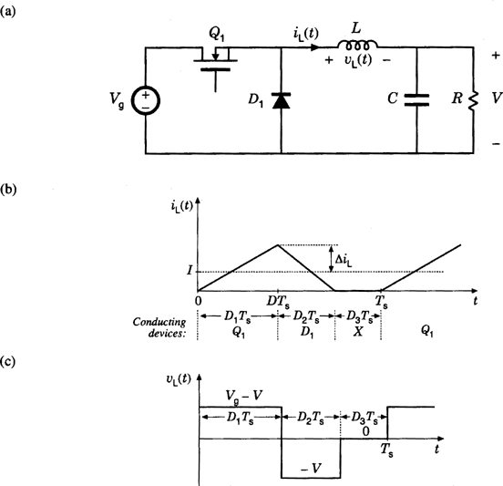
Operation of the buck converter in the discontinuous conduction mode: (a) schematic, (b) inductor current waveform, and (c) inductor voltage waveform.
Converter |
|
|
CCM M(D) |
|
|
DCM M(D) |
|
|
K |
|
|
|
|---|---|---|---|---|---|---|---|---|---|---|---|---|
Buck |
|
|
D |
|
|
|
|
|
|
|
|
|
|
||||||||||||
Boost |
|
|
|
|
|
|
|
|
|
|
|
|
|
||||||||||||
Buck-boost |
|
|
|
|
|
|
|
|
|
|
|
|
|
||||||||||||
Cuk |
|
|
|
|
|
|
|
|
|
|
|
|
|
||||||||||||
SEPIC |
|
|
|
|
|
|
|
|
|
|
|
|
 of Fig. 16(c), this leads to
 (17)
(17) (18)
(18) (19)
(19) . Table 1 summarizes the steady-state characteristics for the converters of Fig. 4. Note that, for the Cuk and SEPIC topologies, the parameter K depends on the parallel combination of the two inductor values
  .
.7 Current-Mode Control
In the voltage-mode control approach of Fig. 3, the pulse-width modulator drives the transistor at a duty cycle that is a direct function of the control signal. A popular alternative approach is current-mode control, in which a mixed-signal control circuit that causes the switch current to follow a control signal replaces the pulse-width modulator (6-9). Both peak-current and average-current controllers are available commercially.
The principal advantage of current-mode control is its simpler dynamics. Effectively, the controller employs current feedback information; this significantly reduces the influence of inductor dynamics on the converter small-signal transfer functions and transient response. Although current-mode control requires sensing of the switch or inductor current, such current sensing is normally present anyway, in conjunction with overcurrent protection circuitry. Current-mode control can also reduce or eliminate transformer saturation problems in isolated dc–dc converters such as the full bridge or push–pull topologies.
Figure 17 illustrates elements of a current-mode controlled buck converter. A latch is set by a clock signal at the beginning of each switching period, turning on transistor Q1. This applies positive voltage across the inductor, which causes the inductor current and the transistor current to increase. A sensor circuit produces a signal  that is proportional to the switch current
  . When this signal is equal to a control signal
  , the latch is reset and the current-mode controller turns off the transistor switch. In consequence, the peak transistor current, and the peak inductor current, follow the control signal
  . The control signal
  is typically generated by an output voltage controller as illustrated in Fig. 17. Additionally, an “artificial ramp” may be required for stabilization of the current-mode controller, particularly at operating points that require a duty cycle greater than 0.5.
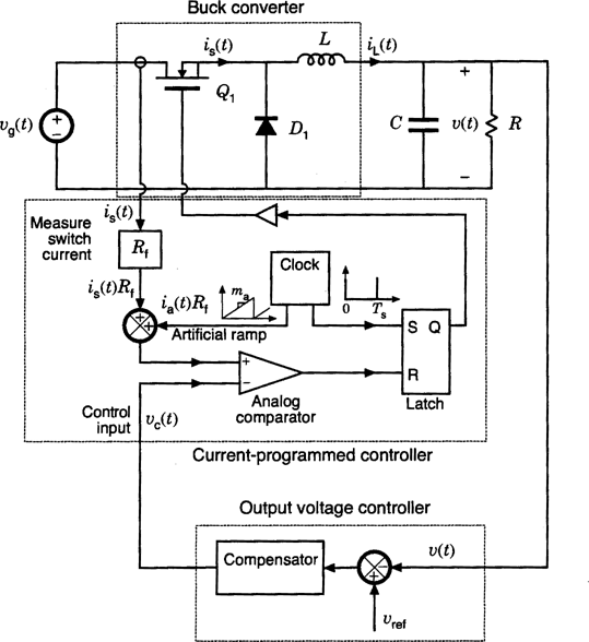
Elements of a current-mode controlled buck converter.
8 DC-DC Converter Modeling
To design the control system of a converter, it is necessary to model the converter dynamic behavior. In particular, it is of interest to determine how variations in the power input voltage  , the load current, and the duty cycle d(t) affect the output voltage. Unfortunately, understanding of converter dynamic behavior is hampered by the nonlinear time-varying nature of the switching and pulse-width modulation process. These difficulties can be overcome through the use of waveform averaging and small-signal modeling techniques (10-15). A well-known converter modeling technique known as state-space averaging is briefly described here. An equivalent approach known as averaged switch modeling is also described; this approach is well suited to computer simulation. Results for several basic converters are listed in tabular form.
8.1 State-Space-Averaging
The state-space averaging technique generates the low-frequency small-signal ac equations of PWM dc–dc converters. Converter transfer functions and equivalent circuit models can be obtained.
 , the converter reduces to a linear circuit whose equations can be written in the following state-space form:
 (20)
(20) (21)
(21) .
. (22)
(22) (23)
(23) represents the norm of vector x.
 (24)
(24) (25)
(25) (26)
(26) (27)
(27)8.2 Simulation via Averaged Switch Modeling
In the averaged switch modeling approach, a switch network is defined that contains all switching elements of the converter. The low-frequency components of the terminal waveforms of the switch network are found, with the high-frequency switching harmonics discarded via a process known as averaging. The result is a time-invariant network that models the dc and low-frequency ac components of the converter waveforms. The converter small-signal transfer functions can be found using this model. In addition, the model allows efficient simulation of the converter dynamics using a conventional program such as SPICE (3, 16-18).
Consider the buck-boost converter of Fig. 18. The transistor and diode switching elements are grouped into a two-port switch network, and the remainder of the converter circuit is linear and time-invariant. For this example, the terminal waveforms of the switch network are taken to be the MOSFET drain-to-source voltage  , the MOSFET drain current
  , the diode anode-to-cathode voltage
  , and the diode cathode current
  . These terminal waveforms are sketched in Fig. 19, for operation in the continuous conduction mode.
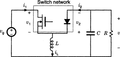
Averaged switch modeling of a buck-boost converter

Waveforms of the switch network of Fig. 18.
Next, we assume that the natural time constants of the converter circuit are much longer than the switching period Ts, so that the converter effectively low-pass filters the switching harmonics. When this assumption is satisfied, then one may average the waveforms over a period that is short compared with the system natural time constants without significantly altering the system response (12). In particular, averaging over the switching period Ts removes the switching harmonics while preserving the underlying low-frequency components of the converter waveforms. This step removes the small but mathematically complex switching harmonics, which leads to a relatively simple and tractable dc and ac converter model. In practice, we need only average the waveforms of the switch network, because switching harmonics are not generated in the remainder of the converter.
 of a waveform
  is
is
 (28)
(28) (29)
(29) (30)
(30)Equation 30 suggests that the switch network could be modeled by one of the equivalent circuits of Fig. 20. Figure 20(b) illustrates replacement of the transistor and diode with dependent voltage and current sources according to equation 30; this model is useful for SPICE simulation. Equivalently, an ideal dc transformer, denoted by a transformer symbol having a solid horizontal line, can replace the dependent sources as illustrated in Fig. 20(c). The dc transformer model has an effective turns ratio equal to  . It obeys all of the usual properties of transformers, except that it can pass dc voltages and currents. Although conventional magnetic-core transformers cannot pass dc voltages, we are nonetheless free to define an ideal dc transformer symbol; use of this symbol in modeling dc–dc converter properties is justified because it correctly predicts how the switch network converts dc and low-frequency ac voltages and currents, ideally with 100% efficiency.
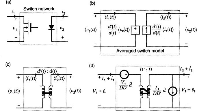
Evolution of the averaged switch model in CCM: (a) original switch network, (b) averaging the waveforms, (c) large-signal transformer model, and (d) small-signal ac model.
The transformer model of Fig. 20(c) is a time-varying element because its effective turns ratio depends on the control input d(t). For analysis of converter transfer functions, it is necessary to linearize this element in a manner similar to that employed in equations 22 and 23. The result is the small-signal switch model of Fig. 20(d). In any of the basic converters, such as those of Fig. 4, the transistor and diode can be replaced by the model of Fig. 20(d), which results in a small-signal equivalent circuit that predicts the small-signal transfer functions of the converter.
 (31)
(31) (32)
(32)An averaged switch model that implements the above equations in PSPICE is illustrated in Fig. 21. The model terminals 1-2 and 3-4 replace the transistor and diode, respectively. Terminal 5 is the duty cycle input; the duty cycle d is represented by a voltage in the range [0,1]. The model automatically switches between CCM and DCM, and can be applied to dc, ac, or transient simulation of single-transistor PWM converters.

Averaged switch model for converter simulation: (a) schematic entry symbol, (b) electrical circuit, and (c) PSPICE code.
8.3 Canonical Model
Equivalent circuit models of dc–dc converters can be constructed using the state-space averaged equations 24 and 27 or by manipulation or the averaged switch models above, As all PWM dc–dc converters perform similar basic functions, one finds that the equivalent circuit models have the same form. Consequently, the canonical circuit model of Fig. 22 can represent the physical properties of PWM dc–dc converters (10).

The canonical model: a small-signal equivalent circuit that models dc–dc converter dynamics and transfer functions.
The primary function of a dc–dc converter is the transformation of dc voltage and current levels, ideally with 100% efficiency. As in the averaged switch model described above, this function is represented in the model by an ideal dc transformer, denoted by a transformer symbol having a solid horizontal line. The dc transformer model has an effective turns ratio equal to the converter quiescent conversion ratio M(D).
Small ac variations in the source voltage  are also transformed by the conversion ratio M(D). Hence, a sinusoidal line is added to the dc transformer symbol, to denote that it also correctly represents how small-signal ac variations pass through the converter.
Small ac variations in the duty cycle d(t) excite ac variations in the converter voltages and currents. This is modeled by the  and
and  generators of Fig. 22. In general, both a current source and a voltage source are required.
The converter inductors and capacitors, necessary to low-pass filter the switching harmonics, also low-pass filter ac variations. The canonical model therefore contains an effective low-pass filter. Figure 22 illustrates the two-pole low-pass filter of the buck, boost, and buck-boost converters; complex converters having additional inductors and capacitors, such as the Cuk and SEPIC, contain correspondingly complex effective low-pass filters. The element values in the effective low-pass filter do not necessarily coincide with the physical element values in the converter. In general, the element values, transfer function, and terminal impedances of the effective low-pass filter can vary with quiescent operating point.
Canonical model parameters for the ideal buck, boost, and buck-boost converters are listed in Table 2. Transformer-isolated versions of the buck, boost, and buck-boost converters, such as the full bridge, forward, and flyback converters, can also be modeled using the equivalent circuit of Fig. 22 and the parameters of Table 2; one must then correctly account for the transformer turns ratio by referring all quantities to the transformer secondary.
Converter |
|
|
M(D) |
|
|
Le |
|
|
e(s) |
|
|
j(s) |
|---|---|---|---|---|---|---|---|---|---|---|---|---|
Buck |
|
|
D |
|
|
L |
|
|
|
|
|
|
|
||||||||||||
Boost |
|
|
|
|
|
|
|
|
|
|
|
|
|
||||||||||||
Buck-Boost |
|
|
|
|
|
|
|
|
|
|
|
|
8.4 Small-Signal Transfer Functions of the Buck, Boost, and Buck-boost Converters
 is the transfer function from d(s) to v(s), with
  set to zero. The line-to-output transfer function
  is the transfer function from
  to
to  , with d(s) set to zero. For the buck, boost, and buck-boost converters, these transfer functions can be written in the following forms:
 (33)
(33) (34)
(34) exhibits two poles but no zero. The line-to-output transfer functions of all three converters contain two poles and no zeroes.
Converter |
|
|
|
|
|
|
|
|
|
|
|
Q |
|
|
|
|---|---|---|---|---|---|---|---|---|---|---|---|---|---|---|---|
Buck |
|
|
D |
|
|
|
|
|
|
|
|
|
|
|
∞ |
|
|||||||||||||||
Boost |
|
|
|
|
|
|
|
|
|
|
|
|
|
|
|
|
|||||||||||||||
Buck-Boost |
|
|
|
|
|
|
|
|
|
|
|
|
|
|
|
The results of Table 3 can be applied to transformer-isolated versions of the buck, boost, and buck-boost converters, by referring all element values to the transformer secondary side. Equation 34 must also be multiplied by the transformer turns ratio.
The control systems of boost and buck-boost converters tend to be destabilized by the presence of the right-half plane (RHP) zero in the control-to-output transfer function. This occurs because, during a transient, the phase lag of the RHP zero causes the output to initially change in the wrong direction. When a RHP zero is present, it is difficult to obtain an adequate phase margin in conventional single-loop feedback systems having wide bandwidth. Prediction of the RHP zero, and the consequent explanation of why the feedback loops controlling continuous conduction mode boost and buck-boost converters tend to oscillate, was one of the early successes of averaged converter modeling and state-space averaging.


