Overview on Comparison of Four Preparation Methods and Physical Properties of Graphene
Abstract
Graphene is a single layer of carbon atoms arranged in a hexagonal lattice structure, forming a two-dimensional (2D) material with exceptional mechanical, electrical, and thermal properties. Graphene has emerged as one of the most promising nanomaterials because of its unique combination of exceptional properties: the thinnest and the strongest materials, an excellent conductor of electricity, and optically transparent as well. This article provides an overview of graphene materials regarding its basic structure, preparation methods, and unique properties. The four commonly used methods for preparing graphene are compared, and the advantages and disadvantages of each are expounded and briefly summarized. And the basic physical properties of graphene materials obtained by each method, namely, in mechanics, electricity, thermal, and optics, were elaborated in detail, and the related applications of graphene prospects are further discussed.
1. Introduction
Graphene is a novel two-dimensional (2D) honeycomb-structured carbon nanomaterial, which serves as an allotrope of carbon elements [1]. Graphene is composed of carbon atoms arranged in a hexagonal pattern, which are hybridized by sp2 to form a very stable structure. It is one of the thinnest and strongest nanomaterials with a sheet thickness of 0.34 nm, and the tensile strength and elastic modulus reached 130.5 GPa and 1.1 TPa, respectively, plus a hardness about 100 times higher than steel withstanding a maximum fracture pressure up to 29 N/m [2, 3].
Due to its unique structure, the maximum electron mobility of graphene at room temperature is 100 times as that of traditional silicon materials in the field of electronics, that is, electrical conductivity is over 1 × 10⁶ S/cm [4, 5]. Besides, graphene possesses excellent in-plane conductivity and thermal conductivity (up to 5300 W/m·K) and the electron mobility capped at 2 × 105 cm2/V·s at room temperature and exhibits a high gauge factor [6, 7] as well as unique advantages, for example, high carrier mobility, large specific area around 2630 m2/g, good flexibility, mechanical strength with Young’s modulus of ∼1 TPa, and biocompatibility [8–13]. The excellent properties of graphene in various aspects have attracted extensive attention from researchers and industrials; especially, the high-quality experimental development and adequate theoretical research on graphene have been carried out in various fields. The preparation of high-quality graphene is also inseparable from these theoretical studies and simulation development [14, 15]. All those excellent properties in varied aspects mentioned above have made graphene one of the most popular choices for developing top-notch sensors [16].
Graphene and its derivatives are shown in Figure 1 and mainly include single-layer graphene (SLG), few-layer graphene (FLG), graphene oxide (GO), reduced graphene oxide (rGO or RGO), and graphene nanosheets (GNS). Graphene is the name for a single-layer (monolayer) sheet of carbon atoms that are bonded together in a repeating pattern of hexagons. This sheet is only one atomic thick, and graphene sheets are building blocks for other graphitic materials, which could be cut and folded into a spherical shape to make a C60 fullerene molecule, even rolled up to make a carbon nanotube (CNT), and further bonded on top of each other to make the bulk material graphite.
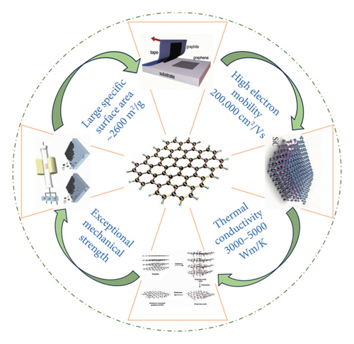
The structure and properties of a few layers of graphene (usually 2–10 layers) are not the same as those of bulk graphite and are closer to those of SLG; hence, they are collectively referred to as graphene [17]. GO and RGO or rGO are the most commonly used graphene derivatives [18, 19] for carbon material applications, such as sensors [20–22], supercapacitors [23, 24], anticorrosion coatings [25, 26], drug delivery [27, 28], DNA detection [29, 30], and solar cells [31, 32].
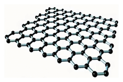
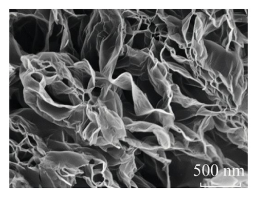
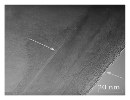
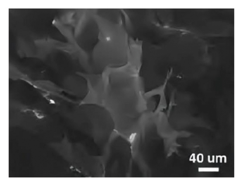
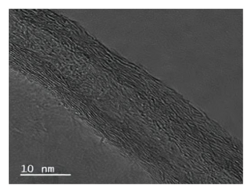
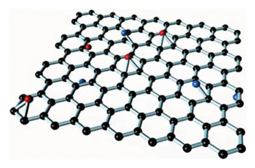
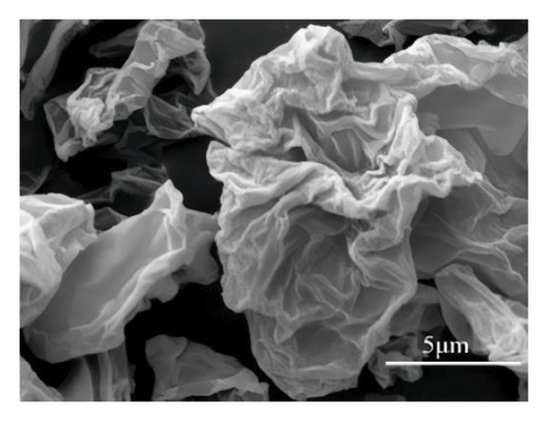
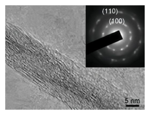
Looking closer at the chemical structure of graphene and its derivatives as detailed in Figures 2(a) and 2(b) [19, 33], that the surface of graphene has a thin gauze-like structure with a transparent and wrinkled surface, while the TEM images [19] in Figure 2(c) show that the graphene layers are light and thin with good transparency, accompanied with certain degree of wrinkles, which reduce the surface energy of graphene and increase its structural stability. GO as stated in Figures 2(d), 2(e), and 2(f) [34] illustrate a clear layered structure with thin and larger sizes, while the RGO or rGO exhibits a curled sheet-like structure with obvious wrinkles on the surface (Figures 2(g) and 2(h)) [33, 35]. In addition, the TEM image of RGO or rGO as illustrated in Figure 2(i) demonstrates a thin layer structure along with an orderly and neatly arranged graphite lattice [35].
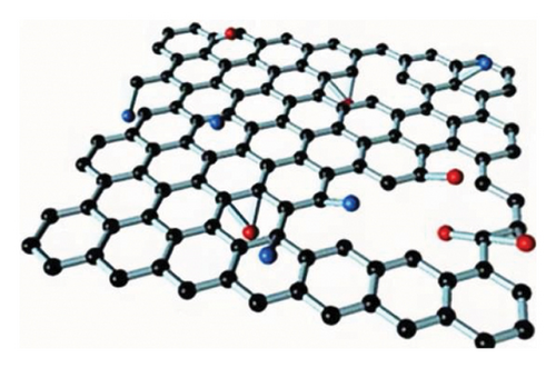
GO materials have abundant electronegative functional groups on their surfaces, such as hydroxyl and epoxy groups on both sides, while the carboxyl groups are attached to the edge. Although GO is a 2D material like graphene, its properties are very different from those of graphene, for instance, not absorbing visible light and very low electric conductance and significantly higher chemical activity as compared to that of graphene. Those oxygen-containing groups of GO are easy to form modified graphene oxide (MGO) through chemical coupling with active components for better loading and dispersion, which effectively improves the performance of composite materials as being considered as ideal carrier materials.
Reduced graphene is a type of carbon material produced by reducing oxidized graphene and has been widely studied and applied in various fields, for instance, biosensing, energy storage, solid-state capacitors, and semiconductors [36–40], agriculture, biomedicine, and sensors [41, 42], due to its unique characteristics such as bipolar charge and electron-rich properties, as compared to both graphene and oxidized graphene.
2. Methods for Graphene Fabrication
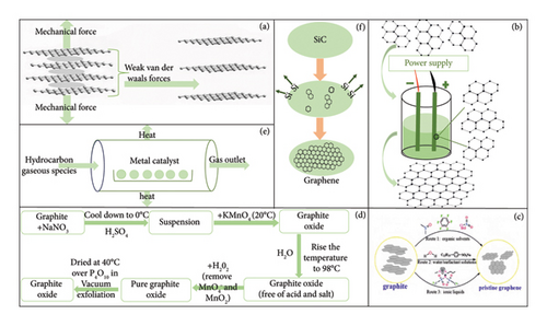
The methods of graphene preparation are receiving increasing attention from researchers and industrials in various fields, which in principle comes along with top-down and bottom-up approaches. The top-down method for preparing graphene typically requires exfoliation and reduction of the original graphite, which involve cutting the size from bulk to micro- or even nanoscale graphene derivatives. Among those methods for preparing graphene, exfoliation techniques and graphite oxide reduction methods are considered the most effective and widely used top-down methods. On the other hand, the bottom-up method typically relies on the use of hydrocarbons as precursors, such as chemical vapor deposition (CVD), epitaxial growth. The principles of several typical and commonly used methods for preparing graphene are portrayed in Figure 3 along with the advantages and disadvantages as summarized in Table 1, which is about to be elaborated in detail in the following sessions.
| Method | Technical principles | Advantages | Disadvantages | Ref. |
|---|---|---|---|---|
| Exfoliation techniques | Peeling the layer by overcoming the attraction forces to obtain the graphene | Simplest process | Size and defects uncontrollable, pollution | [44–49] |
| Redox | Strong oxidation treatment and separation by external stimulation, i.e., ultrasonication | Simple, low cost, low equipment requirements, and large-scale manufacturing | Unthoroughly graphite reduction and introduce ion impurities | [50–55] |
| CVD | Vaporized chemical reaction of a determined precursor and deposited on a substrate | Large scale, high quality, large area | High cost and difficulty in large-scale production | [56–58] |
| Epitaxial growth | A monocrystalline film deposited on a monocrystalline substrate | High quality and controllable size and thickness | Harsh conditions, high vacuum, high cost, and low efficiency | [17, 59–62] |
2.1. Top-Down Methods
2.1.1. Exfoliation Techniques
Graphene obtained via exfoliation methods could be achieved through mechanical exfoliation (Figure 3(a)), electrochemical exfoliation (Figure 3(b)), and liquid-phase exfoliation (Figure 3(c)). Among them, the mechanical peeling method mainly uses mechanical force to peel off the surface of fresh graphite crystals to obtain graphene layers followed by being transferred to the surface of the carrier [63]. For example, Novoselov [63] is the first introduced method by simply pressing the highly oriented pyrolytic graphite onto the photoresist layer of the glass substrate and forming thermal expansion between graphene layers via baking, and then the countertop was attached to the photoresist layer while the excess graphite sheets were removed by repeatedly being physically peeled off. Then, the glass substrate with attached microsheets was subjected to ultrasonication in acetone to further peel off thin-sheet graphene into the solution. When washed with excessive water and propanol, some thin sheets were captured on the surface of the wafer, which was later ascribed as SLG by using atomic force microscopy (AFM) technique. Afterward, several modified and simple exfoliation methods were developed for graphene layer preparation. For instance, a simple, scalable, and cost-effective method based on microfluidic technology using sodium salt of styrene maleic anhydride (SMA) copolymer as a stabilizer was developed to strip graphite into several layers of graphene in water [64]. An in situ shear exfoliation of graphite in PVA aqueous [65] was also explored for preparing high-quality, unoxidized thin-layer exfoliated graphene. And a simple wet ball milling strategy for achieving graphene exfoliation and functionalization simultaneously was applied for functionalized graphene preparation [66].
On top of that, electrochemical exfoliation is a promising method for producing graphene from bulk graphite, since an applied voltage drives ionic species to intercalate into graphite where they form gaseous species that expand and exfoliate individual graphene sheets [67]. Several factors might affect the effectiveness and efficiency of graphene production. In particular, an organic liquid-assisted electrochemical exfoliation using tetramethylammonium hydroxide (TMAH) as organic electrolyte [68] was developed for obtaining GNS, and the organic electrolyte eliminates the presence of unwanted metal ions on the GNS. It was also reported that the salt used influences the quality of the graphene, the surface functionality, thermal stability, and the degree of oxidation [69]. As of such, graphene with a particle size of 1 to 10 μm can be produced with a yield of about 65%, a high proportion of SLG, and a good electrical conductivity without further chemical reduction.
An ideal graphene sample generation in large quantities could be accomplished by the direct liquid-phase exfoliation of graphite to produce graphene, which is convenient but involves the use of colloidal suspensions, which is based on the one-step physical transformation of graphite into graphene exhibiting many unique advantages. Various liquids have been employed as exfoliation media and demonstrated a range of exfoliation efficiencies [43].
2.1.2. Oxidation–Reduction Method
The oxidation–reduction method mainly uses bulk graphite as starting material and strong acids for intercalating the graphite, then adds strong oxidants for oxidation that introduces oxygen-containing functional groups on the surface of graphene, so that the obtained GO could be dispersed in solution, and finally the graphene was achieved through further reduction methods (Figure 3(d)) [70]. Under the continuous research developments, several other methods for preparing oxidized graphite have been developed, including the classical Hummers method [71], Brodie method [72], and Staudenmaier method [71], the Hummers method of which is the currently most widely used. For example, Madhuri et al. [73] synthesized GO using the Hummers method by taking advantage of the vitamin C-rich nature of Phyllostachys officinalis, the pulp of which was ground, extracted, and dried into powder, followed by being heated in a suspension of GO for 30 min to obtain RGO or rGO. Zhao [74] prepared GO using an improved Hummers method in the mixture of distilled water and 10 mL of 30% H2O2, followed by 4 h of reaction under high temperature and high pressure, then the mixture was centrifuged, washed, and freeze-dried, and a porous RGO or rGO was obtained by thermal reduction at 300°C for 1 h. A novel and environment-friendly alternative system to produce graphene under minimum logistic and economic requirements was accomplished by using chemical oxidation with different types of bacteria [75], involving the bacterial strains or microbial consortia as biological reducing agents, which contributes significantly to the studies of obtaining graphene based on biological processes.
2.2. Bottom-Up Methods
2.2.1. CVD
The CVD (Figure 3(e)) method mainly uses carbon-containing compounds such as methane as a carbon source to grow graphene through high-temperature decomposition on the substrate surface [76]. The CVD method was initially mainly used to prepare semiconductor thin films and later was introduced for preparing graphene by Deokar et al. [77]. A SLG via CVD can be grown on the surface of platinum using ethylene as the raw material and thermal annealing method. Traditionally, using CH4 as carbon source, a precleaned copper foil was loaded into a CVD growth chamber and heated up under Ar/H2 mixture atmosphere. Subsequently, the CH4 gas was immediately charged for graphene growth. Afterward, the sample chamber was rapidly cooled to 700°C and further cooled to room temperature under the mixture of H2 and Ar environments. Later, high-crystalline quality SLG was obtained on the Cu foil substrate with significantly reduced processing time as compared to the traditional processes. By way of illustration, the quality and growth rate of graphene produced by using C2H6 as carbon source to grow graphene on copper foil at lower temperatures of 750°C [78] process are superior to those by the traditional processes using methane.
2.2.2. Epitaxial Growth
The possible earliest starting phase of epitaxial growth of graphene was found out by Badami [79] in 1962 by an intense heating of SiC in near-vacuum conditions, exhibiting a trace existence of graphene. Generally, this method uses SiC as the source and the Si atoms are sublimated much faster than the C atoms under a condition of high temperature and lower pressure, which leaves C only on its surface frame and further underwent a rearrangement and grow up to form graphene (Figure 3(f)). Later, ultrathin epitaxial graphite films typically composed of three graphene sheets were successfully grown by thermal decomposition on the (0001) surface of 6H-SiC [80]. Through this method, a high-quality epitaxial graphene (EG) on SiC was first demonstrated by the group of De Heer [81] in 2011 that encapsulated the silicon carbide crystal in a graphite shell to maintain a high Si vapor pressure, allowing for a growth close to thermodynamic equilibrium, resulting in high-quality EG.
Although the technology of graphene preparation by epitaxial method has made great progress and breakthroughs, researchers continue to explore and innovate it further. To give you an idea, Zhao et al. [82] proposed a method to overcome the low quality and high cost of graphene prepared by traditional epitaxial growth methods, which not only reduces preparation costs but also improves the quality of graphene epitaxial films. And through a well control over EG through face-to-face annealing of silicon carbide in ultra-high vacuum [83], the silicon atoms trapped in a narrow space between two silicon carbide chips at high temperatures helped to reduce the sublimation rate of silicon, resulting in smooth and almost defect-free SLG.
Moreover, a kinetics-controlled epitaxial growth of graphene on SiC within 10s by using a thermal shock annealing (TSA) method [84] can efficiently fulfill the requirements for producing high-quality, few-layer, and low-cost graphene on SiC. Namely, the EG grown on both β-SiC nanoparticles (e.g., SiC@EG NPs) and centimeter-scale α-SiC wafer (e.g., EG/SiC) exhibits mono- or bilayer features with negligible structural defects. And Pradeepkumar et al. [85] studied in situ neutron reflectometry measurements of (Ni, Cu)/SiC films on silicon wafers, annealed from room temperature to 1100°C, which initiates graphene formation at the buried (Ni, Cu)/SiC interface.
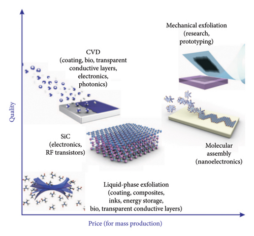
So far, the market of graphene applications is essentially driven by progress in the production of graphene with properties appropriate for the specific application, and this situation is likely to continue for the next decade or at least until each of graphene’s many potential applications meets its own requirements. The properties of a particular grade of graphene depend very much on the quality of the material, type of defects, substrate, and so forth, which are strongly affected by the production methods as briefly summarized in Figure 4 [86]. This chart helps us understand the relationship between mass production quality and price of different graphene components.
3. Physical Properties of Graphene Materials
3.1. Mechanical Properties
Graphene is currently known as one of the thinnest materials in the world, with excellent flexibility and the ability to bend freely. It is also one of the strongest materials ever proven, about 100 times that of steel. Although graphene has excellent flexibility and strength theoretically, it is relatively brittle and is often used as a dopant for other substances in practice, the mechanical properties of which are influenced by various factors, including defects, the bonding quality between adjacent grain boundaries, and the angle between grain boundaries [87]. Graphene, which exists independently and has very few defects, has an elastic modulus of up to 1 TPa, a fracture strength of 42 N/m, and a tensile strength of 130 GPa under 25% tensile strain conditions [88–91]. Therefore, its high flexibility and high fracture strength make it suitable for applications in flexible materials, curved screens, wearable devices, and other fields. The properties and applications of graphene are summed up in Table 2.
| Performance | Characteristic | Indicators | Application | Ref. |
|---|---|---|---|---|
| Mechanics | High fracture strength | 42 N/m | Mechanical structure | [10, 92–94] |
| High flexibility | Bending does not affect its performance | Flexible materials, curved screens, wearable devices | ||
| Electricity | High electron mobility | 2 × 105 cm2/(V·s) | Chips, integrated circuits, sensors, Li batteries | [95–98] |
| Excellent conductive | 10−6 Ω·cm | Supercapacitors and energy storage components | ||
| High specific surface area | 2630 m2/g | Sensors, catalytic carriers, supercapacitors | ||
| Thermal | Excellent thermal conductivity | 5.3 kW/(m·K) | Heat dissipation and thermal conduction components | [6, 99, 100] |
| Optics | Excellent single-layer absorbance | 2.30% | Transparent conductive thin film | [87, 101–103] |
3.2. Electrical Performance
Graphene is a one-atom-thick carbon allotrope with an unusual 2D Dirac-like electron excitation, and the Dirac electrons can be controlled by applying external electric and magnetic fields, or by changing the geometry and/or topology of the sample. Such Dirac electrons exhibit unusual behavior in tunneling, confinement, and integer quantum Hall effects [97]. The band structure of graphene is shown in Figure 5. Due to the symmetry of the sublattices at positions A and B, the dispersion relationship of 2D electron energy exhibits isotropic characteristics near the K and K′ points in the Brillouin zone [101]. The special band structure of graphene endows itself with many physical and chemical properties that are different from general condensed matter, for instance, the ballistic transport characteristics at the submicron scale at room temperature [104], anomalous quantum Hall effect [105], Anderson weak local variation [106], and nonzero minimum quantum conductivity [107].
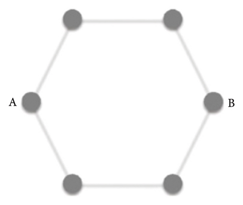
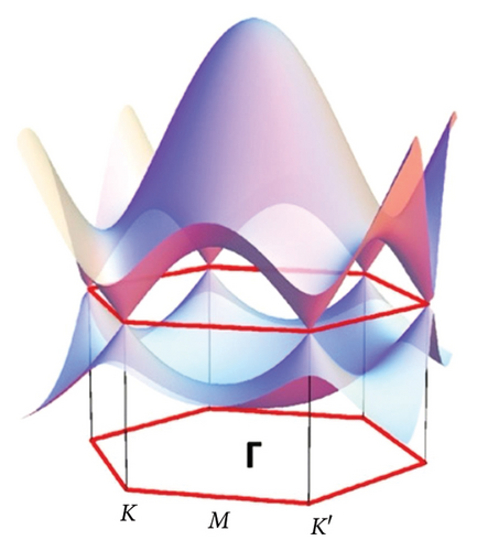
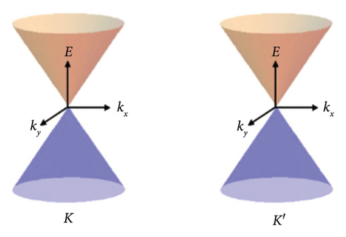
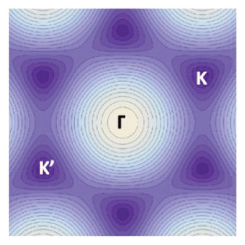
Specifically, the carrier mobility of graphene is about 15,000 cm2/V·s at room temperature, which is more than twice that of the currently highest carrier mobility substance, indium antimonide (InSb). And under certain specific conditions (i.e., low temperature), the carrier mobility of graphene can even reach up to 250,000 cm2/V·s. The possible reason that contributes to a higher carrier mobility could be explained by the fundamental valence state transition. Since the sp2 hybridization of the carbon atom forms a σ-bond in graphene, and the remaining electron on the p-orbital of the carbon atom forms a large π-bond. Thus, in one graphene unit cell, three σ electrons form lower valence states, while the delocalized π and π∗ states form the highest occupied valence state and the lowest unoccupied conduction band [108, 109].
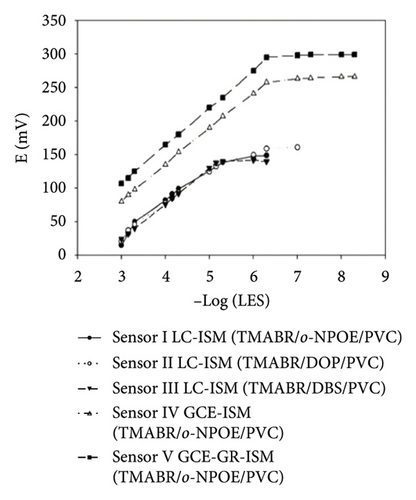
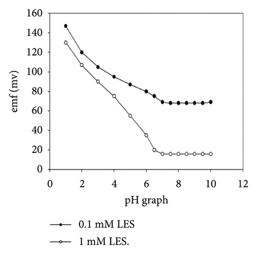
The characteristics of high electron mobility and high specific surface area enable graphene to be applied in varied fields, such as sensors, catalytic carriers, and energy storage components. Namely, a paper-based fully printed electrochemical sensor modified with reduced graphene nanoribbons (rGNR) was developed (Figures 6(a) and 6(b)) [110] with significantly improved sensitivity of detecting antibiotics by adding rGNR. Additionally, an ultra-sensitive sensor that integrates metal–organic frameworks (MOFs) with graphene nanoribbons (Figures 6(c) and 6(d)) [111] was developed for sensing the concentrations of the analyte carbendazim at the level of flying moles (10–15). Besides, an electrochemical sensor using graphene nanomaterials as ion–electron transducers on a glassy carbon electrode (GCE) as the substrate was constructed [112] for selectively determining potential degradation products and impurities in both pure and pharmaceutical formulations of levocetirizine (LES) (Figures 6(e) and 6(f)).
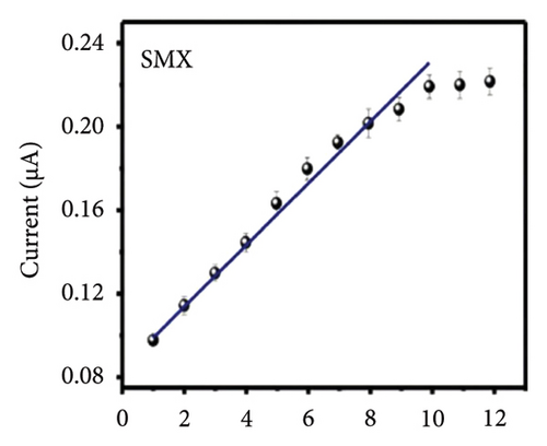
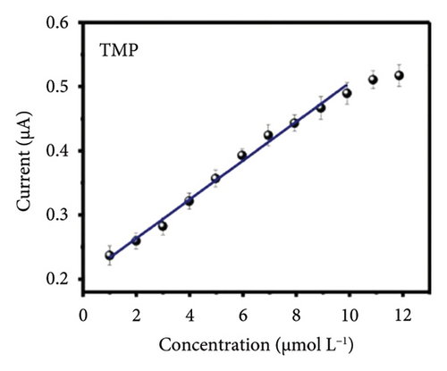
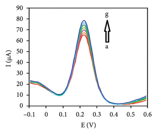
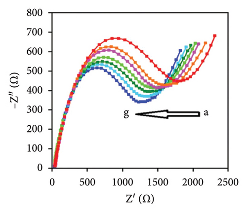
On top of those, the timeline for the development of possible application for graphene-based prototypes is summarized in Figure 6, especially for the display and electronic devices. In Figure 7 [86], display applications achieved by using graphene of medium quality are shown in green till around 2021, while the electronic ones are shown in blue requiring large-area graphene. This figure gives an indication of when a functional device prototype could be expected based on device road maps and the development schedules of industry leaders.

3.3. Thermal Performance
The thermal conductivity and thermal expansion rate of graphene have always been the main research parameters in the field of carbon materials. And the excellent thermal conductivity of graphene comes from the strong binding force of carbon atoms and minimal loss of thermal energy during transmission.
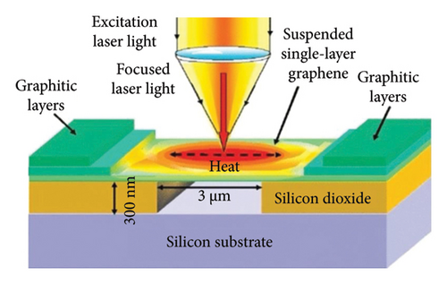
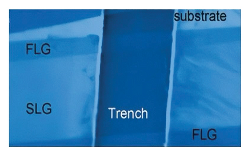
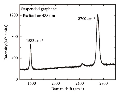
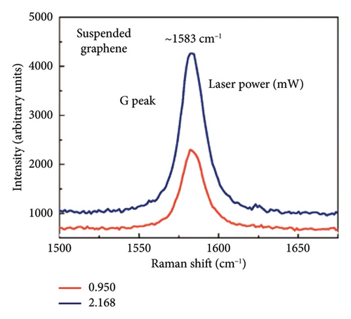
In 2008, researchers used confocal microscopy Raman spectroscopy to measure the heat transfer of suspended graphene nanoribbons and extracted the room temperature thermal conductivity values of SLG, ranging from (4.84 ± 0.44) × 103 to (5.30 ± 0.48) × 103 W/m·K at room temperature [113]. The schematic of the experiment is shown in Figure 8(a) [6], and the scanning electron microscopy (SEM) image in Figure 8(b) gives a close-up view of the suspended graphene layers over the 3-μm-wide trench. Figure 8(c) shows that the suspended graphene flake has the Stokes G peak at 1583 cm−1 and a symmetric 2D band around 2700 cm−1 [6]. The excitation power at the graphene sample location was determined with the power meter. The increase in the excitation power led to the increase in the intensity count and red shift of the G-mode peak. The intensity increase is clearly seen in Figure 8(d) [6].
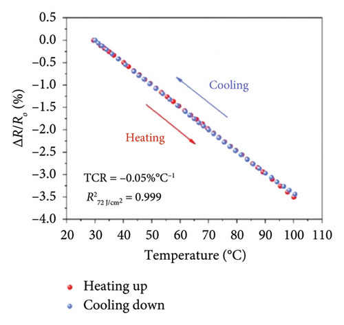
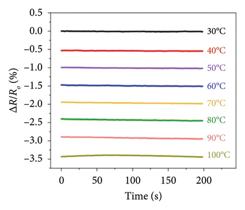
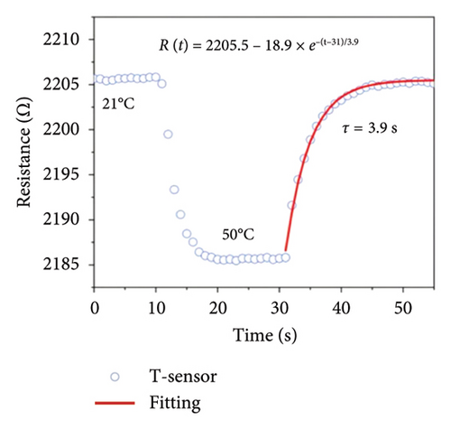
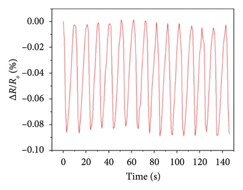
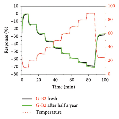
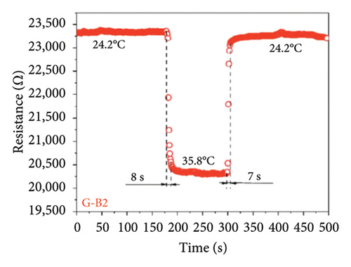
Afterward, some researchers attempted several methods to determine the thermal conductivity of SLG. For example, Zhang et al. [21] proposed a method for the preparation of high-linearity flexible graphene-based temperature sensors by laser writing directly on polyimide (PI) substrates, and the linearity of the temperature sensor was about 0.999 over the temperature of 30°C to 100°C with the laser power density of 76 J/cm2 and the path width of 0.8 mm, while the sensitivity of laser-induced graphene (LIG) sensor is 0.05%/°C (Figure 9(a)), exhibiting a fast response speed within 2 s and a short recovery time in 3.9 s well as the relatively stable resistance throughout all temperature stages over a continuous period of 200 s (Figure 9(b)). Furthermore, the resistance change of the LIG temperature sensor during natural cooling after heating is with a recovery time of only 3.9 s (Figure 9(c)) and excellent repeatability and reliability over 15 cycles, maintaining a fair stable cyclic response (Figure 9(d)). In another word, this graphene temperature sensor has good repeatability, reliability, stability, and flexibility. Šedajová et al. [114] introduced a temperature sensor that utilizes graphene derivatives to mitigate humidity interference, which operates normally within the temperature range of 10°C to 90°C with a resistivity temperature coefficient of 8.63 × 10⁻³ K−1 that is more than twice that of traditional platinum thermometers (Figures 9(e) and 9(f)).
3.4. Optical Performance
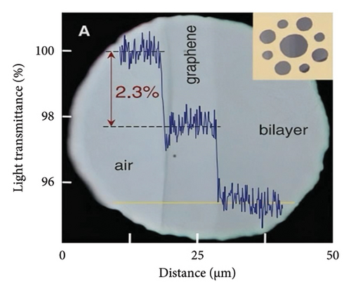
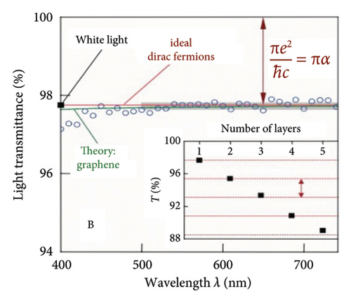
In addition, a theoretical study of graphene by using the tight binding model was presented in 1947 by Wallace [117], which stated that graphene is a zero-gap semiconductor where the valance band and the conduction band touch one another at the Dirac points (K and K′) in the first Brillouin zone. The importance of the Dirac point is that the charge carriers (e.g., electron) in graphene behave like massless Dirac-like elementary particles around the Dirac point. These massless particles follow the relativistic Dirac equation and move with a much-reduced speed of light (c/300) in vacuum. Using Fermi’s golden ratio law to calculate the absorption of light by 2D Dirac fermions, the opacity of graphene is derived as Equation (3) [115]. So far, theoretical studies and experimental measurements (Figure 10(a)) show that the transmittance in the visible light range of single graphene layer is about 97.7% with a difference of 2.3% in transmittance as the number of layers increases and is not affected by the wavelength of the incident light [115], and the opacity of graphene is 2.3 ± 0.1% with a low reflectivity (< 0.1%) [115], which also illustrated that the opacity increases by 2.3% for every additional layer of graphene on the membrane [115]. Meanwhile, Figure 10(b) measurements also yield a universal dynamic conductivity G = (1.01 ± 0.04)e2/4ℏ over the visible frequencies’ range (5), that is, the behavior expected for ideal Dirac fermions. Besides, the transparency of graphene can be changed by regulating gate voltage [120], and due to the neutrality of photons, it is difficult to control the light field, which could be regulated by controlling the carrier concentration in graphene [121].
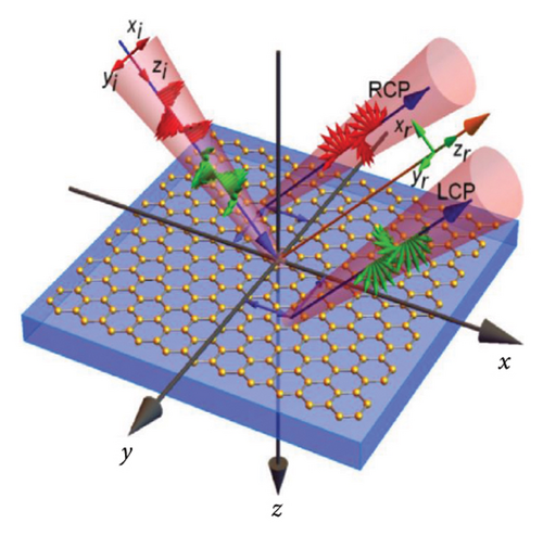
In addition, an electrically tunable optical spatial differentiation technique was developed by introducing graphene layers on quartz substrates [118], providing a potential pathway for expanding more functional optical simulators in the future. A Gaussian wave packet with monochromatic frequency impinging from air to the graphene–quartz substrate interface is shown in Figure 10(c), the z axis of the Cartesian coordinate system (x1, y1, z1) is perpendicular to the interface, and (xi, yi, zi) and (xr, yr, zr) represent the coordinate systems of the incident and reflected beams.
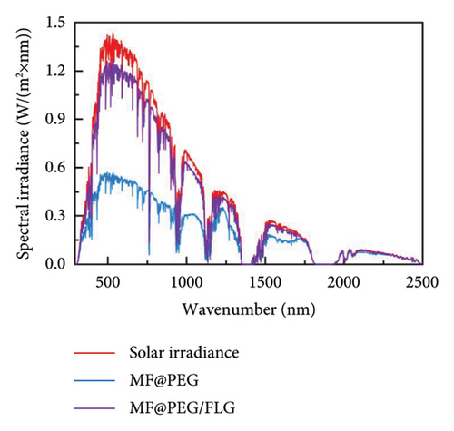
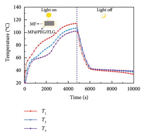
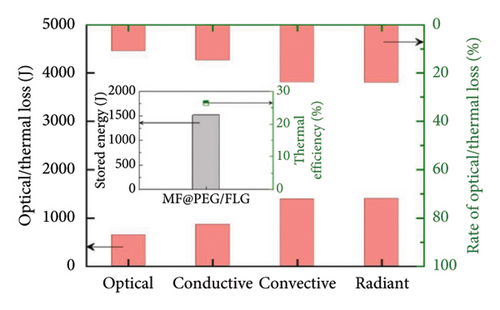
On the other hand, introducing graphene into phase change composite (PCC) materials, the optical losses can be suppressed by 30% while increasing the efficiency of photothermal storage (PTS) by 5.5% [119], offering a fresh perspective for the efficient utilization of solar thermal energy in optical and thermal management. Figure 10(d) compares the solar absorption feature of PCCs. As an improvement, the average absorbance of the FLG-doped PCC is increased by 30% due to the super-conjugated π bonds of FLG, implying the superior light absorption property of the prepared PCCs. As shown in Figure 10(e), the optical loss is 11%, reduced by nearly three times, but the conductive, convective, and radiant thermal losses are increased by 8.4%, 6.9%, and 9.1%, respectively, owing to the increased temperature (Figure 10(f)), and thus, the PTS efficiency of MF@PEG/FLG is only improved by 5.5%. These results signify that the photothermal filler plays a crucial role in enhancing the light absorption properties of the pristine PCC, but the share of thermal losses also increases, resulting in a limited enhancement in PTS efficiency. Therefore, attention should also be paid to suppressing thermal losses.
As a thin carbon material with significant conductivity, graphene plays a crucial role in improving the performance of flexible sensors and makes itself also the most promising material for manufacturing flexible sensors in recent years [122, 123], demonstrating an increasingly excellent performance in the field of sensor integration, which are widely used in medical health, motion detection, fire protection, and other fields.
4. Conclusion
In this review, we conduct a comprehensive analysis of graphene from its preparation to its properties. It is mainly intended to provide a general reference for researchers who are interested in graphene but have not yet delved into this field. From the preparation technology, the mechanical exfoliation method could prepare high-quality and large-size graphene, but quite costly, while the redox method has low cost with inherited defects and impurities in the prepared graphene. Alternatively, CVD can prepare large-area, high-quality graphene, but too costly and difficult to be applied into massive production. Lastly, the epitaxial growth method can prepare graphene with controllable size and high quality, but with clearly disadvantages of harsh conditions, less cost-effective, and low efficiency.
From the structural performance, graphene is a highly versatile 2D material, and its extended honeycomb network is the basic building block of other allotropes, which can be stacked to form three-dimensional graphite, rolled to form one-dimensional nanotubes, and encapsulated to form zero-dimensional fullerenes. Besides, graphene materials exhibit superior properties. These properties include high tensile strength, excellent electrical conductivity, thermal stability, abundant active sites, large specific surface area, low cost, and good biocompatibility. Due to its outstanding properties, graphene-based nanomaterials have very promising research significance and considerable commercial development prospects.
In the future, graphene will have more extensive applications in flexible sensors, ultra-thin displays, new energy, nanorobots, biomedicine, human–computer interaction, and other fields. In summary, the excellent properties and manufacturing technology of graphene were mainly emphasized, and also briefly describe its morphology characterization and latest applications. However, the research and application of graphene materials still face some challenges, such as high preparation costs, complex preparation processes, and the stability and controllability of graphene materials. Therefore, it is necessary and necessary to further research and develop new graphene preparation technologies in the future to improve the performance and stability of graphene materials, and explore their applications in more fields.
Ethics Statement
This research was conducted in a legal and ethical way and is completely in compliance with ethical standards.
Conflicts of Interest
The authors declare no conflicts of interest.
Author Contributions
Writing–original draft, Xue Zhang; writing–review and editing, Xueyu Wu; supervision, Shengbin Cao and Lixia Hu. The authors have accepted responsibility for the entire content of this manuscript and approved its submission.
Funding
No funding was received for this research.
Open Research
Data Availability Statement
The data that support the findings of this study are available on request from the corresponding author. The data are not publicly available due to privacy or ethical restrictions.


