Enhanced Contrast Agent for X-Ray Imaging Using Gold–Silicon Core–Shell Nanostructures
Abstract
Gold nanoparticles (AuNPs) have been targeted as novel contrast agent for computerized tomography (CT). However, AuNPs suffer from low-contrast factor in the X-ray regime. Functionalization of AuNPs with folic acid or sugar-based molecules to induce selective uptake have displayed contrast enhancement with improved image brightness and CT signal intensity. However, it was not clear what the basic mechanism for the contrast enhancement was and whether it was related to the uptake enhancement or to a fundamental electromagnetic interaction effect. In this work, we conducted near-field Mie as well as finite-difference time-domain (FDTD) field distribution of the scattering to discern the effect of a thin dielectric coating layer on the contrast functionality of AuNPs. Our results show that upon the incorporation of the dielectric shell (thin film or nanoparticle layer), the cross section of X-ray scattering is enhanced, with silicon being more effective than silica coating, with multiresonance spectral response. The directionality and range and strength of the near field increase for silicon coating (high electron density or high k material in the visible). The effect may be understood in terms of several features. Even though the refractive indices of all materials in the X-ray regime are ∼ 1.0, the wavelength dependence of their approach may exhibit sizeable differences The enhancement is understood in terms of high densities of polarization charge especially in silicon, which allows multipole resonances. The multiplicity of resonances leads to enhanced scattering and directionality (angular distribution) with reduced range. A silicon-coating layer on AuNP may not only alleviate the contrast limitation, but it may afford synergistic integration of luminescence and scattering functionalities in the visible and X-ray regimes.
1. Introduction
Computerized tomography (CT) uses a combination of X-rays and computer technology as a diagnostic procedure to produce images of the inside of the body [1, 2]. In standard X-ray diagnostics [2], the body part being studied is bombarded by an X-ray beam, with the variations of the energy of the beam after it passes through skin, bone, muscle, and other tissues that are recorded by a plate placed behind the body part. In CT technology, computer software makes three-dimensional images possible, which provide a lot more details about internal organs and other structures than the standard version, including the bones, muscles, fat, organs, blood vessels, internal bleeding, internal injuries or damage, tumors, and tissue or fluid biopsy. Further investigations during the last decade have demonstrated that CT imaging can be improved by the incorporation of X-ray contrast agents, which afford both anatomical and functional data. The use of contrast agents is intended to improve the ability to find any abnormalities and to afford better observation and resolution of the organ or tissue under study. However, this advancement has not gained widespread clinical use because of the limitations of contrast agents. The used contrast agent is iodine-based compounds [3, 4]. A popular compound that is used in CT scans and myelography is iohexol, which is iodine-based, water-soluble organic compound that enhances internal organs during imaging scans. They are radiopaque, meaning that they absorb X-rays and make nonbony tissues and blood vessels appear more distinct. However, they suffer from several drawbacks including high osmolality and short blood half-life, limited contrast due to moderate atomic number (Z), lack of tumor-specific targeting ability, and difficulty of delivery to disease sites at a concentration detectable by current CT scanners.
Recent nanotechnology advances have allowed the development of novel classes of contrast agents, including gold nanoparticles (AuNPs) [5–8]. AuNP offers advantages over iodine compounds due to its size, atomic number, surface-area-to-volume ratio, and larger molecular weight. However, AuNPs suffer from low-contrast factors in the X-ray regime. X-rays, a form of light with a wavelength in the range of 0.01 to 10 nm, correspond to the range of 3 × 10¹⁶–3 × 10¹⁹ Hz, or 100 eV to 100 keV, much higher photon energy than visible light and UV rays. When AuNPs were coated/functionalized by folic acid [9, 10] or sugar-based molecules [11–14] to increase selective uptake, an increase in image brightness and CT signal intensity was observed in cells. Many functionalization methods were introduced [15–21]. It is not clear however what the basic mechanism for the contrast enhancement was and whether it was related to the uptake enhancement or radiation dose variation or to a fundamental electromagnetic interaction effect. We conducted detailed Mie scattering theory [22–25] and finite-difference time-domain (FDTD) analysis [26–28] of Maxwell equations to evaluate the prospect of electromagnetic effects due to dielectric/semiconductor thin layer on the contrast functionality of AuNPs. We examine the total scattering cross section, and the angular field distribution by bare and coated gold for a range of sizes and compositions and incident wavelengths. The dielectric shell coating can be a thin 1- to 3-nm nanofilm or intrinsic nanoparticle layer (in a core–shell architecture). The scattering response is examined for silicon as well as silica material. Although the dielectric constant in the X-ray regime is near 1.0 for all materials, the rate and spectral range where it approaches or dips below that of vacuum (1.0) as well as the degree of dipping depend on some characteristics of the material. Those variations may be the cause of the enhancements of scattering and contrast and that could sharpen/focus scattering directionality in the forward direction and provide synergistic integration of luminescence and scattering functionalities, covering both visible and X-ray regimes.
2. Theoretical Analysis
2.1. Optical Characteristics in the X-Ray Regime
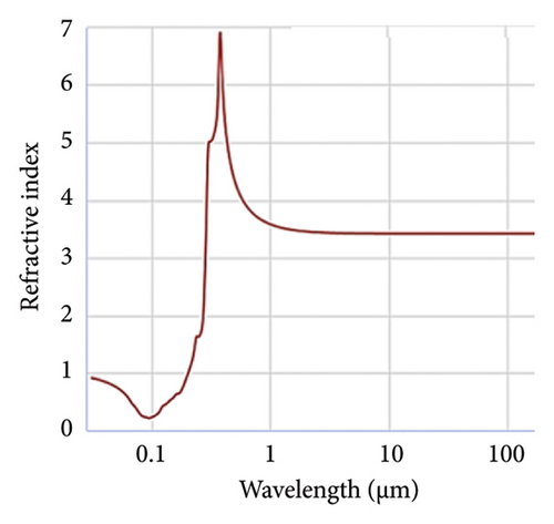
X-rays interact rather weakly with matter (e.g., absorption lengths are on the order of millimeters). Hence, X-ray refractive indices are extremely close to or below 1.0 (that of vacuum). Figure 1 gives the refractive index of silicon crystal as a function of wavelength from the infrared to extreme UV at 30 nm [29, 31]. It exhibits three peaks at 3.5, 4.6, and 5.5 eV which are referred to as E1, E2, and E3 [30, 32, 33]. The E1 (3.4 eV) generally corresponds to transitions between the valence band maximum and the edge of the conduction band minimum at the gamma point (the center of the Brillouin zone), while the E2 (4.4 eV) and E3 (5.3 eV) involve transitions between the valence band and higher complex band extrema. These exhibit strong optical responses and contribute significantly to the absorption and reflectance spectra of silicon. The figure shows that, for shorter and shorter wavelengths, the real refractive index approaches 1.0 (characteristic of vacuum) and begins to dip below it at 197 nm incident wavelength, reaching as deep as 0.24 at 100 nm, then rising back asymptotically to 1.0 (reaching 0.92 at 30 nm). Having a maximum dip of 0.76 below the vacuum makes silicon one of the most responsive materials. In the region below 1.0, one can write the complex refractive index as n = 1 − δ + iβ, where δ is the refractive index decrement and β is the absorption index [34, 35]. The real part of the refractive index (1 − δ) describes the phase shift of the X-rays, while the imaginary part (β) describes the attenuation (or absorption). Theoretical analysis shows that the decrement can be written as δ = (ρereλ2)/(2π), where ρe is the total electron density of the material and λ is the wavelength of te incident radiation and inversely proportional to re the classical electron radius, a fundamental constant, equal ∼ 2.818 × 10⁻¹⁵ m. Below 30 nm in the soft to hard x-ray regime (100 eV to 10 keV), the decrement continues to rise asymptotically but may not be fully smooth to 1.0 (δ decreases) as shown in the inset (lower right).
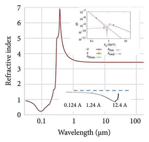
For even higher photon energies in the gamma regime [36], the expression for δ is the same as in the X-ray or EUV. The newly measured index of refraction (|δ|) in the γ regime for γ energies in the range 0.1 to 10 MeV (shown in the inset upper tight) exhibits the same dependencies as X-rays. The decrement dip δ continues to drop and asymptotically reaches 1.0, but it also runs into a local resonance at ∼ 0.9 MeV, and it reverses the sign by crossing 1.0. In this MeV range, additional quantum mechanical effects are exhibited above and beyond the X-ray response. The blue dashed curve shows the negative δ from the virtual photo effect, which is confirmed by the measured values for lower γ energies [36]. For the positive δ, virtual pair creation occurs. Also, the superposition of the two δ contributions is shown in the inset.
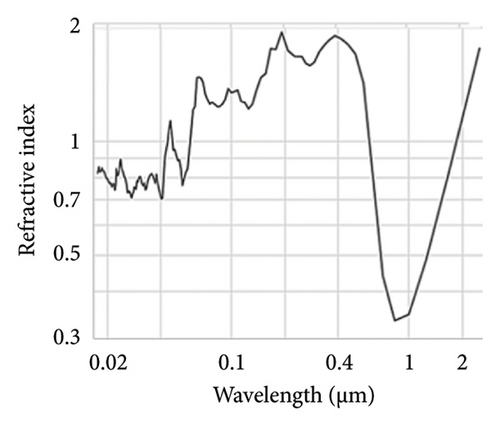
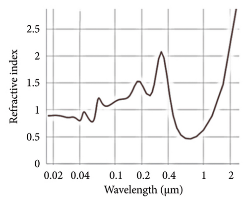
The dependence of the refractive index on the material can be easily seen in Figures 2(a), 2(b), 2(c), 2(d), which give the refractive index n for gold [39, 40] (two figures) and silica [37, 38, 41], in addition to that of silicon [29, 31] in the same photoenergy, respectively. It is to be noted that there is a lack of accurate measurements, and data are lacking over the entire X-ray range. Although at wavelengths < 50 nm, all materials have indices of refraction ≈ 1.0, the approach and the wavelength where it dips below 1.0 depend on the material composition. The X-ray refractive index is influenced by the atomic number (Z) of the material. Generally, materials with higher Z values exhibit stronger X-ray scattering, leading to a greater change in the refractive index. However, the relationship is not strictly monotonic due to resonant absorption edges. In plasmonic materials (e.g., gold), the refractive index is not as smooth as dielectric or semiconductor dielectric material. Figures 2(b), 2(c) show that the refractive index n of gold dips below 1.0 more than once, perhaps due to its oscillatory nature resulting from plasma electronic oscillations in the metal. It dips below 1.0 in the infrared/visible region (0.7–2), in addition to the dip in the region of interest, namely, EUV and X-ray regions. It effectively dips below 1.0 at wavelength of 60 nm, but briefly rises above 1.0 at and then stays down through the hard X-ray regime. In plasmonic materials (e.g., gold), with surface plasmon resonance exhibiting strong optical resonances that can be tuned by changing the material’s shape or surrounding environment, especially dielectric materials of high refractive index (high-k bulk material on the visible like silicon for example) can exhibit Mie resonances, leading to strong enhancement of electromagnetic fields within the material. Figure 2(d) on the other hand is the refractive index of silica whose refractive index dips late below 1.0 at 0.6 nm due to its high band gap (9.1 eV).
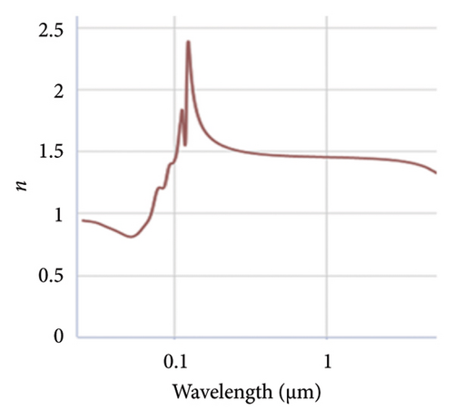
In the photoenergy or wavelength regime and higher intensities we consider in this paper (5–100 nm), we believe the above quantum effects would not play significant roles. At these wavelengths, the photoenergies will not be sufficient to produce virtual electron–positron pairs, nor virtual photoelectrons as would be in the few MeV gamma-ray regimes [36]. Other effects like stochastic effects would be minimized at higher incident intensity. Compton scattering, where photons interact with electrons, and Delbrück scattering, where photons interact with the nucleus, potentially produce electron–positron pairs. The effect was observed at the photon energy of 2.754 MeV [42], which in the soft/EUV conditions would be insignificant.
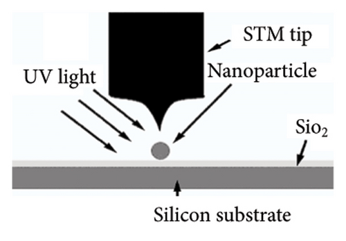
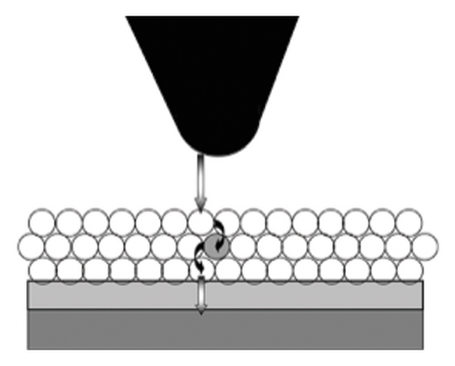
Other quantum effects that must be considered are due to quantum confinement in nanoparticles. In those particles, electrons are subject to quantum confinement and quantum wave reflection/interference off their boundaries, which create discrete energy levels, and hence, electron oscillations are restricted to those electrons within these discrete energy states. Moreover, such confinement leads to enhanced e-e correlation with diminishment of e-phonon interaction which leads to enhanced multielectron excitation by a single photon [43, 44]. Those effects are expected to be stronger under very strong confinement in ultrasmall nanoparticles ≤ 1.0 nm across. We neglect those effects in the present studies as we consider particles or films ≥ 3.0 nm. Moreover, on the ultrasmall limit with a small number of atoms, polarizability is a more appropriate term; nevertheless, the dielectric constant for ultrasmall sizes has been used in the literature. The dielectric constants of ultrasmall Si particles were examined by placing the particles on a silicon substrate, and a scanning tunneling microscope (STM) was used to measure the charging energy of different-sized particles (from I-V spectrum). The measured dielectric constant k and the results from Penn Model and pseudopotential calculations [45] are presented in Figure 3(a), while Figure 3(b) shows the layout of the measurements of a single particle (with allowance of spectroscopy using external light irradiation). In the case of a closely packed thin film (Figure 3(c)), corrections due to the silicon interface as well as the vacuum interface were estimated. The Si substrate typically increases the capacitance by less than 10 percent, only serving to lower the charging energy and therefore will not increase the largest charging energy barrier. For particles protruding above the vacuum interface, the capacitance decreases, hence increasing the largest charging energy. Since we get consistent values from sample-to-sample for each size and a consistent trend with size, the correction is negligible if any. Measured k as function of particle diameter shows that all particles with the exception of the 2.9 nm have values below the bulk value of 11.9.
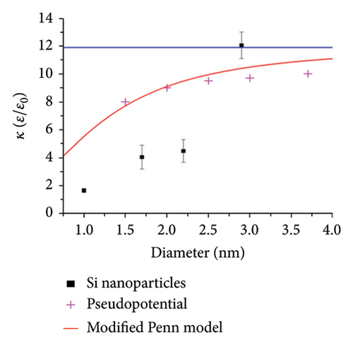
The trend of the measurement shows that for the ultrasmall particle regime, the refractive index drops toward the vacuum value as the size of the nanostructure drops; thus, it is most probably that for X-rays, materials of all sizes will have a refractive index near 1.0. It is generally true that at wavelengths less than 50 nm (EUV), the refractive indices of materials are close to 1.0 regardless of their dimension. To avoid any prospectus effects, we will not use a thickness of 1 nm only in this paper. We will use 1, 3, 12, and 24 nm to allow comparison and evaluation.
2.2. Mie Scattering
We examine the effect of a dielectric semiconductor coating layer on the X-ray/EUV scattering response of a plasmonic AuNP (core–shell architecture). We theoretically analyze the plasmonic and polarizmon dielectric effects involved by conducting Mie-type scattering [22–25] studies as well as FDTD analysis [26–28] of the field distribution of X-ray scattering. We examined individual bare AuNPs and compared it to the response of coated AuNP with a thin dielectric/semiconductor material including closely packed clusters of luminescent 3-nm silicon particles. Mie studies involve the direct analytical solutions of Maxwell’s equations of particles in the presence of electromagnetic fields E and B using series expansions of the involved fields into partial waves of different spherical symmetries to model the interaction of metal–semiconductor nanoparticles with electromagnetic radiation.
We focus on the scattering of X-ray/EUV in the wavelength range 5–200 nm of a bare gold antiparticle as well as concentric core–shell structure of gold and silicon material. Table 1 gives the results for a bare gold particle of 10 nm diameter and 10-nm AuNPs with a dielectric coating consisting of an ultrathin layer of 3-nm-thick silicon. The table gives the real refractive index for both materials (silicon and gold), extracted from Figure 1 at selected wavelengths in X-ray/EUV range. The figure and table show that the materials begin to dip below 1.0 at 197 for silicon and 70 at nm for gold. Note that silicon exhibits one of the largest dips below vacuum (0.76) among materials, whereas gold, for example, dips only by a value of 0.22. The refractive indices exhibit variation with a wavelength that is not monotonic, exhibiting gold local global dips with oscillatory behavior. One notices that the dips in the two materials are not synchronous resulting in large refractive differences that change in sign. Since one expects the scattering of core–shell architecture that depends on the relative refractive index, the effect may not be straightforward to predict, making it more difficult to discern, with dependence on density, atomic weight, atomic number, and anomalous scattering factors of the materials. All materials have a refractive index near one in the X-ray regime. However, the effect of differences caused by those dependencies becomes significant in the approach of 1.0. The results show that the cross section of the Mie scattering for both structures is less than the geometrical cross section (78.5 and 201 nm2 for the bare and the core–shell structures), which indicates as expected that the Mie scattering is weak in this range. Second, the coated AuNP, having an ultrathin coating of 3 nm silicon, shows an enhancement over the bare case, with σ core/σ bare showing an enhancement for most wavelengths. The enhancement reaches as large as an order of magnitude, especially in the soft X-ray/EUV case.
| Wavelength (nm) | Ref. index (Si, Au) | σ core (10 bare) nm nm2 | σ core–shell (10, 3) nm nm2 | σ core/σ bare |
|---|---|---|---|---|
| 210 | 1.126, 1.719 | 0.0017 | 0.0037 | 2 |
| 200 | 0.994, 1.81 | 0.00157 | 0.002 | 1.27 |
| 195 | 0.931, 1.88 | 0.0312 | 0.02 | 0.6 |
| 190 | 0.870, 1.92 | 0.036 | 0.001 | 0.003 |
| 180 | 0.748, 1.78 | 0.036 | 0.0174 | 0.48 |
| 170 | 0.658, 1.75 | 0.042 | 0.074 | 1.75 |
| 160 | 0.639, 1.62 | 0.04 | 0.126 | 3 |
| 150 | 0.576, 1.49 | 0.032 | 0.3 | 10 |
| 140 | 0.525, 1.39 | 0.028 | 0.54 | 20 |
| 120 | 0.406, 1.25 | 0.002 | 1.75 | 875 |
| 100 | 0.241, 1.34 | 0.078 | 5.6 | 72 |
| 80 | 0.276, 1.25 | 0.1 | 10.7 | 107 |
| 60 | 0.620, 1.16 | 0.49 | 7.25 | 15 |
| 40 | 0.852, 0.708 | 2.6 | 14.25 | 5.5 |
| 30 | 0.917, 0.8 | 0.36 | 13.1 | 36 |
| 20 | 0.976, 0.856 | 6.38 | 14.8 | 2.3 |
| 10 | 0.9998, 0.949 | 10 | 19.2 | 1.9 |
| 5 | 0.994, 0.993 | 6.3 | 51.7 | 8.2 |
We examined the effect of the size of the gold core on the scattering cross section keeping the thickness of the silicon cap constant at 3 nm. Table 2 gives the Mie scattering of 10- and 5-nm-diameter AuNPs with 3-nm-thick silicon caps in the spectral range of 5–200 nm wavelength.
| Wavelength (nm) | Ref. index (Si, Au) | σ core–shell (10, 3) nm nm2 | σ core–shell (5, 3) nm nm2 |
|---|---|---|---|
| 210 | 1.126, 1.719 | 33 | 4.1 |
| 200 | 0.994,1.81 | 28.6 | 3.5 |
| 195 | 0.931, 1.88 | 0.01 | 0.2 |
| 190 | 0.870, 1.92 | 0.026 | 0.03 |
| 180 | 0.748, 1.78 | 0.008 | 0.01 |
| 170 | 0.658, 1.75 | 0.17 | 0.02 |
| 160 | 0.639, 1.62 | 0.24 | 0.04 |
| 150 | 0.576, 1.49 | 0.4 | 0.057 |
| 140 | 0.525, 1.39 | 0.66 | 0.08 |
| 120 | 0.406, 1.25 | 1.75 | 0.24 |
| 100 | 0.241, 1.34 | 5.6 | 0.73 |
| 80 | 0.276, 1.25 | 10.7 | 1.52 |
| 60 | 0.620, 1.16 | 8.25 | 1.63 |
| 46.26 | 0.7947, 0.9991 | 6.7 | 1.3 |
| 40 | 0.852, 0.708 | 6.25 | 1.5 |
| 30 | 0.917, 0.8 | 5.1 | 1.68 |
| 20 | 0.976, 0.856 | 14.8 | 2.56 |
| 10 | 0.9998, 0.949 | 19.2 | 10.4 |
| 5 | 0.994, 0.993 | 51.7 | 10.6 |
As expected, the scattering grows with the size of the scattering structure. The table shows that increasing the size of the core size increases the scattering cross section. However, the increase in the core size is bound to increase the size of the silicon shell which also contributes to the increase.
Table 3 gives the effect of the thickness of the silicon capping of AuNPs, keeping the gold core at a diameter of 5 nm. The table details the X-ray scattering cross section for the thickness cases of 3, 12, and 24 nm, respectively. As the thickness of the silicon cap rises from 3 to 12 to 24 nm, the scattering rises in the cross section. For 40 nm wavelength, it rises from 1.3 to 139, to 1620 nm2.
| Wavelength (nm) | Ref. index (Si, Au) | σ core–shell (5, 3) nm nm2 | σ core–shell (5, 12) nm nm2 | σ core–shell (5, 24) nm nm2 |
|---|---|---|---|---|
| 210 | 1.126, 1.719 | 4.1 | 4.5 | 4.4 |
| 200 | 0.994, 1.81 | 3.5 | 0.004 | 1.2 |
| 195 | 0.931, 1.88 | 0.2 | 0.3 | 10.5 |
| 190 | 0.870, 1.92 | 0.03 | 1 | 29 |
| 180 | 0.748, 1.78 | 0.01 | 3.9 | 101 |
| 170 | 0.658, 1.75 | 0.02 | 7.6 | 232 |
| 160 | 0.639, 1.62 | 0.04 | 10.6 | 252 |
| 150 | 0.576, 1.49 | 0.057 | 21 | 374 |
| 140 | 0.525, 1.39 | 0.08 | 26.3 | 534 |
| 120 | 0.406, 1.25 | 0.24 | 60 | 1050 |
| 100 | 0.241, 1.34 | 0.73 | 137 | 1870 |
| 80 | 0.276, 1.25 | 1.52 | 227 | 2620 |
| 60 | 0.620, 1.16 | 1.63 | 212 | 2400 |
| 40 | 0.852, 0.708 | 1.3 | 139 | 1620 |
| 30 | 0.917, 0.8 | 1.5 | 102 | 1420 |
| 20 | 0.976, 0.856 | 1.68 | 69 | 762 |
| 10 | 0.9998, 0.949 | 2.56 | 92.4 | 670 |
| 5 | 0.994, 0.993 | 10.4 | 276 | 819 |
Finally, we examine the effect of the gold core on the Mie scattering. We replace the AuNP with a vacuum core, which results in a silicon bubble. We calculated the scattering results for a vacuum core for a silicon thickness of 12 nm. The results show essentially very little effects of the gold part. Table 4 gives the case of 12 nm thickness as an example, showing that the gold nanostructure is essentially a “passive” substrate that holds the thin dielectric silicon layer. The trend indicates that dielectric layer coatings dominate the scattering of X-rays. The gold nanostructure essentially acts as a “passive” substrate to hold the thin dielectric silicon layer.
| Wavelength (nm) | Ref. index (Si, Au) | σ core–shell (5, 12) nm Au n from calculator nm2 |
σ core–shell (5 Au, 12 Si) nm Both n values from the table nm2 |
σ core–shell (5 vacuum, 12 Si) nm nm2 |
|---|---|---|---|---|
| 210 | 1.126, 1.719 | 4.5 | 0.26 | 0.25 |
| 200 | 0.994, 1.81 | 0.004 | 0.035 | 0.0043 |
| 195 | 0.931, 1.88 | 0.3 | 0.33 | 0.35 |
| 190 | 0.870, 1.92 | 1 | 1 | 1 |
| 180 | 0.748, 1.78 | 3.9 | 3.7 | 3.9 |
| 170 | 0.658, 1.75 | 7.6 | 8 | 7.5 |
| 160 | 0.639, 1.62 | 10.6 | 10.8 | 10.7 |
| 150 | 0.576, 1.49 | 21 | 17.4 | 17.5 |
| 140 | 0.525, 1.39 | 26.3 | 26 | 25.7 |
| 120 | 0.406, 1.25 | 60 | 60 | 60 |
| 100 | 0.241, 1.34 | 137 | 133 | 138 |
| 80 | 0.276, 1.25 | 227 | 238 | 237 |
| 60 | 0.620, 1.16 | 212 | 213 | 216 |
| 40 | 0.852, 0.708 | 139 | 128 | 131 |
| 30 | 0.917, 0.8 | 102 | 112 | 109 |
| 20 | 0.976, 0.856 | 69 | 69 | 66.7 |
| 10 | 0.9998, 0.949 | 92.4 | 92.4 | 90.3 |
| 5 | 0.994, 0.993 | 276 | 276 | 275 |
The real refractive index n of silica (SiO2) at longer wavelengths (e.g., 500 nm), is around 1.464, but at short wavelengths, it is important for understanding its behavior in the X-ray region. Theoretical models using atomic scattering factors of silicon and oxygen provide good agreement with experimental data. We now examine silica as another silicon-based material for coating AuNP. Table 5 gives the EUV/X-ray refractive index of SiO2 and index of gold in the range 210–25 nm wavelength. Note that the interesting range in which the refractive index approaches 1.0 is 40–25 nm. Table 6 gives the Mie scattering of 10-nm-diameter bare AuNP, as well as with a silica cap of 3 nm thickness in the spectral range of 25–40 nm wavelength, showing more than fourfold enhancement.
| Wavelength (nm) | Ref. index (SiO2, Au) |
|---|---|
| 210 | 1.156, 1.719 |
| 200 | 1.568, 1.81 |
| 195 | 1.576, 1.88 |
| 190 | 1.585, 1.92 |
| 180 | 1.608, 1.78 |
| 170 | 1.637, 1.75 |
| 160 | 1.670, 1.62 |
| 150 | 1.737, 1.49 |
| 140 | 1.854, 1.39 |
| 120 | 1.90, 1.25 |
| 100 | 1.459, 1.34 |
| 80 | 1.224, 1.25 |
| 70 | 1.049, 1.37 |
| 60 | 0.897, 1.16 |
| 40 | 0.870, 0.708 |
| 35 | 0.89, 0.815 |
| 30 | 0.926, 0.8 |
| 25 | 0.94, 0.80 |
| Wavelength (nm) | Ref. index (SiO2, Au) | σ core (nm2) | σ gold (nm2) | Ratio/enhancement |
|---|---|---|---|---|
| 40 | 0.86, 0.702 | 13.5 | 2.8 | 4.8 |
| 35 | 0.89, 0.815 | 11.7 | 1.92 | 6 |
| 30 | 0.926, 0.8 | 13.3 | 3.6 | 3.7 |
| 25 | 0.94, 0.80 | 17.9 | 5.9 | 3 |
It should be noted that the coating may also be produced by depositing closely packed H-terminated 1 nm particles [46–53]. Hydrophobic forces in an aqueous environment can be used to form this kind of assembly by driving the particles toward and nucleate on the gold surface. Hydrophobic forces have been used to form colloidal crystals with closely packed particles, The particle distribution of the nanoparticles is expected to be random but reasonably uniform. This provides an interparticle atomic scale gap of 3 Å, with a density of the order 1012–1013/cm2. For a AuNP of 10 nm diameter, a total of ∼360 particles of 1 nm diameter are expected for a single monolayer.
2.3. FDTD Analysis (Scattered Field Distribution)
It is interesting to determine the field distribution, angular distribution, spatial range, and focusing effects of the core–shell nanostructures. We calculate these field distribution effects using the FDTD computations in which a discrete solution to Maxwell’s equations is obtained [22–28]. The method is based on central difference approximations of the spatial and temporal derivatives of the curl equations. We use the software of COMSOL Multi-Physics Software 5.3a AC/DC module electromagnetic waves. In the software, the simulation parameters, e.g., the dimensions of perfectly matched layer (PML) and grid size, are a physics-based mesh, with a max element size 0.35 nm, a min element size 0.000 05 nm, maximum growth rate 1.3, curvature factor 0.3, and resolution of narrow regions 1. For simulating unbounded problems, the method uses a reflectionless absorbing boundary (PML method). Moreover, the procedure can absorb evanescent waves and near fields. The procedure can handle the modeling of very complex geometries by using subcell modeling techniques and local subgrids. Subgrids are embedded within the global grid to locally resolve fine geometric structures without sacrificing the global space/time scale. The applications of subcell models and subgridding methods enhance the efficiency and the accuracy of the FDTD method. We apply FDTD to the core–shell architecture. As to the optical constants used in the calculations, and the wavelength dependence of the refractive index for silicon, silicon and gold are taken from previous data and the associated Figures 1 and 2 [29–34]. Those cover the region of X-ray–EUV region 4–20 nm. For the core metal (Au) nanoparticles, we used the values embedded in the COMSOL software package [40]. It is to be noted that there is lack of accurate measurements of the optical constants in the X-ray/EUV regime, and data are lacking over the entire X-ray range. Although at wavelengths < 50 nm, all materials have indices of refraction ≈ 1.0, the approach and the wavelength where it dips below 1.0 depend on some atonic/electronic characteristics of the material composition.
In the optical configuration, we use a linearly polarized incident beam of amplitude Einc (or background field Eb) with an amplitude of 1.0 V/m. A plane wave source is used with the incident beam propagating along the x direction, and the polarization is along the z direction (see the coordinate system and configuration in Figures 4(a), 4(d), 4(g)). The scattered field is defined as Esca = Etotal − Einc, where Etotal is the total field and Einc is the incident field. This definition is enforced at the boundary between the total and scattered fields by adding in or subtracting out a correction term for the update equations on and next to this boundary.
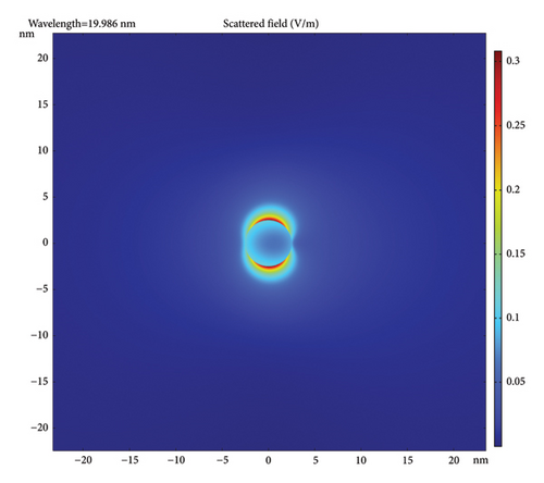
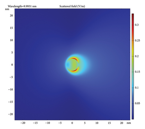
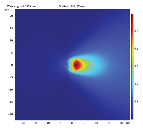

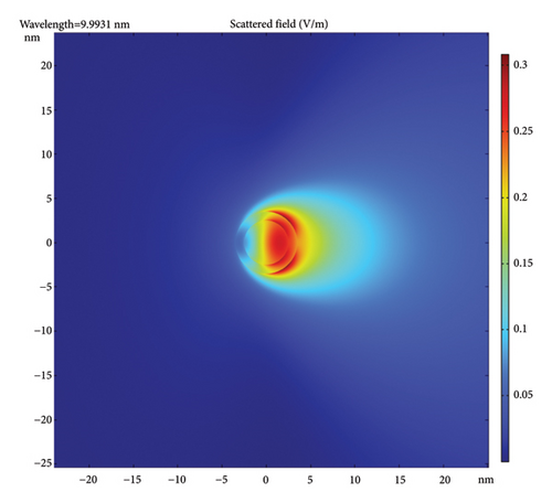
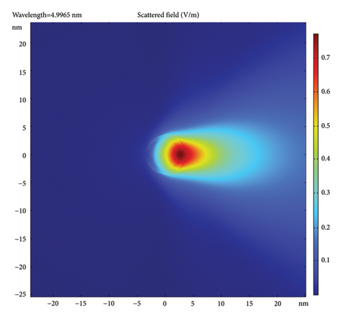
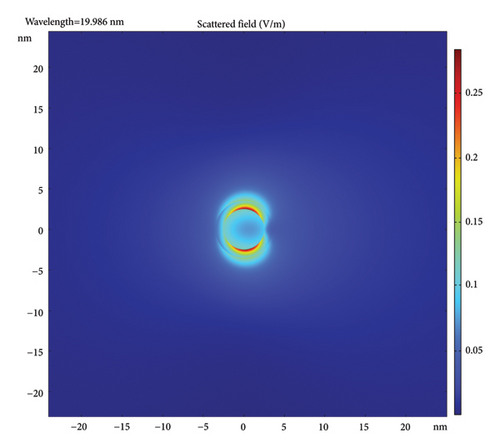
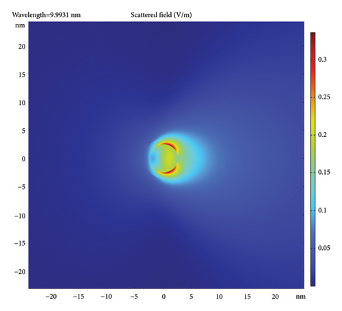
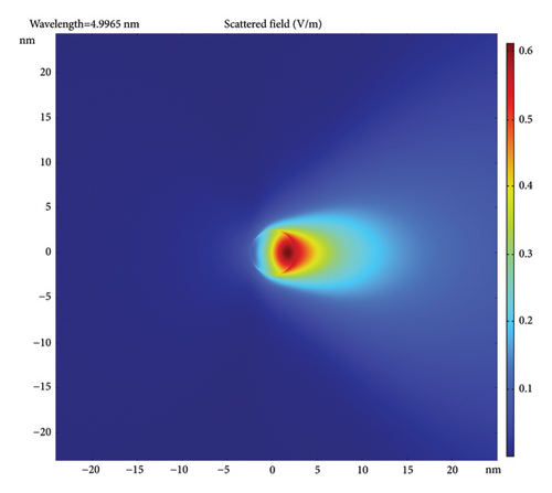
Figure 4 gives the scattered field distributions in the incident plane (plane of propagation and polarization) for the case of 5-nm-diameter AuNPs with different coatings and incident wavelengths. The figure uses a color-coded metric given on the right side of each frame. Note that the color code is different for each but, in all, the dark red is the strongest and the dark blue is the weakest. In all frames, the incident X-ray is a plane wave, incident from the left. The scattered field is normalized to the incident field amplitude of 1 V/cm. Figures 4(a), 4(b), 4(c) show a bare AuNP and 20, 10, and 5 nm incident wavelength, respectively. Figures 4(d), 4(e), 4(f) show a AuNP with 1-nm coating (e.g., silica) and incident wavelength of 20, 10, and 5 nm, respectively. Figures 4(g), 4(h), 4(i) show a AuNP with 1-nm silicon film coating shell and incident wavelength of 20, 10, and 5 nm, respectively. The trend in the frames shows that the scattering is restricted to the forward direction, getting more directional as the wavelength drops. The figure also shows that the scattered polarization/plasmon field is stronger and more focused than the pure plasmonic field, i.e., has a shorter range (shorter effective focal length) with higher intensity. The strongest inner field is more conversing for silicon material coating (a high k-material precursor in the visible).
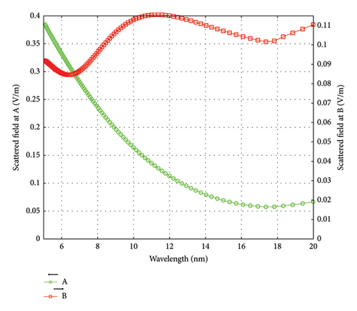
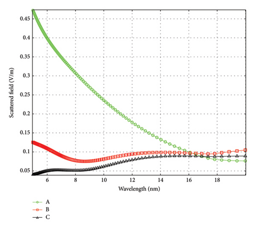
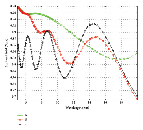
We now compare the scattered intensity at the center and surface of the structure. Figures 5(a), 5(b), 5(c) give as a function of incident wavelength the scattered FDTD electric field for the case of bare 5-nm-diameter AuNPs, and with 1 nm dielectric (silica) with refractive index in the visible of 1.45, but near 1.0 in the X-ray region and with 1-nm silicon-coating shell, respectively (in the visible, the refractive index is 3.5–3.6 but neat 1.0 in the X-ray region). The fields are plotted at points A, B, and C, at the center of the structure and the inner and outer edges of the shell as labeled in the figure. For the pure gold structure, it shows that the scattered field at the center of the nanoparticle is excluded especially at the longer wavelength. The addition of the dielectric coating increases the penetration of the scattered fields inside the structure. Also, it shows the oscillatory as well as the steadiness of the scattered field with wavelength.
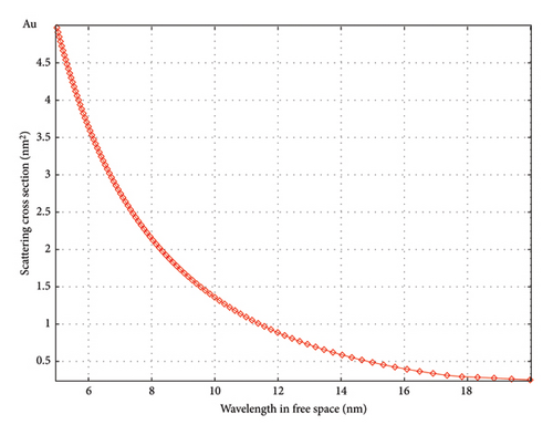
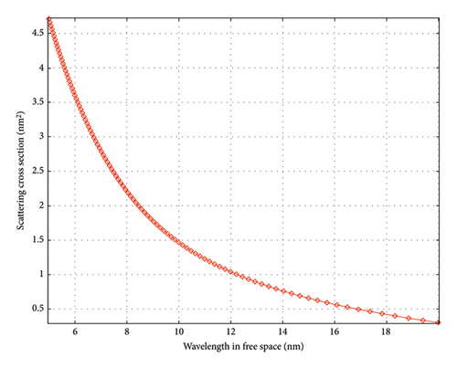
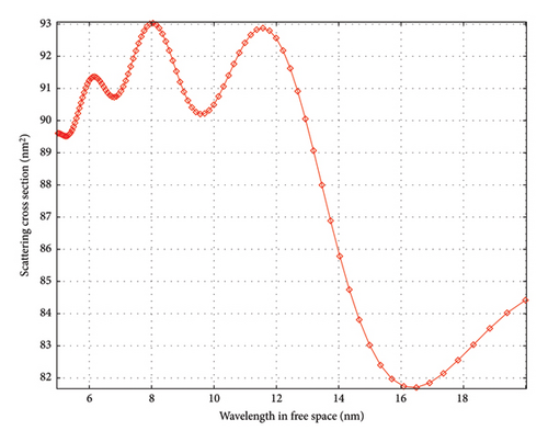
Finally, we examine the total scattering cross section as a function of wavelength. Figures 6(a), 6(b), 6(c) give as a function of incident wavelength the scattered FDTD cross section for the case of 5-nm-diameter AuNPs, for the three cases: bare, with 1 nm silica, and with 1 nm silicon-coating shells, respectively. Figure 6(a) shows that for a bare AuNP, the scattering cross section is structureless over a wavelength range of 5–20 nm, falling from a maximum of 5 nm2 when the incident wavelength matches the diameter of the particle, effectively falling to a level of 0.5 nm2. Wrapping the particles by a silica shell enhances the cross section to 50 nm2, as shown in Figure 6(b), but it remains structureless in this wavelength range while dropping faster to a level of 2 nm2. On the other hand, for a silicon shell (high k material with a refractive index of 3.65 when under visible/UV), the response shows several interesting features (Figure 6(c)). First, it is enhanced to a level of 93 nm2. Second, it remains nearly level over the range 5–13 nm with some residual oscillation with wavelength before it drops sharply at 15 nm to a level of ∼ 80 nm2. The residual ripple is about 3 nm2 peak to peak, with visibility of ∼ 1.5%. However, we should guard that FDTD calculations are sensitive to the input data in the X-ray regime as there is lack or inaccurate optical constants. We should note that lack of accurate measurements and data of the optical constants over the entire X-ray range and that the approach and the wavelength where the refractive index dips below 1.0 depend on the material composition. Moreover, the scattering results for using a different software (e.g., ANSYS Lumerical photonic solver) may give different scattering intensities even for the same input date, let alone with input refractive index from a different source. For example, bare AuNP ANSYS may give results like the COMSOL package (except scattering intensity). Moreover, for gold-coated silicon, both may exhibit Mie-type resonances; however, the spectral responses of shell-coated nanoparticles may differ in shape, position, and magnitude. This strong dependence on the used material data/models does not allow unconditionally trusting numerical simulation results without appropriate experimental confirmation. Therefore, exact numerical results might be suspect, but several trends and features can be less suspect for a given software/input data, such as the prospect of contrast enhancement, multiresonance response, stronger focusing, and near-field range, which can be useful for the development of novel testing.
3. Discussion
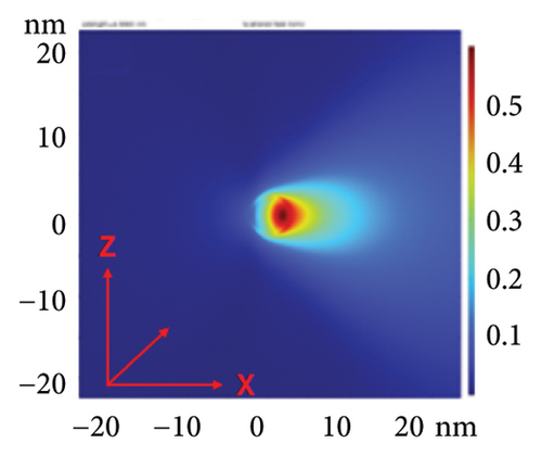
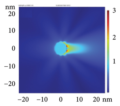
The present results showed that X-ray scattering by AuNPs exhibits an order of magnitude enhancement in the cross section accompanied with multiresonance wideband spectra upon the incorporation of a Si shell (1–3 nm film or particle layer) in core–shell architectures. The enhancement in the cross section and spectral width is larger for silicon (high k material in the visibly/UV) than silica (low k material in the visible/UV). Figures 7(a), 7(b), 7(c) give a closeup of the field FDTD distribution of bare gold (control) and with silica and silicon shells of 1 nm thickness, respectively, for 5-nm incident radiation for the shortest wavelength studied (5 nm) for easy comparison of the angular distribution. Using the color code, scattering in the case of a shell shows that the angular distribution follows a similar trend to the cross-sectional enhancement. The inner distribution narrows and becomes positively focusing along the forward direction. Figure 7 also shows that the near-field scattering is a conversing, being the most conversion for the silicon shell than for bare gold or the silica shell cases. The figure shows that the scattered field range for the 1-nm silicon shell is 12 nm from the center of the structure converging at an angle of 16°.

Figures 8(a), 8(b), and 8(c) give the line profile of the scattered field amplitude [5-m gold particle with a silicon shell (1 nm thickness)] along a diameter along the direction of the polarization of the incident field for the three cases of Figures 7(a), 7(b), and 7(c), respectively. For each case, the line profile is generated for three different incident wavelengths 20, 10, and 5 nm. The figure confirms also that the scattered polarization/plasmon field is more and more in the forward direction diminishing in the 90° direction of the denser silicon material as well as for shorter wavelengths.
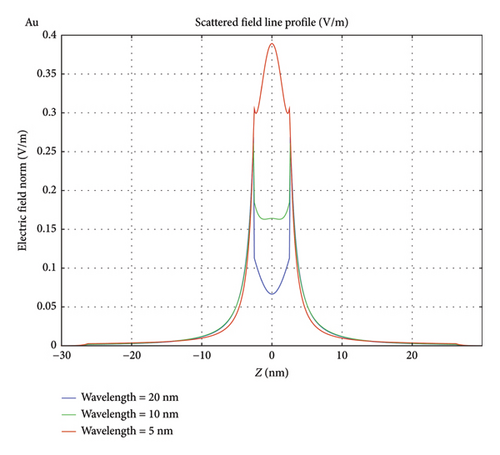
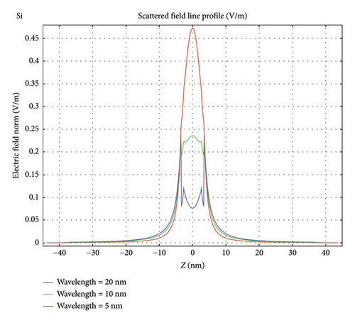
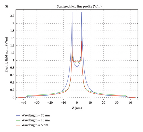
The results are understood in terms of polarization charge [24, 25]. Intrinsic silicon has zero electrons in its conduction band, but it has one of the highest valence charge densities. The density of electrons in the valence band is 1.8 × 10¹⁹/cm3, whereas the density of states in its conduction band is 2.8 × 10¹⁹/cm3, both being more than 3-fold larger than germanium. For comparison, gold has an electron conduction density of 5.9 × 10²²/cm3. The multipole/multiresonance feature response of silicon dielectric affords an opportunity for controlling the overall scattering direction (directionality). Enabling an improvement in the directionality of the scattering is highly useful in enhancing the contrast functionality. The present results show that scattering by plasmonic contrast agents incorporating nonmetallic coatings, such as silicon, is focused on the forward direction, and thus, such structures provide better contrast and resolution than scattering by pure plasmonic metal particles, like gold. Wide angular distribution creates a “noise” effect on the resulting medical image that compromises the contrast and causes heat losses.
It is interesting to mention that recent measurements in which molecular caps were formed on AuNPs for the purpose of enhancing their selective uptake into cancer cells showed also as a side effect some degree of image enhancement. The uptake of cancer cells of bare nanocontrasts is marginal. Glucose-based molecules as well as folic acid molecules were used to functionalize AuNPs to improve the uptake of cancer cell [9–21]. Both FA-modified or glucose-modified AuNP afforded selective enhanced uptake. In vitro experiments demonstrated enhanced uptake and showed that AuNP-DG is internalized and retained in the tumor cells. In addition to improving the uptake, the caps improved the contrast of images. The refractive index of folic acid is based on its chemical structure and solubility, and it is likely to be around 1.5–1.6 in the visible/UV when measured in a suitable solvent like water or ethanol; however, the exact value would depend on the specific solvent and concentration used. Likewise, the refractive index of 2-deoxy-D-glucose in the visible/UV is approximately 1.52. Since 2-deoxy-D-glucose is structurally very similar to glucose, its refractive index in the visible/UV will be close to that of glucose, which is typically around 1.52 in the visible. However, the slight structural difference (missing hydroxyl group at the two positions) could cause a minor variation in the refractive index, but the value in the visible/UV will remain very close to 1.52. It is therefore plausible that our present studies, given above, which demonstrated scattering enhancement may account for the contrast enhancement, seem in these measurements. In fact, it is most probably the measured enhancement may be related to a fundamental interaction EM effect.
Finally, we mention that the present results are useful when considering the issue of safety in CT imaging. While high image quality is an important requirement in CT, the radiation dose must be kept minimal to protect the patients from ionizing radiation-associated risks (safety issue). Enhancement of the contrast functionality will tend to allow a reduction in the intensity of the X-ray used. Thus, in X-ray CT, an optimal compromise between image quality and patient dose must be sought.
It should be noted that the above treatment assumes monochromatic EUV/X-ray. Recent interest is growing on the use of wider width of sources. In fact, recent work on X-ray emission has been focusing on the generation of wideband features [54–56]. Such systems may be useful in increasing the total cross section when broadband X-rays are used for excitation. With wider band excitation, the higher order resonances may be targeted, i.e., the integrated total cross section is the relevant enhancement. It is hoped that nearly another order of magnitude is afforded. A broadband source can provide much higher flux compared with a monochromatic source; however, it conflicts with the necessary coherence requirements of this coherent diffraction imaging technique. Also using a material, such as silicon, in the X-ray regime for imaging is more useful than the use of silica as can be seen from Table 6. Silicon has a wider range of sub-1.0 refractive index, as well as a deeper dip. Those attractive differences may be produced by the higher precursor refractive index and higher electron density. Thus, the optical properties of silicon are almost ideal for a strong X-ray scattering response, as it has a sizable refractive index dip in the X-ray regime (in the visible/UV, it has a refractive index of 3.5–3.6). Note that silicon exhibits one of the largest dips below vacuum (0.76) among materials, whereas gold, for example, dips only by a value of 0.22, while silica by a value of 0.2 (see Figure 2). In addition to their exceptional optical properties, silicon nanostructures are mechanically and thermally exceptional [57, 58].
4. Conclusion
In conclusion, we used Mie theory and FDTD analysis to evaluate the X-ray scattering and field distribution of integrated gold/silicon core–shell nanostructures. The analysis shows significant enhancement of the cross section of X-ray/EUV scattering accompanied by multiresonance wideband spectral response upon the inclusion of a Si shell 1-nm-thick film or particle layer. The results point to an increase in scattering due to the presence of a shell with a large refractive index dip δ, (n = 1 − δ) below 1.0, the characteristic refractive index of vacuum. The results are consistent with previous measurements in which the AuNP used as contrast agents were functionalized/coated with monolayer of glucose or folic acid. With silicon nanoparticles having novel luminescence, and amenability to selective functionalization, the core–shell structure may afford the opportunity for the integration of multiple imaging functionality in the visible and X-ray regimes. The results are understood in terms of scattering off of polarization charge (bound valence charge) in a dielectric; pronounced resonances associated with the excitations of higher modes, in addition to electric dipole and quadrupole distributions, with the multiplicity leading to enhanced response and widened spectral width, which enhance contrast and sharpen scattering directionality (angular distribution), and provide synergistic integration of luminescence and scattering functionalities in cell imaging applications [59, 60].
Conflicts of Interest
The authors declare no conflicts of interest.
Funding
This study was funded by the University of Illinois at Urbana-Champaign.
Open Research
Data Availability Statement
The data that support the findings of this study are available from the corresponding author upon reasonable request.


