Compact Dual-Band Band-Pass Filter Using Single Multimode SIW Cavity With Independent Controllable Fractional Bandwidth
Abstract
This paper introduces a compact dual-band band-pass filter using single multimode (TE101, TE102, TE201, and TE202) substrate-integrated waveguide (SIW) cavity with independent controllable fractional bandwidth (FBW) using metallic vias and slot perturbations. A via is placed at the center of the cavity, to shift the TE101 mode towards the TE102 mode which forms the Passband I with a center frequency (CF) of 16.2 GHz and a FBW of 1.71%. Two vias and slots are positioned and adjusted to shift the TE201 mode and TE202 mode, respectively, to achieve the Passband II with a CF of 19.1 GHz and an FBW of 3.09%. The measured insertion loss (IL) of the proposed filter is 1.8 dB for the Passband I and 1.9 dB for the Passband II.
1. Introduction
Multiband band-pass filters (BPFs) are indispensable components in advanced wireless communication systems, fulfilling the crucial role of managing signals across diverse frequency bands and addressing the intricate challenges posed by modern communication technologies. Various technologies can be employed to implement these filters, each with its own merits and drawbacks. A waveguide with a high Q-factor can handle high power in high-frequency applications. However, their nonplanar structures present integration challenges with planar circuits. Conversely, microstrip filters offer a compact size and ease of integration with other planar circuits. But, their Q-factor typically lags behind that of waveguide. SIW technology strikes a balance between these approaches featuring a planar structure, facilitating seamless integration with other planar circuits. They offer a moderate Q-factor and the ability to handle moderate power levels exhibiting relatively low losses, particularly in high-frequency ranges.
Various methods are proposed for achieving dual-band filters. One approach combines two separately designed BPFs to produce a dual-band passband response [1]. However, the overall size increases. Multi-BPF is achieved through coupling matrix synthesis techniques [2], and this approach is specifically tailored for BPFs with closely spaced adjacent passbands, potentially resulting in larger sizes.
Complementary split-ring resonators (CSRRs) are introduced in the cavity for dual-band frequency response [3–5]. However, it is important to note that such circuits may incur higher insertion losses (ILs). The SIW square cavity was coupled with an E-shaped slot line resonator to achieve a dual passband [6, 7]. Nevertheless, it is crucial to acknowledge that the inclusion of slot lines introduces radiation losses into the structure. Two defected ground structures (DGSs) were incorporated on the above and below surfaces of the SIW cavity to create a dual-band [8]. DGS introduces an increase in IL.
A wideband BPF is obtained using a comb-slotted SIW cavity using a multimode [9]. The dual-band BPF is achieved based on CSRR and multimode cavity [10, 11]. The dual-band BPF is obtained using multilayer dual-mode [12]. Dual-band SIW using cross-coupling via a half-mode BPF [13].
This paper introduces the dual-band BPF design utilizing the SIW cavity’s multimode property. The perturbation of the fundamental mode (TE101) and the next three higher modes (TE102, TE201, and TE202) of the SIW cavity is achieved by placing via-holes where the electric field of TE101 and TE201 is maximum and slots are placed at TE202 where the electric field is minimum. The positions and dimensions of the via-holes and slots are optimized using EM simulations in Ansys HFSS to achieve the desired dual passband response, as briefly explained in the following section.
2. Dual-Band SIW Filter Design
2.1. Filter Specifications
Qe1(Qe1) is the external quality factor, M1(M2) is the coupling coefficients between the modes, and their theoretical values for each passband are Qe1 (33.8), Qe2 (20.8), M1 (0.032), and M2 (0.053), respectively, which are calculated using (1) [14].
2.2. Filter Design
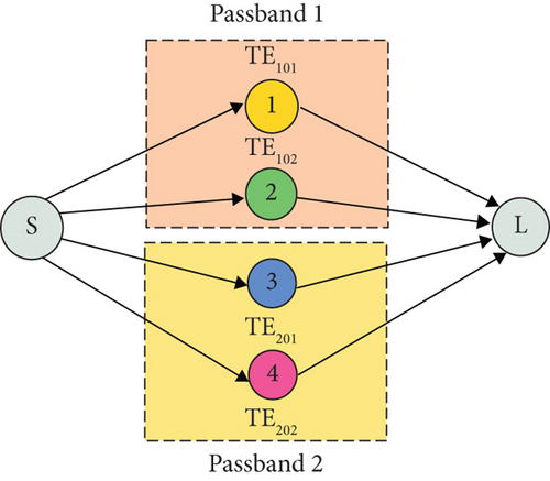
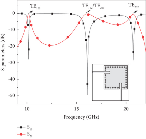
The first four resonating modes in the SIW cavity are considered to achieve second-order dual-band band-pass response. The electric field distribution of the fundamental and higher modes of SIW is presented in Figure 3. The simulated S-parameters of the mutlimode SIW cavity without any perturbation are shown in Figure 4. The resonant frequencies of the fundamental mode TE101 (f1) are observed at 10 GHz, the two degenerate modes TE102 (f2)/TE201 (f3) appear at 16.2 GHz, and a higher-order mode TE202 (f4) occurs at 20.2 GHz.
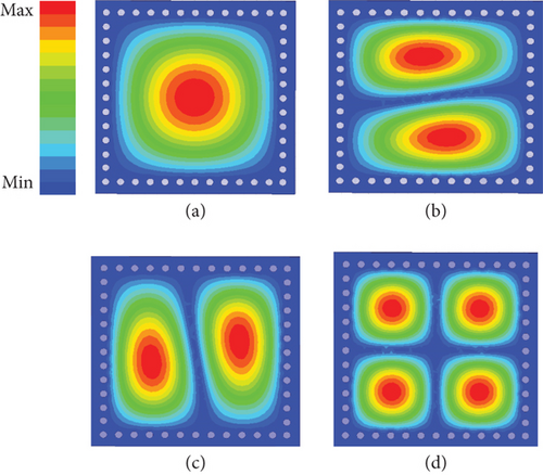
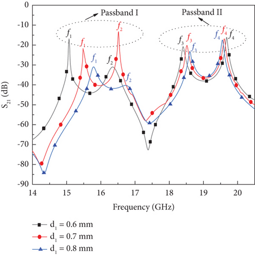
In the proposed design, Passband I is realized by shifting TE101 towards TE102. Similarly, Passband II is realized by shifting TE201 towards TE202. To achieve this initially, via V1 is placed at the center of the cavity, aligning with the maximum electric field position, to effectively perturb the TE101 mode. This placement also slightly affects the TE102 and TE201 modes, due to their minimal electric field distribution at the center. However, since the electric field is nearly zero at the center for the TE202 mode, as illustrated in Figure 3d, via V1 does not cause any significant perturbation. This is further confirmed by the S-parameters shown in Figure 5. By varying the diameter (d1) of via V1 from 0.1 to 0.9 mm, it is observed that the fundamental TE101 mode shifts towards the degenerate TE102 mode, as shown in Figure 5.
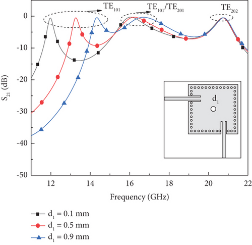
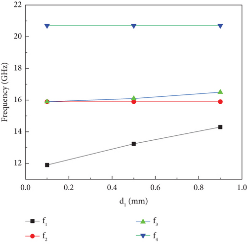
Figure 6 displays the resonant frequencies (f1, f2, f3, and f4) plotted against the diameter of the center via (d1). The variation of d1 from 0.1 to 0.9 mm shows an increase in f1, while f2 and f3 have less effect and no effect on f4. This indicates a significant perturbation on TE101 and minor perturbation of TE102 and TE201 and no effect on TE202.
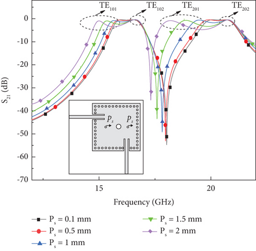
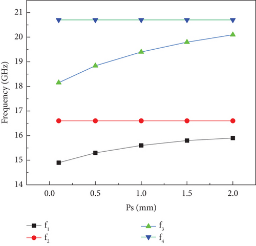
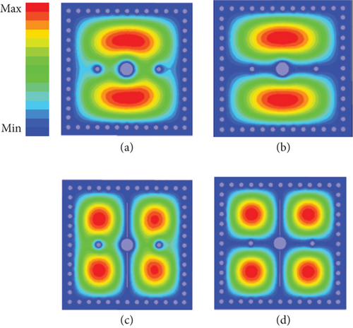
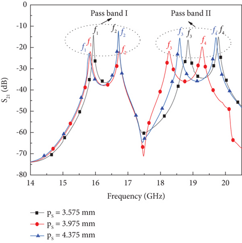
By analyzing the electric field distribution of the resonant modes in Figure 3c, vias V2 and V3 are positioned at the maximum electric field locations (at a distance of PS) to perturb the TE201 mode towards the TE202 mode. As PS increases from 0.1 to 2 mm, as shown in Figures 7 and 8, the TE201 mode shifts towards the higher order TE202 mode, with slight variations in the TE101 mode and no significant effect on the TE102 mode. Hence, the influence of vias V2 and V3 is also taken into account, along with via V1, in shifting the TE101 mode towards the TE102 mode to realize the Passband I. The electric field distributions of the perturbed TE101 and TE102 modes are shown in Figure 9a,b. These modes exhibit similar electric field patterns, ensuring the formation of Passband I.
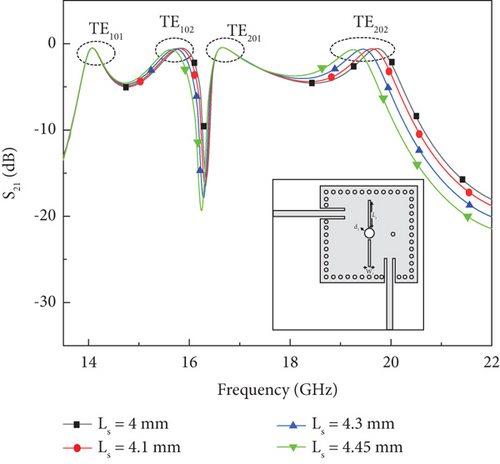
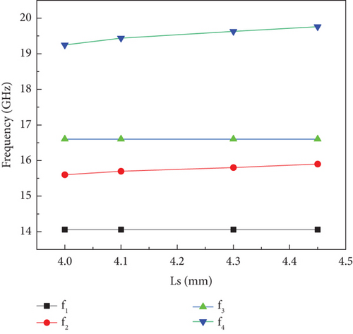
To shift the TE202 mode towards the TE201 mode, a rectangular slot is placed at the location of the minimum electric field in the TE202 mode. When the slot width (WS) is fixed at 0.1 mm and the slot length (LS) is varied from 3 to 4 mm, the TE202 mode shifts closer to the TE201 mode, as illustrated in Figures 10 and 11. Hence, the influence of vias V2 and V3, along with the slots, is considered in perturbing the TE201 and TE202 modes to achieve Passband II.
The electric field distributions of the perturbed TE201 and TE202 modes, shown in Figure 9c,d, exhibit similar electric field patterns, forming the Passband II.
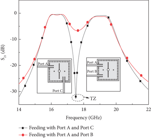
Figure 10 shows a transmission zero (TZ) between the passbands, attributed to the feed alignment, which is carefully designed to enhance isolation between the passbands.
Figure 12 illustrates the electric field distribution of the proposed dual-band filter with the input/output (I/O) feedline arrangements. When Port A and Port B serve as the input and output ports, respectively, the TE201 and TE102 modes exhibit the same electric field polarity, resulting in no TZ between the passbands. However, when Port A and Port C are used as the input and output ports, the TE201 and TE102 modes have opposite electric field polarities, creating a TZ between the passbands due to phase cancellation [16].
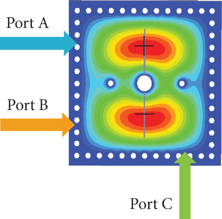
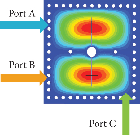
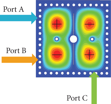
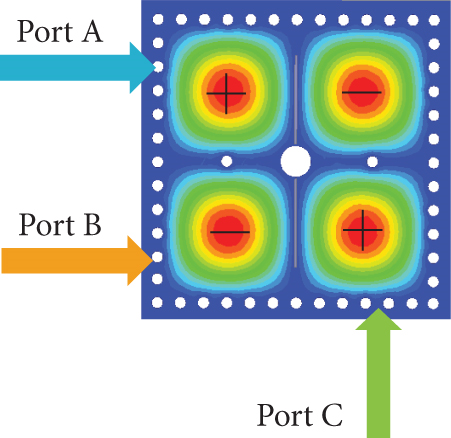
The feedlines are arranged such that the modes of the Passband I (TE101 and TE102) and the Passband II (TE201 and TE202) are out of phase, ensuring high isolation between the two passbands. Therefore, in the proposed design, Port A and Port C are selected as the I/O ports to enhance passband selectivity, with the corresponding response shown in Figure 13.
2.3. Extracting Coupling Coefficients
Figure 14 shows the simulated S-parameters corresponding to the cavity’s first four resonant modes. As the diameter of via V1 increases, the resonant peak f1 shifts towards higher frequencies, thereby affecting the bandwidth of the Passband I. When the diameter of via V1 (d1) is varied from 0.6 to 0.9 mm, the mutual coupling coefficient M1 decreases linearly, as illustrated in Figure 15. The desired FBW for Passband I is achieved when d1 = 0.8 mm.
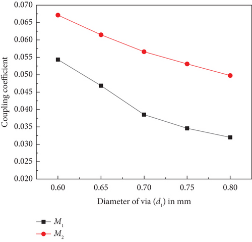
By varying the distance PS, a shift in the resonant frequency f3 towards a higher mode is observed, as shown in Figure 16, which affects the bandwidth of the Passband II. The coupling coefficients M1 and M2 increase linearly, as illustrated in Figure 17. At PS = 3.775 mm, the required Passband II with a FBW is achieved.

2.4. Extraction of External Quality Factor
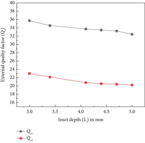
The extracted external quality factor (Qe) results are illustrated in Figure 18. As the inset depth (Li) increases from 3 to 5 mm, both Qe1 and Qe2 decrease. The parameter Li is optimized to achieve the required values of Qe1 and Qe2.
- 1.
Initially, determine the theoretical coupling parameters (Qe1(Qe2) and M1(M2) for the desired passbands from the low-pass prototype g-parameters using (1).
- 2.
Determine the dimensions of the SIW cavity using Equations (2) and (3).
- 3.
Consider the fundamental mode TE101 and the higher mode (TE102) for Passband I and the next two higher modes (TE201 and TE202) for Passband II.
- 4.
Introduce vias (V1, V2, and V3) and slot perturbations in the SIW cavity to shift the resonance frequencies of modes.
- 5.
Then, vary the diameter of via V1 to perturb fundamental mode TE101 towards TE102 to obtain M1 for Passband I.
- 6.
Next, vary the position of vias V2 and V3 and length of slots to perturb TE201 and TE202, respectively, to obtain M2 for Passband II.
- 7.
Finally, the inset depth (Li) and inset gap (Ig) of the feedline is varied to achieve the required Qe1 and Qe2 for both the passbands.
3. Fabrication and Measurement
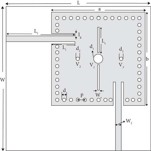
The final dimensions of the proposed dual-band filter shown in Figure 1 are L = 25 mm, W = 25 mm, a = 14.6 mm, d1 = 0.8 mm, d2 = 0.3 mm, d3 = 0.3 mm, LS = 4.45 mm, WS = 0.1 mm, Li = 4.1 mm, Ig = 0.3 mm, Wf = 1 mm, Lf = 12 mm, d = 0.6 mm, and p = 1.2 mm.
The proposed SIW cavity, fabricated on an RT/Duroid 5880 substrate, is measured using an Anritsu MS46524B vector network analyzer (VNA) to obtain the S-parameters. Figure 19 presents the simulated and measured results of the dual-band SIW filter with CFs at 16.2 GHz and 19.1 GHz. The simulated FBWs for the Passband I and Passband II are 1.74% and 3.14%, respectively, with ILs of 0.59 and 0.9 dB and reflection coefficients of −18 and −19.2 dB. The measured FBWs for the Passband I and Passband II are 1.71% and 3.09%, with IL values of 1.8 and 1.9 dB and reflection coefficients of −11 and −14.8 dB.
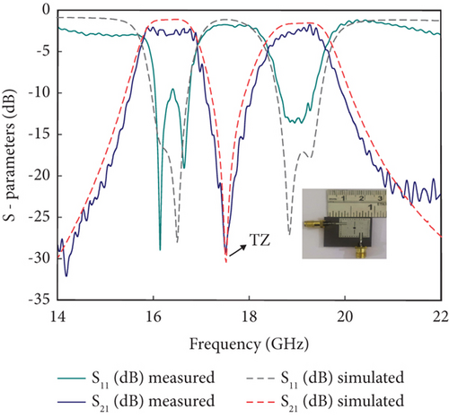
Table 1 compares different dual-band SIW BPFs with their CFs, IL, and size. The proposed design is in agreement with the size and IL.
| Ref. | CF (GHz) | IL(dB) | FBW (%) | Size () |
|---|---|---|---|---|
| [18] | 26.5/31.5 | 0.48/0.67 | 3.6/2 | 1.5∗2.2 |
| [19] | 2.51/5.30 | 1.41/1.88 | 6.8/5.8 | 0.23∗0.45 |
| [20] | 9.5/15.95 | 2.77/2.42 | 2.7/4.9 | 0.98∗0.98 |
| [21] | 6.22/8.24 | 0.86/1.32 | 7.7/3.9 | 0.89∗0.41 |
| [22] | 8/11.4 | 2.26/3.07 | 3.01/2.46 | 2.17∗2.17 |
| [23] | 9.8/13.5 | 1.8/1.5 | 11.8/9.8 | 1.22∗1.22 |
| [24] | 6.0/12.0 | 0.79/1.39 | 18.3/29.1 | 0.92∗0.53 |
| [25] | 18.8/19.4 | 0.68/0.61 | NA | 1.15∗1.15 |
| [26] | 46.7/60 | 2/2.8 | 11.7/6.8 | 1.8∗1.77 |
| [27] | 42.8/60.5 | 1.9/1.4 | 6.1/7.7 | 1.14∗1.64 |
| This work | 16.2/19.1 | 1.8/1.9 | 1.71/3.09 | 0.41∗0.41 |
4. Conclusion
This paper presents the design of a compact dual-band BPF using a multimode perturbation within a single SIW cavity resonator. The fundamental TE101 mode and the first higher order TE102 mode form the Passband I, with a CF of 16.2 GHz, an FBW of 1.71%, and an IL of 1.8 dB. The Passband II is formed by the higher order TE201 and TE202 modes, with a CF of 19.1 GHz, an FBW of 3.09%, and an IL of 1.9 dB. The proposed filter features a compact size, low IL, and independently controllable FBW.
Conflicts of Interest
The authors disclose that BITS Pilani, Hyderabad Campus, has provided funding and support related to this research. However, this does not affect the integrity or objectivity of the study.
Funding
BITS Pilani, Hyderabad Campus, supported this research. The authors acknowledge the financial and technical support provided.
Open Research
Data Availability Statement
The data that support the findings of this study are available from the corresponding author upon reasonable request.


